F.A. Shirland*, T.A. Griffin*, and G.H. Dierssen^
The Harshaw Chemical Company,Cleveland, Ohio Abstract
A new photovoltaic cell made from a film of CdS vacuum evap- orated onto a metal foil substrate is described. Such cells are being made in sizes up to 3 in. x 3 in., at conversion eff- iciencies of 2 to 3%* They can be laminated in plastic envel- opes to form arrays delivering 10 to l£ w/lb. It is estimated that these cells can be made very economically. Typical I-V characteristic, spectral response, and temperature performance curves are given. Data on the stability of these front wall CdS cells, including resistance to radiation damage, are also presented. Possibilities for larger area, lighter weight, higher efficiency cells of this design are discussed.
Introduction
Expanding requirements for space power emphasize the need for solar conversion devices with more watts per pound of system weight and more watts per dollar of cost. Major progress to- wards these objectives has been achieved with the CdS film cell.
This cell was first reduced to practice in the Laboratories of The Harshaw Chemical Company and was described at this meeting just two years ago.l
Presented at the ARS Space Power Systems Conference, Santa Monica, Calif., September 2^-28, 1962. This work has been
supported by the Air Force Research Division, Air Research and Development Command, U.S. Air Force under Contract AF 33(616)-
7528 with Donald C. Reynolds of the Aeronautical Research Lab- oratory and Joseph Wise of the Aeronautical Systems Division acting as Contract Monitors, and by the Lewis Research Center of NASA under Contract NAS 3-1850 with Andrew E. Potter acting as Contract Monitor.
-x-Research Section Head.
^Senior Research Physicist.
^Senior Research Chemist.
SHIRLAND, GRIFFIN, AND DIERSSEN
Those first CdS film cells were rear wall cells of the gen- eral construction shown in Fig, 1. Soft lime or pyrex glass, about O.OUO-in. thick was used as substrate. The glass was given a transparent conductive coating of Sn02« A layer of CdS, 0.002-in. to 0.005-in. thicks was vacuum evaporated onto the SnC>2 coating. A barrier layer was formed on the upper surface of the CdS film and contacted with a layer of conductive silver paint. The light reached the active "barrier" region by first passing through the glass and the GdS film itself — hence the
term "rear wall" cell.
The cells described here two years ago were as large as 1-1/2 x 3 in. in area and had conversion efficiencies of about 2%.
Smaller area cells with efficiencies as high as 3.5$ had been attained and since then 5% has been measured. It was evident at that time that such cells could be made more economically than the conventional smaller area higher efficiency single cry- stal solar cells. It was hoped that the weight of such cells could be drastically reduced to yield higher watts per pound of system weight.
Since most of the weight of this cell was in the substrate, considerable effort was expended in an attempt to develop thin- ner, lighter weight, transparent conductive substrates compat-
ible with vacuum evaporated CdS films. Very thin glasses, sheets of mica, plastic films, and various glass and quartz fabrics were tried with different methods of rendering these
substrates conductive. Mixed results were obtained, yet no one method seemed to offer a satisfactory combination of performance and practicality.
Front Wall Film Cell - Design
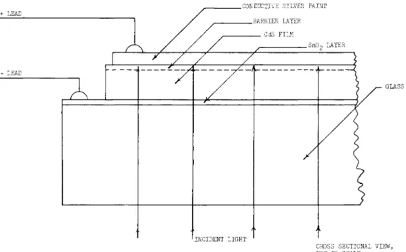
Hence, an alternate design, the "frontwall" CdS film cell, was developed which did not require a transparent substrate.
The construction is shown in Fig. 2, and is inherently simpler than that of the rear wall cell. The metal foil substrate acts as negative collector electrode. The light is incident direct- ly on the barrier surface. It is evident that this design makes possible truly thin photovoltaic cells, since very thin metal substrates can be readily obtained.
The present cell consists of a vacuum evaporated CdS film, 0.00l5-to 0.002-in. thick, on a metal foil substrate of about the same thickness. Molybdenum has been preferred as substrate material because its coefficient of thermal expansion matches that of CdS, but other metals including silver and gold have been used. The positive collector electrode is a fine silver screen that is held in contact to the barrier surface by means
336
of a laminated plastic layer.
The CdS front wall cell is now 2 to 3% efficient, is produced in areas up to 3-in. sq., and yields about 10 to l£ w/lb of array weight. These front wall cells show promise of still higher efficiencies, larger areas, and greater power outputs per unit of weight.
Front Wall Film Cell - Characteristics
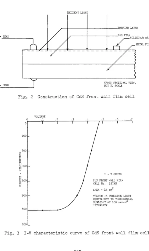
Figure 3 gives the I-V characteristic curve of a front wall CdS film cell. This cell was 2.9% efficient in simulated equivalent sunlight of lOOmw/cm^ intensity. As can be seen from the slope of the curve as it crosses the axes, there is room for improvement in reduction of series resistance and in- crease in shunt resistance.
The spectral response of the CdS front wall film cell is given in Fig. 1+, and is compared with the response of the same cell tested as a rear wall cell. The front wall cell response ex- tends into the ultraviolet, since the CdS itself is not filter- ing out these shorter wavelengths as it does in the case of the rear wall cell.
In spite of the broader response the front wall construction usually gives less output. The reasons for this are not en- tirely clear and are presently being studied.
The response curves of Fig. k were taken by conventional techniques using a standard monochromator, measuring the cell output at each wavelength and normalizing for constant light energy input. These data were from stabilized readings that were taken in each case after permitting the traps, which might have been filled during the previous reading, to empty. This slow trapping phenomenon was described in our earlier paper, and is an important feature of the operation of the CdS photo- voltaic cell.
A consequence of this feature is that the output of a CdS cell is greater when several suitable wavelengths of light are applied to the cell at the same time than the sum of the out- puts obtained from the same wavelengths applied separately.
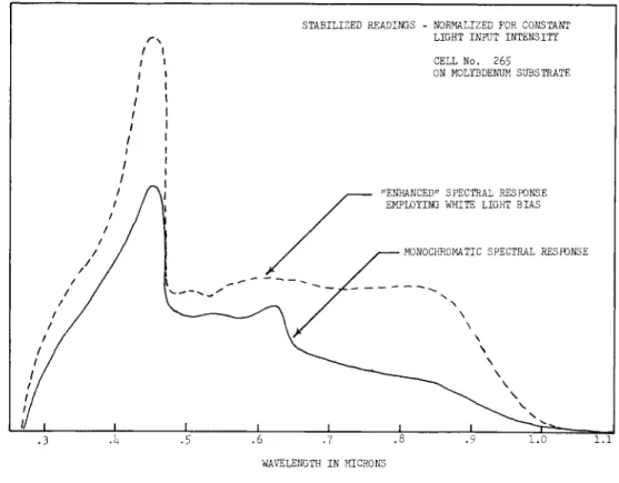
This ,renhancement is illustrated in Fig. 5. The solid curve represents the stabilized monochromatic response of a 1.0$
efficient front wall film cell. The dashed curve is the re- sponse obtained when a white light bias is applied, the photo- voltaic response from the white light bias being substracted in each case. This enhanced response is believed more representa- tive of the cell output when illuminated by a broad spectrum
SHIRLAND, GRIFFIN, AND DIERSSEN
light source, such as the sun.
A wide variety of enhancement patterns have been obtained, varying with the trace impurities in the CdS material. Con- siderable control of the density and energy level of trapping centers appears to be feasible. This may make possible CdS cells with spectral response curves specially tailored to specific incident light spectra.
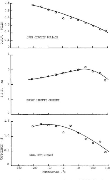
Accurate temperature performance data have been difficult to obtain for the CdS front wall film cell due to secondary ef- fects such as loss of electrical contacts and atmospheric de- gradation. Excluding such secondary effects, CdS single cry- stal cells, rear wall film cells on glass substrates, and front wall cells on molybdenum substrates all seem to have similar
temperature performance characteristics.
Figure 6 presents typical temperature performance data taken on a small area, 1.5% efficient, front wall cell between -100 and +l50°C. The open circuit voltage is seen to decrease near- ly linearly as temperature increases over this range. The short circuit current increases with increasing temperature, reaches a maximum at about 75°C, and then falls off fairly rapidly. There seems to be relatively little decrease in ef- ficiency up to about 50°C, followed by a rapid fall off at higher temperatures. This apparently results from the sharp break in the short circuit current curve, though the reasons for this are not understood.
Arrays of CdS Film Cells
The thinness, flexibility, light weight, and large area of the CdS front wall film cell make possible new designs for solar cell arrays in space applications. One design has been evolved that would permit the cells to be rolled up like a rug for launch and then unrolled in space. In this design an array is constructed by making a lay-up of cells and connecting them in a desired series-parallel hook-up using thin silver foil strips as leads and conductive epoxy cement for lead attachment.
The lay-up is then laminated between thin sheets of transparent plastic film. Mylar, polyethylene and other plastic films have been used successfully, but best results have been obtained with a Kel-F nylon composite film. The Kel-F envelope gives greater ruggedness to the array combined with some moisture protection.
The nylon forms a well adhering interphase at the cell surface.
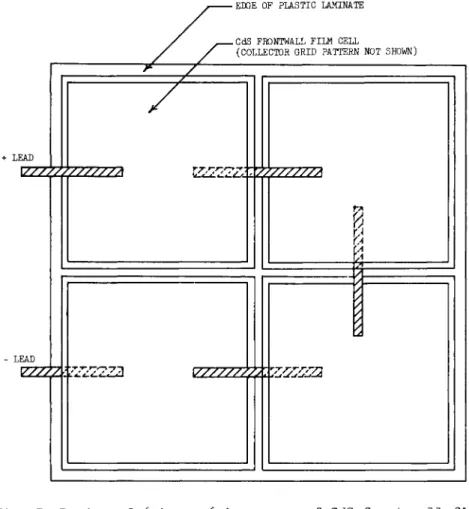
Figure 7 shows how four 3-in. x 3-in. CdS front wall film cells can be arranged in series to form a 6-in. x 6-in. array.
338
A number of arrays of this type, up to 12-in. x 12-in. in size, have been constructed for the Air Force and for NASA. The components comprising a 1-sq. ft. array that illustrates the present best state-of-the-art, are listed in Table 2. The weight of each component is given. The total weight of such an array could be as low as 73.6g or 1/6 lb.
At 2% conversion efficiency, the output of such an array in extraterrestrial sunlight would be 2.6 watt. This represents a power to weight ratio (for the array alone) of 16 w/lb. There are expectations of improving this ratio by further reducing the thickness of the substrates, CdS films and plastic foils used, and by increasing the efficiency of the cells. A two or three fold increase in the ratio is believed realizable in about the next year.
Stability of Arrays
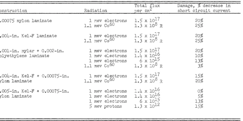
There have been indications that CdS film cells might possess appreciable resistance to radiation damage.-^ Such resistance might be expected because of the polycrystalline nature of the CdS film, the extreme thinness of the CdS barrier region, and because of the lower initial conversion efficiencies.^ A num- ber of accelerated radiation damage tests have been conducted on different CdS film cells at the U.S. Naval Research Labora- tory. 5+6
Table 2 lists the results of tests on individual cells ex- posed to radiation. Each line of the table represents a test
of a single cell. The cells were initially about 1% efficient.
A number of additional tests, where complicating secondary ef- fects, such as overheating, delamination of the plastic, or atmospheric degradation are believed to have occurred, were ex- cluded from this listing.
It appears that CdS film cell arrays can possess appreciable resistance to damage by radiation of the types normally associ- ated with the Van Allen belts. More data, particularly on higher efficiency cells, are needed.
CdS cells have been stable in dry air or in vacua, but have degraded severely in the presence of moisture. Single crystal CdS cells readily are protected from degradation due to mois- ture in the atmosphere by encapsulating them in thick layers of epoxy resin. CdS single crystal solar batteries with ef- ficiencies of 3 to %.h%> which were protected in this manner, have shown no measurable decrease in output after 3 years of ordinary room atmosphere storage. Rear wall CdS film cells
SHIRLAND, GRIFFIN, AND DIERSSEN
could be protected readily from atmospheric degradation by laminating a thin moisture impervious metallic foil against the barriers with insulating epoxy cement.
The CdS front wall construction is not protected so readily from moisture during atmosphere storage since the protective layer must be transparent. Kel-F appears to have the'least moisture permeability of any of the transparent plastic films
tested in our laboratories. Cells laminated in O.OO^-i^. Kel-F plastic envelopes and stored in normal room atmospheres3 with humidities in the 30 to 10% range, held their efficiency for about 100 days and then started to show appreciable degradation Thinner Kel-F and other plastic laminates did not hold up as long. Completely unprotected CdS film cells in ordinary atmos- phere storage degraded to almost no output within a week or two. Such degradation appears to be reversible and most cells so degraded can be restored to their original output by drying them. Fortunately, there is no moisture problem in the space environment and hence for these applications it is probably adequate to protect the cells until just prior to launching.
CdS front wall film cell arrays stored in inert gas atmos- pheres , dry atmospheres and in vacua have shown no degradation
during storage periods up to 200 days.
Other Considerations
The process for fabricating CdS evaporated film solar cells is essentially a simple one that should be amenable to auto- mation. Cleaning of substrates, evaporation of CdS films, barrier formation and electroding are operations that could be done on a continuous basis. There are no single crystal grow- ing steps involved. The raw material required is available commercially from several phosphor suppliers at moderate cost.
The process for laminating the cells into arrays is also simple involving no particularly difficult operations. While the lower efficiency CdS film cells will require a larger area array for a given power rating, the cell areas are so much larger that fewer cells need to be handled.
The present 3-in. x 3-in. film cell gives an active cell area of 50 to 55 cm^. Cells as large as 6-in. x 6-in. probably could be made now with essentially the same characteristics.
The major problems would be of a tooling nature. Cells as large as 12-in. x 12-in. in size are undoubtedly possible but would require more development work before they could be real- ized. There seems little to be gained in attempting to fabri- cate cells larger than this, and even the square foot size may
340
not be worth the additional effort.
It is difficult to estimate costs for a new product that still is undergoing extensive research and development. Pre- liminary estimates may be too optimistic since required in- creases in performance may be possible only by increasing material and processing costs. Using present design and pro- cessing as a guide, anticipated manufacturing costs for CdS front wall solar cells are in the range of $10 to $50 per watt.
Table 1 Components of 1 sq ft CdS Front Wall Film Cell Array
1 sheet 0.001-in. Kel-F + 0.00075-in. nylon laminate - 13-in.
x 13-in. 8.9 g 16 sheets 0.00l5-in. molybdenum metal foil - 3-in. x 9-in.
36.0 g lllU sq in. CdS evaporated film - 0.00l5-in. thick 16.8 g Silver foil leads and collector grids l.lj g 1 sheet 0.00l5-in. Kel-F - 13-in. x 13-in. 10.5 g
Total Weight 73.6 g
Table 2 Accelerated radiation damage tests on CdS front wall film cells
CO to
Construction
0.00075 nylon laminate
0.00U-in. Kel-F laminate
0.001-in. mylar + 0.002-in.
polyethylene laminate
0.00lt-in. Kel-F + 0.00075-in.
nylon laminate
0.005-in. Kel-F + 0.00075-in.
nylon laminate
Radiation
Total flux per cirr-9
Damage, % decrease in short circuit current 1 mev electrons
1.1 mev Co6 0 1 mev electrons 1.1 mev Co6 0
1 mev electrons 1 mev electrons 1 mev electrons 1.1 mev Co6 0
1 mev electrons 1.1 mev Co6 0
1 mev electrons 1 mev electrons 1 mev electrons 5 mev protons
1.5 x lO^7 1.3 x 10⁸ R 1.5 x 10^7 1.3 x 10° R
,5 x 1017 Л x lO1^ 6 x 10^5 ,3 x 108 R 1.5 x 10^7 1.3 x 10° R 1.1; x lO1^ l.U x lO1^ 6 x lO1^ 1.3 x 1 01 2
25$
13$
3$
15$
13$
15$
>
p
z
o
>
z
CO
References
Middleton, A . E . , Gorski, D.A., S h i r l a n d , F . A . , »Evapo-
r a t e d CdS f i l m p h o t o v o l t a i c c e l l s f o r s o l a r energy conversion,"
ARS P r e p r i n t 1291-60 (September 1962).
2
Shirland, F.A., Wolff, G.A., and Nixon, J.D., "Research on solar-electrical energy conversion employing photovoltaic pro- perties of semi-conducting cadmium sulfide,11 Aeronaut. Systems Div. Tech. Documentary Rept. 62-69 (January 1962).
3
Rappaport, P., Radio Corporation of America Laboratories (February 1962).
h
Smits, F.M., "Report on solar cell work at Bell Telephone Laboratories/ Solar Working Group Conference, 1APG, Radiation Damage to Semiconductors , Washington, D.C. (February 1962).
Brancato, E.L.,private communications, U.S. Naval Research Laboratory (February 1962).
6
Statler, R.L., private communications, U.S. Naval Research Laboratory (February 1962).
CONDUCTIVE SILVER PAINT BARRIER LAYER
CdS FILM
CO
INCIDENT LIGHT
GLASS
Co
>
z o o
>
z
co co
CROSS SECTIONAL VIEW, NOT TO SCALE
Fig. 1 Construction of CdS rear wall film cell
INCIDENT LIGHT
LEAD
A
"XZ7-
-BARRIER LAYER
COLLECTOR GRID METAL FOIL
CROSS SECTIONAL VIEW, NOT TO SCALE
Fig. 2 Construction of CdS front wall film cell
VOLTAGE 0 . 1
I - V CURVE CdS FRONT WALL FILM CELL No. 157AN AREA = U6 cnT
TESTED IN TUNGSTEN LIGHT EQUIVALENT TO TERRESTRIAL SUNLIGHT AT 100 mw/cni INTENSITY
700 L
Fig. 3 I-V characteristic curve of CdS front wall film cell
MONOCHROMATIC SPECTRAL RESPONSE CURVES STABILIZED READINGS - NORMALIZED FOR CONSTANT
LIGHT INPUT INTENSITY CELL No. 700 ON GLASS SUBSTRATE
CO 05
.FRONT WALL CdS FILM CELL
Co
>
Z o O
>
Z o
.6 .7
WAVELENGTHS IN MICRONS
9 1.0
Fig. 1; Spectral response of rear wall and front wall CdS film cells
CO
< 1
/
f 1 1 1 1
1 1
f
1
l Г\ 1 i / \
/ / i \ f / t 1
/ / ' /
/ / / / i ^^~ ' ^ ^^S"
/ / V
/ / ^ ^_^^
/ / / /
1 / 1 1
1 1 / if If
-j/_l 1 1 L
CELL No. 265
ON MOLYBDENUM SUBSTRATE
У "ENHANCED" SPECTRAL RESPONSE / EMPLOYING WHITE LIGHT BIAS
/ y MONOCHROMATIC SPECTRAL RESPONSE
* / / s
" — — - _^ /
S "S
( / N
\ / ^
\ X ^
\ Ч
V \
^ ^ ^ • « ^ N-—^__ \
'—\\ \ ч \ v . 4
^ ^ ^ N-
i i ' ^ ^ ^ - — 1
T3
o
CO -<
CO -i m
CO
>
П
O
.3 .5 1.0
WAVELENGTH IN MICRONS
Fig. 5 Spectral response of front wall CdS film cell illustrat- ing enhancement
SHIRLAND, GRIFFIN, AND DIERSSEN
0.6 0.5 o.U
§ 0.3 o > , 0.2
>
o 0.1 o 0
h
3k
l . S -
0.5
OPEN CIRCUIT VOLTAGE
SHORT CIRCUIT CURRENT
CELL EFFICIENCY
-150 -100 -50 0 TEMPERATURE -°C
50 100 150
Fig. 6 Effect of temperature on output of CdS front wall film cells
348
-EDGE OF PLASTIC LAMINATE
CdS FRONTWALL FILM CELL
(COLLECTOR GRID PATTERN NOT SHOW)
Fig. 7 Design of 6-in. x 6-in.
cells
array of CdS front wall film