RFID cards on biodegradable substrates – Realization aspects and future trends
Attila Géczy, Gergely Horváth, Levente Dudás László Gál, István Hajdu, Gábor Harsányi
Budapest University of Technology and Economics Dept. of Electronics Technology
gattila@ett.bme.hu
Abstract
The aim of the work was to investigate the technological aspects of pro- ducing ISO/IEC 14443 contactless RFID cards on biodegradable cellulose- acetate (CA) biopolymer-based Printed Circuit Boards (PCB), where the manufacturing steps and the actual parameters of the prepared cards were also investigated. The general motivation behind the work was to find an ap- plication for such biodegradable substrates, meanwhile reducing the amount of generated E-Waste. The technology of the coil wiring is based on PCB manufacturing steps to obtain low cost producibility. The assembly of the board with standard Mifare1K chip is based on Surface Mount (SM) elec- tronics assembling technology. The preliminary results show accurate and functional example of a ISO 14443 standard 13,56 MHz RFID reference card.
Keywords:RFID, Biodegradable, Contactless Card, Cellulose Acetate
1. Introduction
Electronic waste is a critical aspect of global electronics production, while the gen- erated amounts are increasing year by year. [1] Novel approaches and materials are required to reduce the produtcion of harmful electronic waste. Recycling and waste processing is a complex task, while most of the electronic materials are essen- tially non-degradable. Printed Circuit Boards (PCB) are one of the most harmful components of the generated e-waste, so the need to find biodegradable substitutes for the basic PCB substances is an important part of the question. Only limited
Eszterhazy Karoly University of Applied Sciences and Bay Zoltán Nonprofit Ltd. for Applied Research Eger, Hungary, November 5–7, 2014. pp. 35–42
doi: 10.17048/FutureRFID.1.2014.35
35
experience is available about the applicability of biodegradable substances in elec- tronics, and despite the advantageous properties of the materials, these solutions are rarely presented in commercial electronics. The specific material parameters of the biodegradable materials also raise new questions - it is a challenge to make the material compatible with the traditional assembling technologies of electronics.
Our previous investigations show [2-4] limiting factors of solder joint production (lower melting point and glass transition temperature of substrate), and PCB fab- rication - however initial results are promising. The paper presents a possible new application form of the biodegradable substrates, where a contactless RFID card was produced within the dimensional confines of the ISO/IEC 14443 standard.
2. Motivation
Bioplastics are a special field of polymers; their popularity has started in the 1950’s.
In the late years of the 20th century new applications come into focus and elec- tronics also emerged as a possible field of use for bioplastics. These substrates [5,6] can be divided to the following plastic classifications: "compostable and bio- logically degradable polymers (DIN 12432 [7])" and "plastics based on renewable resources".
Bioplastics also could be divided into "biodegradable / compostable but not bio-based", "biodegradable / compostable and bio-based" and "non-biodegradable but bio-based" types. Previously a patent was introduced to present a completely degradable RFID tag [8], also even more advanced electronic designs were composed from degradable polymers [2,3,4,9]. Recently the capability of different biodegrad- able materials in electronics were directly investigated [10]. Also inkjet and gravure printing technology was introduced for electronic conductors application on specific biodegradable materials [11].
For our experiments a promising research path was chosen for biodegradable- based contactless RFID card production - the substrate technology is totally com- patible with standard PCB production and widely used reflow asseembling - making the whole process affordable. The next chapters present the experimental setup and the pilot results of our experiments.
3. Experimental
In order to produce a pilot series of RFID cards, we chose the widely used 13.56 MHz range and we have investigated standard, commercial ISO 14443 cards as a starting, reference point, with the widely known Mifare1K integrated circuits.
Figure 1 shows the X-Ray analysis of a commercial RFID card (TWC-401-100 Mifare S50), where the antenna and the chip is clearly visible. This commercial sample served as a starting point for further design choices. For evaluation of the commercial and the proposed biodegradable based pilot cards, a SLO40 USB 13.56 MHz card reader was chosen to enable functional testing.
Figure 1: Standard, commercial ISO 14443 RIFD card (segmented X-Ray analysis)
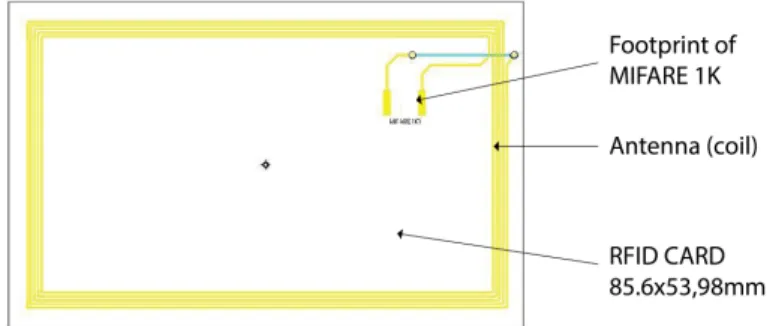
According to the standard geometry and the approximating coil parameters of the required 13.56 MHz range a pilot card design was produced in a PCB designer tool (Mentor Graphics PADS). The design slightly differs from the commercial card (which has a winded/embedded coil, rather than a PCB coil track). Figure 2 shows the layout of the proposed pilot card, where the geometry data is prepared for computer aided manufacturing of standard PCBs.
Figure 2: Pilot RFID card in PCB designer tool
To produce PCBs a selected biodegradable polymer material was applied for substrate board production: cellulose-acetate (CA). CA has favourable parameters for application in electronics, and can be compatible with fast Vapour Phase Solder- ing technology. The density of the material is 1.29 g/cm3, the melting temperature is around 185 degrees C (it is a must, to avoid common lead-free solders, such as SAC305), and the glass transition temperature is around 105 degrees C. CA was available in pellet form, which is the starting form to mould the actual substrate in an injection moulding machine. The parameters of the produced boards (surface roughness, dimensions, etc) are mainly depending by the machine setup. After the moulding, copper foil is laminated onto the base boards with a HML MP 20- VK type laminator. During lamination the maximal temperature is 165 degrees C
which is optimal from the aspect of CA material. PCB tracks are produced on the laminated structure with subtractive methodology. The CA boards were prepared for reflow soldering. The steps of this method are the following: stencil printing of the solder material in paste for, automated or manual component placement and finally heat transfer. A special paste was selected to match the low temperature pa- rameters of the material (NC-SMQ81; composition: 58Bi/42Sn) with the melting point of 138 degrees C. For heat transfer an experimental vapour phase soldering station (presented in [4]) was used with Galden HT170 fluid. The station uses Lab- VIEW SW+HW setup to control the sample holder inside the oven for precise heat transfer. Sample cards were also produced from standard FR4 PCB material based on the PCB design data to enable comparison with a totally standard electronic panel.
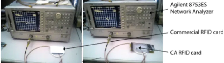
For evaluating the produced cards the two following methods were applied. The reading distance of the card and the card reader were obtained with a Balluff BTL5 micropulse transducer, where the card was fixed to a sample holder. The reader was positioned paralell with the card, and then moved on a normal axis to the surface of the card with the precision of 0.01 mm. The reader indicates the proximity with a signal sound. The other method involved an Agilent 8753ES network analyzer (showed in Figure 3) to reveal the resonance frequencies of the cards in comparison to the commercial one. Also a Tektronix DPO 7254 Oscilloscope was used for analyzing the signal of the reader from the side of the card.
Figure 3: Agilent 8753ES Network Analyzer setup
4. Results of card production
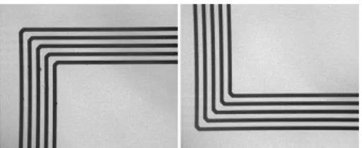
The production of the CA PCBs was succesful, however some minor problems were revealed during optical microscopic analysis of the first pilot cards. Figure 4 (left) highlights a problem, where results of the masking/etching process during PCB fabrication caused some issues along the tracks, where several shorts had to be manually removed from between them. Also some spots were observable on the surface which was due to the etchants used in the process. Figure 4 (right) shows special delaminations of the tracks in the upper right corner. This effect is due to the imprecisions of the board moulding. If gases are trapped in the moulded board, the voids inside the substrate will be relased during the PCB fabrication
steps. This can negatively affect the copper adhesion on the substrate, even causing delamination and tear damage.
Figure 4: Initial problems of PCB production. Left - removed shorts from between tracks. Right - delaminated tracks in the upper right corner, due to trapped gases in the base substrate (assembled
picture of an optical microscope)
Figure 5 shows the X-Ray analysis of a CA card, where the track shapes on the PCB are normal, without any shorts or deformations.
Figure 5: X-Ray analysis of given PCB tracks
A specific card (without the presented problems) was chosen for further inves- tigations and pilot assembling. Figure 6 presents the manual pick and place step of the Mifare1K chip. The solder paste was previously deposited on the contact pads of the substrate. Note that the card was not cut out of the PCB panel at this step of the production to enable easier handling.
5. Results of measurements
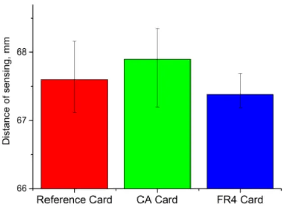
To evaluate the reading distance of our pilot card, the distances were compared with the reference card and the FR4 sample. Figure 7 shows the results of the distance measurements.
It is apparent from the results, that the distances are really close to each other between 67 and 68 mm, which practically means the reading distances are the same from the aspect of ergonomic usage. The slight advantage of the CA card is minimal and practically negligible (around 0.2 mm), and can be due to small measuring imprecisions. The next figure (Fig. 8) shows a case, where the CA RFID card was moved to contact proximity of the reader.
Figure 6: Pick and place assembly of the RFID card
Figure 7: Results of reading distance measurements – CA RFID cards give promising results regarding usability
The figure (obtained from the oscilloscope) presents that with the decreasing distance, the signal amplitude increases and reaches its maximal value (4 V) in the end, when the card contacts the reader. The signal waveform is practically the pulse train of query, coming from the reader.
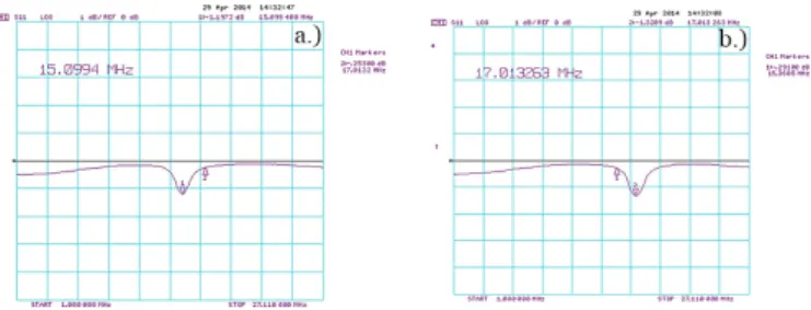
The reference and the CA card was compared from the aspect of resonance frequency, in order to evaluate the antennas. The results show (Fig. 9), that both resonance values are far from the precise 13.56 MHz, however from the aspect of usability, both approximations are turning out to be sufficient and satisfactory. The difference is due to the antenna shape, which was designed with PCB production and basic PCB track design rules in mind (without arcs in the tracks).
6. Conclusion
Our aim was to make an RFID card from biodegradable substrate, where the tracks of the antenna and the footprint of the IC is produced with standard PCB tech-
Figure 8: Oscilloscope analysis of the radio signal - 4 V is obtained at contact distance
Figure 9: Resonance frequencies of reference card (a.) and CA card (b.); Difference is due to minor changes in antenna geometry
nology, and the Mifare1K integrated circuit is soldered with standard reflow steps.
The presented results show promising paths of future experiments - the compatibil- ity with standard PCB manufacturing and reflow assembling makes our approach affordable and practical. Also the pilot card showed satisfactory results from the aspect of practical utilization as well. Future plans involve further optimization of the PCB track deposition on degradable substrate; also several different shaped and sized RFID tags are under test with the same production and assembling methodology. Cover layer lamination for the boards is also in our focus.
Acknowledgements. This work is connected to the scientific program of the
"Development of quality-oriented and harmonized R+D+I strategy and functional model at BME" project. This project is supported by the New Hungary Develop- ment Plan (Project ID: TÁMOP-4.2.1/B-09/1/KMR-2010-0002).
References
[1] Hogue, C. Growing Piles of Toxic Trash, Chemical and Engineering News ISSN 0009-2347, 88(9) (2010)
[2] Geczy, A. Lener, V. Hajdu, I. Illyefalvi-Vitez, Zs.Low temperature soldering on biopolymer (PLA) Printed Wiring Board substrateIEEE ISSE, (2010), 57-62.
[3] Geczy, A. Kovacs, M. Hajdu I. Conductive layer deposition and peel tests on biodegradable printed circuit boards,IEEE SIITME (2012) 139-142.
[4] Geczy, A. Garami, T. Kovacs, B. Nagy, D. Gál, L. Ruszinkó, M. Hajdu, I.
Soldering Tests with Biodegradable Printed Circuit Boards,IEEE SIITME (2013) 39-42.
[5] Kaeb, H.Bioplastics Bioplastics: Technology, Markets, Policies,4th European Bio- plastics Conference Berlin (2009)
[6] Bioplastics - Frequently Asked Questions (FAQs),www.european-bioplastics.org (ac- cessed at 2011. 04. 04.)
[7] DIN EN 12432 - Proof of compostability of plastic products
[8] Dani, B. Ivan, R, Robert, B. Boris, M.Biodegradable radio frequency identifi- cation cards,Patent no. 7492326
[9] Hadlington, S.Biodegradable electronics dissolve after useRoyal Society of Chem- istry http://www.rsc.org, (accessed at 2011 04. 04.),
[10] Schramm, R. Reinhardt, A. Franke, J.Capability of biopolymers in electronics manufacturingIEEE ISSE, (2012), 345 – 349.
[11] Vasquez Quintero, A. Frolet, N. Marki, D. Marette, A. Mattana, G.
Briand, D. de Rooij, N.F.Printing and encapsulation of electrical conductors on polylactic acid (PLA) for sensing applicationsIEEE 27th Internation Conference on Micro Electro Mechanical Systems (MEMS), (2014), 532 – 535.