Electrochemical Migration of SAC305 Solders and Tin Surface Finish in NaCl Environment
Sándor Ádám, Bálint Medgyes, Dániel Rigler, Bence Szabó and László Gál
Budapest University of Technology and Economics Budapest, Hungary
medgyes@ett.bme.hu
Abstract— The impact of chloride ion contamination on electrochemical migration (ECM) of SAC305 lead-free solder alloys, and galvanic tin surface finish was studied using water drop tests and by using an in-situ electrical and optical measuring set up as well.
Tests were performed with the use of 3.5 wt% NaCl solution. The “A” type SAC305 alloy had a rosin&acid/flux paste ratio of 12.5 wt%, however by the “B” type SAC305 alloy it was only 9.3 wt%. According to the mean-time-to-failure (MTTF) data it was shown that “A”
and “B” type solder alloys have approximately the same ECM susceptibility, but in the case of tin surface finish failures happened typically after shorter period of time.
Keywords— electrochemical migration; water drop test; lead-free solder alloys; SAC305; NaCl I. INTRODUCTION
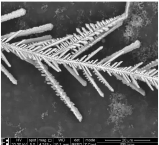
ECM is a failure process which may causes failures on adjacent metallization structures and poses huge reliability risk in operating electronics [1]. ECM occurs on dielectric-conductor-dielectric structures when certain climatic conditions (for example high humidity and temperature) are existed and the structure is under voltage. The phenomenon begins with oxidation at the anode, which resulted in metal ions. Due to the formed electric filed metal ions migrate from the anodic site to the cathodic site, where they are able to reduce and form the so called dendrites (metal filaments) (See Fig 1.) [2]. These dendrites can causes electrically shorts and can also causes an irreversible value decrease of the surface insulation resistance. Smaller distances between loaded traces/pads on the printed circuit board (PCB) assembly could increase the probability of ECM.
The
ECM behaviour is mainly checked by water drop (WD) tests or environmental tests in climatic chambers or thin by electrolyte layer (TEL) test as commercial investigation techniques [3]. Other techniques such as voltammetry tests are based on analytical techniques.Lead-free solder alloys are composed of metals such as tin, silver and copper. It was confirmed that these metals have significant capability for ECM failures [2]. Other parts of the solder paste such as activators in the flux could also modify the ECM behavior. Investigations of no-clean solder flux residues showed that using weak organic acid (WOA) activators with higher deliquescence point are better from the ECM point of view [4].
Contaminations also have great effect on the ECM phenomenon. Applied technological processes of electronics and normal environmental usage could result in the presence of different type of contaminator ions. Chloride ions could come from the air as evaporated sea-water, or from human perspiration in case of technological processes with human involvement.
The migration of SAC305 lead-free solder alloys with different rosin&acid/flux paste ratio in chloride environment was not yet investigated, however it was proven that flux residues have considerable effect on electrochemical migration [5].
Fig. 1. Dendrite on a PCB.
II. EXPERIMENTAL
Test boards applied in this work were made by fiberglass-epoxy resin (FR4) substrate with pure copper layer was covered by two types of SAC 305 lead-free solder alloys using stainless steel stencil printing and reflow soldering techniques or with galvanic tin surface finish. The “A” type SAC305 alloy had a rosin&acid/flux paste ratio of 12.5 wt%, however by the “B” type SAC305 alloy it was only 9.3 wt%.
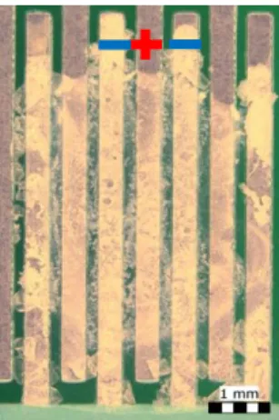
The gap size and the distance between the conductor pads on the test board was 0.3 mm in both cases, while the gap size was 0.3 mm. Fig. 2 shows the used reflow temperature profile for lead-free solder alloys in agreement with supplier’s recommendation (See Fig. 2).
Fig. 2. Reflow temperature profile for the test lead-free solder alloys.
With the test set up (See Fig. 3.) real-time voltage data was recorded while in-situ optical inspection of ECM formation was performed as well. Based on the electrical data (voltage change), the ECM processes were followed, and MTTF was calculated as well.
Fig. 3. Schematic of the test set up for ECM investigation.
The electrolyte used for the water drop test was a NaCl solution with a weight percentage of 3.5. It was created by high purity water (2 µS/cm) and from analytical grade components. Before each investigation, the surface of the PCB was rinsed with high purity water three times, and cleaned with ethanol as well. In each experiment a droplet of 10 µl was placed between the electrodes and 3 VDC test voltage was loaded.
The time of the failure determination was based on the first voltage change using the voltage diagrams. According to this principle criterion of the failure was the first significant voltage jump (See Fig. 4.). ECM measurements were repeated ten times on each type of solder alloy, surface finish to get adequate repeatability. Based on the voltage diagrams MTTF was calculated in case of each solder alloy and surface finish.
0 50 100 150 200 250 300
0 200 400 600
Temp er at u re (° C)
Time (sec)
Reflow soldering profile
Fig. 4. Time-to-failure determination by the first significant voltage jump.
After ECM tests optical microscopy (OM), Scanning Electron microscopy and Energy dispersive X-ray Spectroscopy (SEM- EDS) methods were also applied to analyze the chemical composition of dendrites and residues on the boards.
III. RESULTS AND DISCUSSION A. ECM results of “A” type SAC305 solder alloy in 3,5 wt% NaCl
Typically, right after the 3 VDC test voltage was loaded, 1500 mV value level was perceptible. The droplet was stretched, and H2 gas evolution was visible at the cathode. After a short period of time white colored precipitate appeared, nearby cathode side.
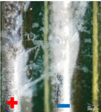
Outgassing and residue formation stopped after 2 minutes. Gray colored dendrites were grown from the cathode towards the anode (See Fig. 5.). In this case the MTTF value was 160 sec. Right after the measurement a typical test sample can be seen on Fig. 6.
From the VDC test voltage was loaded, until the failure processes occurred and increased the voltage level with 300 mV.
Fig. 5. Gray colored dendrites on the PCB in case of “A” type solder alloy.
Fig. 6. White residue formation was observable in case of “A” type solder alloy.
It was expected that the SEM-EDX results confirmed; the main element of the dendrites is tin, and precipitates primarily consist Sn and oxide (See Fig. 7.). Carbon, sodium, and chloride can be originated from the PCB material or from the NaCl electrolyte.
Fig. 7. SEM-EDX analysis in case of “A” type solder alloy.
B. ECM results of “B” type SAC305 solder alloy in 3,5 wt% NaCl
In case of “B” type solder alloys, after the 3 VDC test voltage was switched on, an initial voltage of 1500 mV was measured.
The droplet started to stretch, and H2 outgassing was observable at the cathode. After a half minute white residue appeared, near the cathode. Bigger amount of white residue was produced than in case of “A” type solder alloy (See Fig. 8). Outgassing and residue formation stopped after 2 minutes. Gray, metallic colored dendrites were grown from the cathode to the anode (See Fig. 9.), with different morphology than in case of “A” type solder alloy. Voltage increased with about 150 mV until the failure occurred.
Failures typically happened after 178 sec.
Fig. 8. Bigger amount of white precipitates was formed in investigations with “B” type solder alloy, than in case of “A” type solder alloy.
Fig. 9. Gray, metallic colored dendrites shown up in case of “B” type solder alloy.
SEM-EDX results showed that dendrites are mainly composed by tin (See Fig. 10.), and in the residue tin and oxide are dominant (See Fig. 11.).
Fig. 10. SEM-EDX analysis in case of a dendrite by “B” type solder alloy.
Fig. 11. SEM-EDX analysis in case of residue by “B” type solder alloy.
C. ECM results of galvanic tin surface finish in 3,5 wt% NaCl
WD test results with galvanic tin surface finish showed, that after the 3 VDC test voltage was loaded, voltage level at the resistor increased up to 1800 mV. After the stretching of the droplet the outgassing process was similar to the solder alloys. The color of the residue was white, but in this case bridging over the insulator layer was more typical (See Fig. 12.). Voltage at the resistor was not changed until the failure eventuated. MTTF was 99 sec. Gray, metallic colored dendrites were grown from the cathode to the anode, with similar morphology as in the case of “B” type solder alloy (Fig. 13.).
Fig. 12. White residue with bridging over the insulator layer was observed in case of galvanic tin surface finish.
Fig. 13. Gray, metallic colored dendrites in case of galvanic tin surface finish with similar morphology as in case of “B” type solder alloy.
Fig. 14. SEM-EDS analysis in case of galvanic tin surface finish.
According to the results of SEM-EDX analysis, similar to the other cases dendrites mainly contain tin, and the residue consists of tin and oxide (See Fig. 14.). In the residue Si, and Mg were also detectable, presumably these elements were originated from the PCB material.
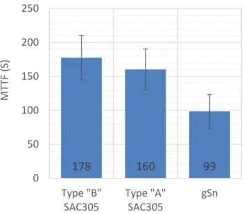
D. Comparison of solder alloys, surface finish from the aspect of MTTF
According to the MTTF data (See Fig. 15.) it was confirmed, that “A” and “B” type solder alloys with different rosin&acid/flux paste ratio have closely the same migration susceptibility with 160 and 178 sec. On the other hand, in case of galvanic tin surface finish, failures happened after a shorter period of time, the ECM mechanism was faster, MTTF was 99 sec.
Fig. 15. MTTF values between SAC305 solder alloys and galvanic tin surface finish (with 1σ deviation), in case of WD tests with 3,5 wt% NaCl solution.
Two-sample t-tests were also made in each pair. It was proven that on 95% significance level, the MTTF values by “A”, “B”
type solder alloys are the same, however t-tests also confirmed that MTTF value of gSn is different from the MTTF values of solder alloys on 95% significance level.
IV. CONLCLUSIONS
The impact of chloride ion contamination on ECM of lead-free solder alloys (with different rosin&acid/flux paste ratio) and galvanic tin surface finish was studied using water drop tests and by using an in-situ electrical and optical measuring set up as well.
Based on the MTTF results no significant difference was demonstrated between the “A” and “B” type lead-free solder alloys. In case of galvanic tin surface finish the migration susceptibility was higher than by the solder alloys.
SEM-EDX analysis results revealed in all three cases, that dendrites are mainly composed by tin, while the residues mostly contain tin and oxide.
ACKNOWLEDGMENT
Bálint Medgyes would like to thank the support for the National Research, Development and Innovation Office NKFIH, PD 120898. Bence Szabó would like to thank to the Pro Progressio Foundation (Hungary) for the financial support.
REFERENCES
[1] D. Minzari, F. B. Grumsen, M. S. Jellesen, P. Møller, R. Ambat, "Electrochemical migration of tin in electronics and microstructure of the dendrites", Corrosion Science, Vol. 53, 2011, pp. 1659–1669.
[2] B. Medgyes, B. Illés, G. Harsányi, "Electrochemical migration behaviour of Cu, Sn, Ag and Sn63/Pb37", Journal of Materials Science: Materials in Electronics, Vol. 23, 2012, pp. 551.
[3] X. Zhong, S. Yu, L. Chen, J. Hu, Z. Zhang, "Test methods for electrochemical migration: a review", Journal of Materials Science: Materials in Electronics, Vol. 28, pp. 2279-2289, 2017.
[4] V. Verdingovas, M. S. Jellesen, R Ambat, "Solder flux residues and humidity-related failures in electronics: relative effects of weak organic acids used in no-clean flux systems", Journal of Electronic Materials, Vol. 44, No. 4, 2015, pp. 1116-1127.
[5] V. Verdingovas, M. S. Jellesen, R Ambat, "Impact of NaCl Contamination and Climatic Conditions on the Reliability of Printed Circuit Board Assemblies", IEEE Transactions on Device and Materials Reliability, Vol. 14, No. 1, pp. 42-51, 2014..
.
178 160 99
0 50 100 150 200 250
Type "B"
SAC305
Type "A"
SAC305
gSn
MTTF (S)