Wetting of different lead free solder alloys during vapour phase soldering
Mohamed Amine Alaya, László Gál, Tamás Hurtony, Bálint Medgyes, Dániel Straubinger, Al-Maaiteh Tareq I, Balázs Illés, Attila Géczy
Department of Electronics Technology,
Budapest University of Technology and Economics, Budapest, Hungary
Abstract: In this paper the wetting properties of lead free solder alloys were investigated on different printed circuit boards (PCB) during Vapour Phase Soldering (VPS), which is an alternative reflow method with non-conventional heat-transfer mechanism. Our motivation was to investigate the phenomenon on PCBs with different thermal capacities, with different heating power and with different solder alloys. The aim of the research is to clear the relations between the thermal capacities of the) PCBs and the spreading of the solder on it, and to investigate the effect of the change of heating power on the solder spreading during VPS. In addition, the impact of the VPS on different solder alloys and the performance of the VPS machine in the wake of the contact angle quality was investigated. Findings show that the thickness of the PCB is not affecting significantly the spread and the wetting. The composition of the alloy, the paste, and the heating power points to observable differences in the final results.
1.INTRODUCTION
The vapour phase soldering (VPS) is a method of reflow soldering, using a system which applies hot vapour on the print circuit board (PCB), where the solder paste [1] and the components are already positioned. The vapour is used to heat the paste and the whole assembly [1,2,3], also the vapour medium itself is created by boiling the Galden fluid [4]. The VPS technology is recommended for many different electronics assembly applications because it provides unique advantages such good quality joints between the electronic components and the board, regular and fast heating of the components [1], minimalizing the voids inside the solder [5,6,], and safety from the aspect of inert heat transfer material [7]. The working method of the VPS starts with applying heating power on the bottom of the oven where the Galden is reserved. At the temperature of boiling, the liquid will change its phase
to hot vapour, and it is distributed inside the oven. In this paper, we investigate the efficiency of the reflow process of the VPS by applying the wetting test on solder alloy samples in a heat-level (HL) type VPS oven. In a HL-VPS oven the vapour is generated onto the surface of the board from the bottom (and not the PCB is immersed into the vapour). The experimental study of the spreading and contact angle, helps to improve the knowledge on the field [8,9,10,11].
Wettability investigations generally cover the contact angle measurements, when the solder paste interact with the PCB contact surface. Such wettability studies usually involve the measurement of contact angles as the primary data, which indicates the degree of wetting when a solid and liquid interact. Low contact angles (<<90°) point to high wettability, whilet large contact angles (>>90°) point to low wettability [12]. Angles can be reduced below 20° using the nitrogen in conventional convection-based reflow processes. [13] This paper focuses more on the impact of the condensation type heating on the spreading of solder in the following cases:
• The thickness of the PCB (thermal capacitance) is varied;
• The heating power of the machine is varied (variation of the temperature change speed and the vapour distribution), allowing different solder profiles [14];
• Different types of solder material are used;
• The quantity of the paste is increased.
2.EXPERIMENTAL
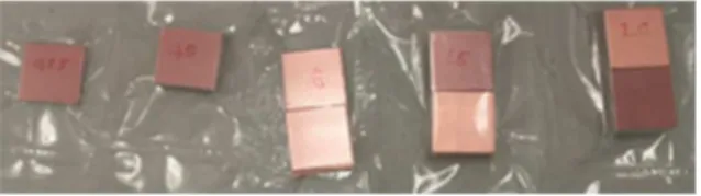
The reflow soldering had been performed with a a commertially avaible Asscon Quicky 450 vapour phase soldering system with Galden LS230 at Budapest University of Economics and Technology, Department of Electronics Technology [15]. Glass fibre reinforced FR4 epoxy resin boards were used with a copper foil on one side. The thickness of the boards ranged along the following values: 0.25, 0.5, 1, 1.5 and 2 mm (see Fig 1.).
Fig. 1. Different PCB samples from 0.25 to 2 mm thickness
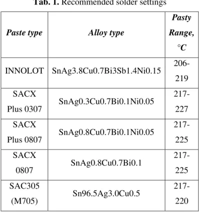
For the investigations, the following solder paste materials were used: INNOLOT, SACX Plus 0307, SACX Plus 0807, SACX 0807 and SAC305 (see Tab 1). The data was gathered from [16] and relevant paste datasheets.
Tab. 1. Recommended solder settings
Paste type Alloy type
Pasty Range,
°C
INNOLOT SnAg3.8Cu0.7Bi3Sb1.4Ni0.15 206- 219 SACX
Plus 0307 SnAg0.3Cu0.7Bi0.1Ni0.05 217- 227 SACX
Plus 0807 SnAg0.8Cu0.7Bi0.1Ni0.05 217- 225 SACX
0807 SnAg0.8Cu0.7Bi0.1 217-
225 SAC305
(M705) Sn96.5Ag3.0Cu0.5 217-
220 2.1. Measurement of the solder spreading on the surface of the board
The copper-clad FR4 boards were prepared according to the following method. To avoid the oxidation of the upper copper layer of the PCB, we followed the cleaning steps:
• Wet polishing;
• Final finish acid cleaning (MacDermid, 75039);
• Bleaching;
• Drying;
• Vacuum packaging prior to testing.
Two different stencil aperture setups were used to print the solder paste on the board, a set of four 2.3 mm round apertures was used as a general solution, the thickness of the stencil was 0.23 mm. Later 0.17 mm thickness was also introduced to reduce the amount of solder paste. In each experiment three PCBs were used with the aforementioned four paste deposits distributed on each PCB: for every experiment, we received data of 12 samples (see Fig 2.). It is important to mention that the time of the
PCB preparation should be short to avert the changing of the results characteristics due to the oxidation of the copper.
Fig. 2. PCB sample before the soldering
The PCBs must installed in the VPS oven in a way that the same temperature and same density of vapour is present, to ensure consistency on all the samples. All the samples were soldered with the same settings. The heating power was set to 60%, vapour temperature for process break was set to 180 °C and the heat delay to 10 s.
The measurement device used for the investigation of the samples is an OLYMPUS SZX9 stereomicroscope with a trinocular observation tube (SZX-TR30) for taking photomicrographs. A CanonEOS 1100D (12.2 Mpixels) was positioned directly over the system mount of the straight phototube.
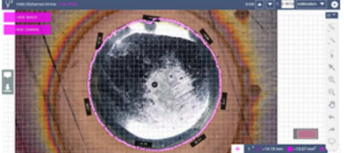
The software application used to measure the surface spread of the solder and its perimeter was SketchAndCalc (see Fig 3.); which is an irregular area calculator where it is possible to measure any shape with setting its scale without coding proprietary geometry calculators [17].
Fig. 2. SketchAndCalc software for area measurement
In the first experiment, the spreading test was applied on different PCB specimens (Fig 1.) with different thicknesses and same solder material (SAC305).
The heating power then was varied between 40-60-80-100%. The PCB thickness used in this experiment is 1.5 mm, due to its standard value in the industry; the used solder is SAC305.
Then the material (alloy) sweep followed this part of the experimental according to Table 1.
The thickness variation of the stencil (volume change of printed solder) concluded this part of the experimental on two different PCB thickness.
2.2. Cross section investigation to investigate the contact angle between the solder and the PCB The cross-section preparation is a delicate process and before performing sample cutting, there is a need to clean the samples. After soldering, the flux residue will cover some part of the sample. To remove it totally, the PCB was placed into the cleaning solution Shesto UTFLU01 [18] then it was followed by a cleaning with the isopropanol 2-propanol (CH3CH(OH)CH3) [19] for 1 min.
The next step is to embed the samples into two component acrylic resin and apply 2 Bar of pressure for 25 minutes.
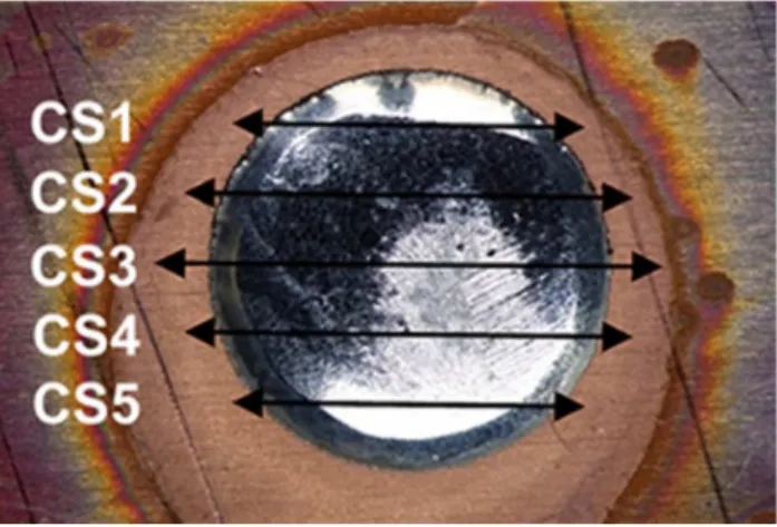
The samples had been cross-sectioned along five five cross-sectioning planes (see Fig. 4.); in each cross-sectioning plane we are able to measure the contact angle between the surface of the PCB and the solder material with microscope.
For the measurement of the contact angle an OLYMPUS BX51 materialographic upright microscope was applied. The camera system used is microscope digital camera OLYMPUS DP72, which is mounted on a camera adapter. Figure 4. shows the proposed cross-section cuts for evaluating the results.
Fig. 4. Cross section cuts on the sample
3.RESULTS
The experiment results are presented in the following subsections.
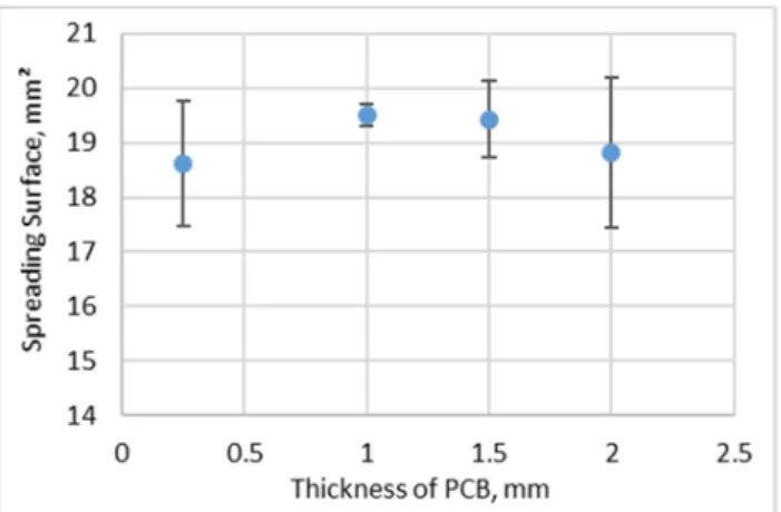
3.1 Result of spreading tests as a function of the thermal capacitance
The measurements have a similar average area spreading for all the PCB specimens. The minor deviation of measured values are shown in Fig. 5. It is clearly observable, that the final results are varying around 19 mm2; the averaged result for all the PCB specimens is ~19 mm² ± 0.5mm².
Fig. 5. The effect of the PCB thickness on the spreading of the solder
The measurements in Fig 5. show that the test is not affected by the thickness of the PCB specimen–
with the variation (increase) of the thickness, and the increase of the thermal masses of the boards, there is no observable difference on the wetting. This proves that the VPS oven is able to perform similarly with the increased thermal capacity of the substrates.
The deviation shown in Fig 5 may come from the fact that the surface of the copper clad laminate might show differences in roughness (as Figure 6 shows, the thickness variation of the copper clad might affect surface relations). Another possibility might be that the assemblies (board+paste) spent considerable time in ambient laboratory environment while waiting for the next VPS cycle, despite the fact, that the preparations were performed carefully, so that the samples do not spend more time waiting for the oven cycle than 30 minutes – this might also affect the wetting.
Fig. 6. The difference of the copper clad thickness
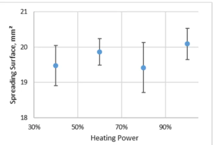
3.2 Result of spreading with varied heating power
The heating power does not have a significant role in the dynamics of the spreading (see Fig 7.).
Fig. 7. The effect of the heating power on the spreading of the solder
We can observe that there is no significant change in the spreading of the solder whenever the heating power is changed, but overall a slight increase is observable with the increase of power.
According to the results, we can say that the heat transfer does not have a significant impact on the spreading of the solder in our case during HL-VPS. The results are in good correlation with the previous results shown in Fig. 5.
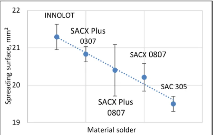
3.3 Result of spreading with different solder materials and paste quantity
A significant characteristic is observable in Fig. 8, which shows that the solder spread on the surface of the PCB could change significantly depending on the solder material (see Fig 10.).
Fig. 3. The effect of the material solder on the spreading of the solder
Here the different material composition of each solder is responsible for different spreading; the applied materials have also different melting points. Whenever the window of the solidus-liquidus is wider, the spreading surface increases. (This might be also explained by the variation of the heating factor of the reflowing profile. [14]). According to the previous researches, the flux may also facilitate rapid spreading [20]; in this experiment all the pastes were using the same general flux type (ROL0), however the proprietary composition (not necessary the activation parameter [21]) of different paste manufacturer products might alter the results. It is supposed, that the same flux is used in SACX and Innolot pastes (due to them being part of the same product family), so the cause of the difference enabled by the flux material can be ruled out overall, by the results shown in Fig 8.
The quantity of the solder paste has an effect on the spreading too (see Fig 9.). However the thickness change again does not seem to affect the spreading of the printed solder. The spreading surface is similar for both PCB thicknesses.
Fig. 9. The effect of the quantity of the solder on the spreading of the solder
19 20 21 22
Spreading surface, mm²
Material solder INNOLOT
SACX Plus 0307
SACX Plus 0807
SACX0807
SAC 305
10 12 14 16 18 20 22
1.6 1.8 2 2.2 2.4
Spreading Surface, mm²
Mask thickness, mm 2 mm of PCB thickness
17 18 19 20 21
1.6 1.8 2 2.2 2.4
Mask thickness, mm 1.5 mm of PCB thickness
3.4 Result of the VPS on the contact angle
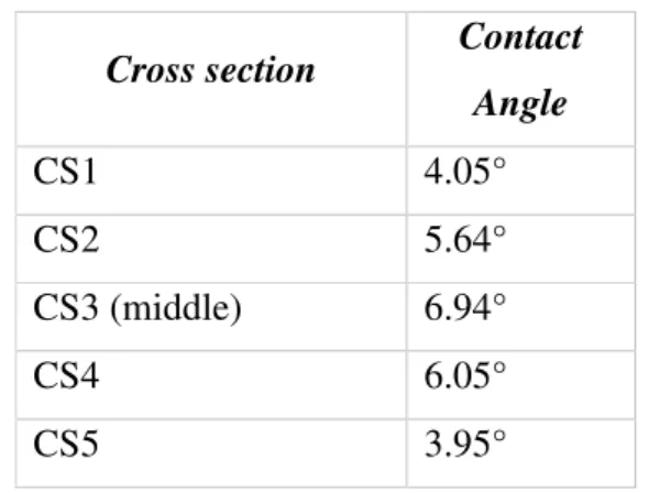
The result of the contact angle for five cross-section did not pass 7° (see Tab 2, Fig 10.). Knowing that small contact angles (<<90°) correspond to efficient wettability.
Tab. 2. The result of the sample cross section
Cross section Contact Angle
CS1 4.05°
CS2 5.64°
CS3 (middle) 6.94°
CS4 6.05°
CS5 3.95°
We conclude that the HL-VPS provides excellent wetting, compared to previous lead-free wetting experiments [13] without the observation of significant Sn haloing [23]. This result will be investigated further in future experiments with extended experiments.
Fig. 4. The movement of the contact angle in different level of cross-section
With the variation of the cross-sectioning planes, the highest angle is observable in the middle of the cut. This value can be considered as the only relevant result for the experiment. Also Figure 10. not only describes the importance of choosing a proper cross-section cut line for investigation, but with the complete cut line sweep, and the resulting characteristic, it was reaffirmed that the solder blob formed a
0 1 2 3 4 5 6 7 8
0 1 2 3 4 5 6
angle, °
cross section number
symmetrical circular shape. However it is also interesting to note that only ~2° absolute error was obtained by measuring the contact angle far from the middle point.
4.CONCLUSION
The quality and the efficiency of the soldering method or even the solder material can be tested with the wetting test. In this paper we investigated the effect of the VPS (HL-method) on the solder spreading and its contact angle.
To sum up, the experiments provided us with the following results:
The thickness of the FR4 based PCB does not have any considerable effect on the solder spreading.
The heating power does not have significant effect on the solder spreading, but minor increase was observed according to the increase of power.
The material of the solder can provide different spreading results (knowing that the volume of the solder and the heating process is the same).
The spreading of the solder depends substantially on the alloy and the melting point (liquidus- solidus window) of the solder material.
The HL-VPS can provide optimal contact angle between the PCB surface and the solder.
The cross-sectioning analysis shows regular shapes and excellent contact angles for the samples.
The investigation will continue in the future works, where the contact angles of different alloys, the effect of flux, the effect of different substrates with the impact of bigger thermal capacities will be evaluated on the solder.
ACKNOWLEDGEMENT
The research into the alloy composition and its effects of soldering quality is supported by the National Research, Development and Innovation Office – NKFIH, FK 127970.
The research into the effect of PCB substrates on the reflow process is supported by Pro Progressio.
The topic of vapour phase research is supported by the Stipendium Hungaricum Scholarship Programme (application ID: 166125) and the Bolyai János Scholarship - Bolyai+ (ÚNKP-18-4-BME- 321).
REFERENCES
[1] Zabel C. (2006) “Condensation Reflow Soldering - The Soldering Process with Solutions for future Technological Demands”, Germany, ASSCON Systemtechnik-Elektronik GmbH,
http://www.amtest.bg/press/Asscon/Vapour%20Phase%20Process.pdf (accessed at 10th January 2018.)
[2] Suihkonen D, “Vapor phase for lead-free reflow”, Global SMT & Packaging, Vol. 7, No. 9, (2007), pp. 30-32;
[3] Dusek, K. Busek, D., Placek, M. Geczy, A. Krammer, O. and Illes, B., “Influence of vapor phase soldering fluid Galden on wetting forces (tombstone effect)”, Journal of Materials Processing Technology, Volume 251. (2018), pp 20-25.
[4] “Galden® LS & HS Vapor Phase Soldering Fluids, Technical Data Sheet”,
www.solvay.cn/zh/binaries/Galden-LS-HS-Vapor-Phase-Soldering-Fluids_EN-220537.pdf, (accessed 2nd October 2018).
[5] Munroe, C, "Vapour phase vs. convenction reflow in RoHS compliant assembly" SMTA International Conference, Orlando, Florida, (2008), pp. 125-128.
[6] Dusek, K. and Urbanek, J, “Influence of the reduced oxygen concentration on the wetting force”, 29th International Spring Seminar on Electronics Technology, St. Marienthal, Germany, (2008), pp.
193-196,
[7] Guene, E, “Reliability study of No Clean chemistries for lead free solder paste in vapor phase reflow”, IEEE 18th Electronics Packaging Technology Conference, Singapore, (2016), pp 157-164;
[8] K.N. Prabhu, P. Fernandes,” Determination of Contact Angle of Various Fluids In oil Industry”, International Refereed Journal of Engineering and Science (IRJES), Vol 7, No. 1 (January 2018), pp. 61-63
[9] X. Zhao, M.J. Blunta, “Pore-scale modeling: Effects of wettability on waterflood oil recovery”, Journal of Petroleum Science and Engineering, Vol. 71, No. 3-4, (January 2010), pp. 169–178 [10] Wang YQ, Yang HF, Hang QG, Fang L, Ge SR. “Tribological and lubrication properties of
sandblast-textured surfaces with varied roughness”, Advanced Materials Research, Vols. 154-155 (October 2011), pp 1019-1022
[11] Y. Son, C. Kim, D.H. “Spreading of an Inkjet Droplet on a Solid Surface with a Controlled Contact Angle at Low Weber and Reynolds Numbers”, Langmuir, Vol. 24, No. 6, (October 2007), pp. 2900-2907
[12] National Center for Manufacturing Sciences Lead-Free Solder Project, Special Supplement to Surface Mount Technology, June 2000. NCMS Report 0401RE96, Lead-Free Solder Project, National Center for Manufacturing Sciences, Ann Arbor, MI, August 1997, June 1998.
[13] Olivér Krammer, László Puskás, Investigating the effect of nitrogen atmosphere on lead-free solder wetting angle, IEEE 17th International Symposium for Design and Technology in Electronic Packaging (SIITME), (2011), pp 159-162.
[14] Petr Veselý, Eva Horynová, Jiří Starý, David Bušek, Karel Dušek, Vít Zahradník, Martin Plaček, Pavel Mach, Martin Kučírek, Vladimír Ježek, Milan Dosedla, (2018) "Solder joint quality
evaluation based on heating factor", Circuit World, Vol. 44 Issue: 1, pp.37-44, https://doi.org/10.1108/CW-10-2017-0059
[15] Asscon DataSheet, Quicky 450 vapor phase soldering
https://www.asscon.de/e/pages/products/pdf/VP450_E_151104.pdf (10/03/2019)
[16] Nathan Barry, Lead-free Solders for High-Reliability Applications: High Cycle Fatigue Studies, 2008, University of Birmingham
[17] SketchAndCalc; https://www.microsoft.com/en-us/p/sketchandcalc-area- calculator/9n40104njj6n?activetab=pivot:overviewtab (10/12/2018) [18] Shesto UTFLU01 DataSheet
https://www.shesto.co.uk/uploads/general/files/Ultrasonic%20Cleaner%20UTFLU.PDF (10/12/2018)
[19] Isopropyl Alcohol (2-Propanol) DataSheet
http://www.labchem.com/tools/msds/msds/LC15750.pdf (10/12/2018) [20] Clarocit Powder DataSheet https://e-
shop.struers.com/US/EN/documents/40200074_Msds_US_English_59905583b6f46401c8f27d045b 97cde4.aspx (10/12/2018)
[21]V.H. López, A. R. Kennedy, “Flux-assisted wetting and spreading of Al on TiC”. Journal of Colloid and Interface Science, Vol. 298, No. 1, (2006), pp. 356–362.
[22] F. Cheng, F. Gao, J. Zhang, W. Jin, X. Xiao, “Tensile properties and wettability of SAC0307 and SAC105 low Ag lead-free solder alloys”. Journal of Materials Science, Vol. 46, No. 10, (2011), pp.
3424–3429
[23] Theron Lewis, Brian Chapman, Case Study Comparing the Solderability of a Specific Pb Free No Clean Paste in Vapor Phase and Convection Reflow, 2011. IPC APEX EXPO, Las Vegas, Nevada, USA