Investigation of the Microstructure of Mn-doped Tin-Silver-Copper Solder Alloys Solidified with Different Cooling Rates
Tamás Hurtony, Oliver Krammer, Balázs Illés, Péter Gordon
Budapest University of Technology and Economics, Department of Electronics Technology H-1111, Egry József u. 18., Budapest, Hungary
+36 1 463 4268, hurtony@ett.bme.hu
Abstract
Due to the moderate price and the non-toxicity, manganese is considered as an ideal dopant for the SAC (SnAgCu) solder alloys. Manganese refines the grain of solder joints, yielding better thermomechanical properties. In present research, the microstructure of the manganese- doped alloys solidified with different technological parameters had been investigated.
Sn/Ag0.3/Cu0.7 based solder alloy with three different Mn content (0.1, 0.4, 0.7% wt%) were reflowed on a copper substrate with tempered hot plate. They were solidified with different cooling rates from 0.3 to 4.5 K/s. Cross-sections have been prepared from the solder samples and the metallographic properties of the solder samples was investigated with optical and scanning electron microscopes. The characteristic features of the samples have been compared to conventionally used SAC305 (Sn/Ag3/Cu0.5) solder alloys, solidified with the same rates of cooling. Results showed that besides the grain refinement, the Mn content might also have effect on the evolution of intermetallic layer between the substrate and the solder alloy. The IMC grains of the layer were more elongated and more spalled grains had been observed close to the layer. However, independently of the cooling rate, the microstructure of the Mn containing solder alloys remained the same. This suggests that the macroscopic properties are also expected to be less sensitive to the cooling rate of the solidification.
Key words: lead-free soldering; manganese doping; cooling rate; selective electrochemical etching; scanning electron microscopy.
1. Introduction
The most common soldering technology for the automated, mass manufacturing of electronics devices is the reflow soldering technology [1] either by convection heating or by vapour phase [2,3].The restriction of hazardous substances urged the electronic industry to
ban the conventional lead-based solder alloys in the application of reflow soldering and to introduce the lead-free substitution of these materials. The change over was not easy; the appropriate set of the reflow profile became harder due to the narrower technological window [4], and the first generation of lead-free solder alloys were lagging behind the conventional eutectic solders in both mechanical and reliability properties. Nowadays, the most commonly applied second-generation alloy is the Sn-Ag-Cu (SAC). Huge number of researches is investigating the properties of SAC alloys, and according to them, the process parameters and the mechanical behaviours of some SAC solders are more superior compared to lead-bearing alloys. However in certain applications, for example under extreme operation, e.g.
overpressure [5] or extreme process environment [6], these improved solder alloys might not perform adequately; therefore the development of third generation lead-free solder alloys, even doped with microalloys (additives with less than 0.2 wt.%), or with nanoparticles is still a current topic.
The improved properties are pushed to the limit by adding minor alloying components (tracing elements) and/or nanoparticles into the SAC base solder in order to achieve e.g. better thermomechanical or drop-shock performance. As mentioned, one approach can be adding nanoparticles to the SAC solder alloy. Ani et al. added TiO2 and NiO nanoparticles, and they found that these additions can improve the wettability of the alloy, and can reduce the rate of growth of the intermetallic layer. The highest fillet height was observed by adding 0.01 wt%
NiO [7], and the lowest intermetallic layer thickness was reached by adding 0.05 wt.% TiO2
[8]. Thus, these reinforcing nanoparticles can enhance the quality and reliability properties of solder joints for ultra-fine package assembly.Due to the moderate price and the non-toxicity, the manganese is considered as an ideal dopant for the SAC solder alloys. Mn reported to have a grain refinement effect on the SAC solder alloys both in nanoparticle [9] and in micralloyed [10] form. At soldering temperature and below that the solubility of Mn in the Sn base solder alloy is relatively low; so even at very low concentration, Mn containing micro precipitation might appear inside the solder bulk which may act as a crystallization centre for the solidification of the SAC alloy. As the consequence of finer microstructure, these alloys might be more resistant against intensive and dynamic external mechanical exposure, such as drop tests [11]. The addition of minor composing element might also give the possibility to reduce the silver content of the SAC solder which might yield both in reliability increase [12]
and in significant cost reduction.
2. Materials and methods
The structural analyses and the measurement of intermetallic layer thickness was carried out for Sn/Ag0.3/Cu0.7 based solder alloys doped with 0.1, 0.4, 0.7 wt.% manganese and for a SAC305 (Sn/Ag3/Cu0.5) alloy as a reference. The solder bar had been pre-formed to solid solder wires with a diameter of 1 mm by cold forming wire process. The bumps were formed by cutting solder wires (⌀1 mm) to an exact length of 2 mm. This was achieved by preparing laser marks into the wire at equidistant positions. The solder preform had been cleaned with sonic bath in isopropanol. The solder preform had been reflowed on a 0.2 mm thick pure copper sheet which was previously cut into 15x5 mm substrates. In order to obtain relatively same geometry of the reflowed solder balls, solder mask was applied to prevent uncontrolled wetting by the solder balls. Kapton® tape was adhered onto the surface of the substrate and an exactly 900 µm diameter round aperture was cut on the mask also with laser. Four apertures had been formed on every substrate for reflowing the balls made from the four different alloys on the same substrate. This resulted in solder balls with approximately 2 mm in diameter, and with a solder substrate interface of 1.2 mm length at the symmetrical axis of the balls (Fig. 1).
Figure 1: The formed solder ball: a) optical microscopy image; b) cross-section
The application of such geometry provided high enough solder volume for not limiting the dissolution of the copper atoms into the molten solder, while the spherical shape of solder bump ensured the uniform heat distribution all over the solder interface. Furthermore the morphology of the intermetallic layer is expected to be similar in all direction.
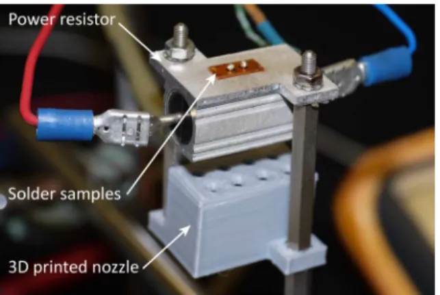
The solder balls had been reflowed on a custom made hot plate equipment. The heat was applied by a power resistor in order to have the minimal obtainable thermal inertia of the hot plate. Forced convectional cooling was applied to set the different cooling rates of the samples. A 3D printed nozzle was designed accommodating to the bottom of the power resistor to a fixed position (Fig. 2). The pressure of the blowing air was set by a regulator.
Thermal interface material was applied between the hot plate and the substrate, and the temperature was measured on the hot plate by thermocouples.
Figure 2: The custom made hot plate for preparing the solder ball samples with different cooling rate
The rates of cooling were set to 0.3, 2.5 and 4.5 K/s. The reflow profiles for cooling rates of are illustrated in Fig. 3.
Figure 3: The applied reflow profiles
Once the peak temperature of the hotplate (260 °C) was reached, the current load of the resistor was turned off and the air stream was released by a valve. The time needed for reaching the peak temperatures was approximately 2 minutes in every case. After melting the solders, they were in liquid form for at least 15 seconds before applying the cooling. As it can
be seen in Fig. 3., the temperature profiles of consecutive experiments were really similar to each other. The applied cooling rates of samples are reproducible. After the reflow soldering, the solder balls had been cross-sectioned. The microstructure of the solder joints and the thickness of the intermetallic layer inside them were analysed by scanning electron microscopy. Backscattered electron detector (BSE) was used for the structural analyses and EDX (energy-dispersive X-ray spectroscopy) was utilized for material composition measurements. The fine microstructure of the solder bulk had been revealed with a special selective electrochemical etching process [13].
3. Results
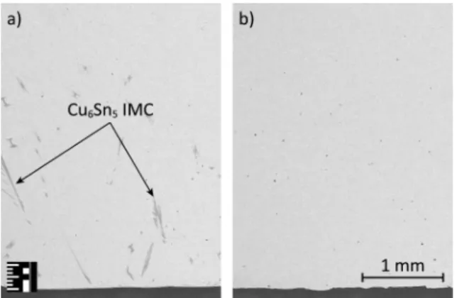
Due to the fact that no diffusion barrier layer was deposited onto the substrate significant copper dissolution was expected. The major part of the dissolved copper usually forms Cu6Sn5 intermetallic compound at the solder substrate interface but they can also crystalize inside the solder bulk. Higher amount of IMC was observed inside the solder bulk in the case of the slowly cooled samples (Fig. 4). This is because the total time above liquidus is higher, therefore higher amount of Cu atom can be dissolved into the solder bulk.
Figure 4: SEM micrographs of the SAC305 samples: a) solidified with 0.3 K/s; b) solidified with 2.5 K/s
The average thickness of the intermetallic layer was also slightly higher in the case of the slowly solidified samples (Fig. 5).
Figure 5: The intermetallic layers of the SAC305 samples: a) solidified with 0.3 K/s; b) solidified with 2.5 K/s
Due to the moderate cooling rate needle-like primary Cu6Sn5 IMCs had been formed inside the solder bulk (Fig. 6). Similar trend was observable in the case of all Mn containing samples, but the needle-like crystals of primary Cu6Sn5 IMCs were not such long as it was observed in the case of the SAC305 sample. The morphology of the intermetallic layer of both Mn containing and SAC305 solder samples were relatively similar to each other.
Continuous and scallop-type intermetallic layer was formed in the case of every sample.
However, the intermetallic layer of the 0.1 wt.% Mn containing solder were slightly different from the others. Independently of the cooling rate, the IMC grains of the layer were more elongated, and more spalled grains had been observed close to the layer in this sample.
Figure 6: The intermetallic layer of the SAC-Mn01 solder samples: a) solidified with 0.3 K/s; b) solidified with 2.5 K/s
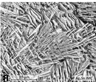
During the selective electrochemical etching process only the pure β-tin phases had been extracted from the cross-sectioning plane of the samples in a depth of approximately 50 µm. The dendritic arms of the tin phases had been extracted and the Ag3Sn intermetallic
compound remained in the interdendritic regions. They are forming a fibrous like network which strengthens the structure of the solder bulk. No plate-like primary Ag3Sn IMC had been observed on any of the samples (Fig. 7).
Figure 7: SEM micrographs of the SAC305 solder samples solidified with 0.3 K/s: a) before the selective etching; b) after the etching process
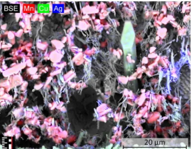
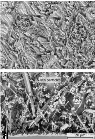
The manganese precipitates appears as granular features inside the solder bulk (Fig. 8).
These features act like nucleation centers for the Ag3Sn IMCs, therefore they are usually forming around the Mn particles.
Figure 8: Material composition map of a SAC-Mn04 solder sample. Mn precipitates are observable surrounded by Ag3Sn intermetallics.
Regardless of the cooling rate, the microstructure of the Mn containing solders was relatively similar to each other. The microstructure of the solder bulk containing any Mn was significantly different than that was observed in the case of SAC305 sample (Fig. 9). The Ag3Sn IMCs are also rather forming needle-like structures, and the presence of them is not restricted to any interdendritic region. In fact no dendritic structures of tin phases had been recognized inside the solder bulk of Mn containing solder. The Mn precipitations are most likely preventing the formation of regular β-tin dendrites.
Figure 9: SEM micrographs of the SACMn01 samples solidified with 2.5 K/s
Comparing the microstructure of the Mn containing solder close and relatively far from the substrate solder interface it can be observed that the relative abundance of manganese precipitates is significantly higher close to the interface. Since the density of the Mn atoms is only slightly higher than the density of the Sn this cannot be explained by the gravitational forces. More likely this is caused by the segregation of Mn precipitates during the solidification. Although the hot plate is cooled directly by the air stream, the solder balls are not solidifying from bottom to top. Because of the free convection they are also loosing heat from above, therefore the solidification of the balls are usually occurring from top to bottom and as the consequence of this the Mn are precipitates are segregating to the bottom of the solder.
Figure 10: SEM micrographs of SAC-Mn07 solder samples solidified with 0.3 K/s cooling rate: a) close to the solder-substrate interface; b) far from it
4. Conclusions
The microstructure of Mn containing solder alloy solidified with different cooling rate had been observed and compared to commercial SAC305 solder alloy. It was found that even 0.1 weight percent of Mn content can significantly alter the microstructure. Due to the grain refinement effect of the Mn particles inside the solder bulk, no β-tin dendrites can be formed and the Ag3Sn IMCs are not only present inside the interdenritic regions, but they are structurally distributed inside the solder.
Independently of the cooling rate of the solder samples the microstructure of the Mn containing solder alloys remained stationary. This suggests that the macroscopic properties are also expected to be less sensitive to the cooling rate of the solidification. Significantly higher amount of Mn particles had been observed close to the substrate of the solder which might be in correlation with the directionality of the solidification of the solder samples. As the solder is solidifying from top to the bottom the Mn particles are being segregated from the solution, and their concentration become higher close to the substrate.
Acknowledgements
This research was supported by the National Research, Development and Innovation Office – NKFIH, FK 127970.
References
[1] P. Veselý, E. Horynová, J. Starý, D. Bušek, K. Dušek, V. Zahradník, M. Dosedla, "Solder joint quality evaluation based on heating factor", Circuit World, Vol. 44, No. 1, pp. 37-44, 2018.
[2] A. Géczy, "Investigating heat transfer coefficient differences on printed circuit boards during vapour phase reflow soldering", International Journal of Heat and Mass Transfer, Vol. 109, pp. 167-174, 2017.
[3] L. Livovsky, A. Pietrikova, "Measurement and regulation of saturated vapour height level in VPS chamber", Soldering & Surface Mount Technology, early cite, 2019.
https://doi.org/10.1108/SSMT-10-2018-0040
[4] F. Steiner, V. Wirth, M. Hirman, "Relationship of Soldering Profile, Voids Formation and Strength of Soldered Joints", Proceedings of the 42nd International Spring Seminar on Electronics Technology (ISSE 2019), Wroclaw, Poland, May 15-19, 2019.
[5] W.Y.W. Yusoff, N. Ismail, N.S. Safee, A. Ismail, A. Jalar, M.A. Bakar, "Correlation of microstructural evolution and hardness properties of 99.0Sn-0.3Ag-0.7Cu (SAC0307) lead-free solder under blast wave condition", Soldering & Surface Mount Technology, Vol. 31, Issue 2, pp. 102-108, 2019.
[6] A. Geczy, M. Fejos, L. Tersztyánszky, "Investigating and compensating printed circuit board shrinkage induced failures during reflow soldering", Soldering & Surface Mount Technology, Vol. 27, Issue 2, pp. 61-68, 2015.
[7] F.C. Ani, A. Jalar, A.A. Saad, C.Y. Khor, M.A. Abas, Z. Bachok, N.K. Othman,
"Characterization of SAC – x NiO nano-reinforced lead-free solder joint in an ultra-fine package assembly", Soldering & Surface Mount Technology, Vol. 31, Issue 2, pp.109- 124, 2019.
[8] F.C. Ani, A. Jalar, A.A. Saad, C.Y. Khor, R. Ismail, Z. Bachok, M.A. Abas, N.K.
Othman, "SAC–xTiO2 nano-reinforced lead-free solder joint characterizations in ultra- fine package assembly", Soldering & Surface Mount Technology, Vol. 30, Issue 1, pp. 1- 13, 2018.
[9] Y. Tang, S. Luo, G. Li, Z. Yang, C. Hou, "Effects of Mn nanoparticle addition on wettability, microstructure and microhardness of low-Ag Sn-0.3Ag-0.7Cu-xMn(np)
composite solders", Soldering & Surface Mount Technology, Vol. 30, Issue 3, pp. 153- 163, 2018.
[10] L.W. Lin, J.M. Song, Y.S. Lai, Y.T. Chiu, N.C. Lee, J.Y. Uan, "Alloying modification of Sn–Ag–Cu solders by manganese and titanium", Microelectronics Reliability, Vol. 49, pp. 235-241, 2009.
[11] W. Liu, N.C. Lee, A. Porras, M. Ding, A. Gallagher, A. Huang, S. Chen, J.C.B. Lee,
"Achieving high reliability low cost lead-free SAC solder joints via Mn or Ce doping", Electronic Components and Technology Conference, pp. 994-1007, 2009.
[12] B. Medgyes, E. Roman, A. Bohnert, S. Szurdán, X. Zhong and G. Harsányi,
"Electrochemical Migration Investigations on SAC-Bi-xMn Solder Alloys", 2018 IEEE 24th International Symposium for Design and Technology in Electronic Packaging (SIITME), Iasi, pp. 80-212, 2018.
[13] T. Hurtony, A. Bonyár, P. Gordon, G. Harsányi, "Investigation of intermetallic compounds (IMCs) in electrochemically stripped solder joints with SEM", Microelectronics Reliability, Vol. 52, pp. 1138-1142, 2012.