Establishing a Machine-learning Based Framework for Optimising Electronics Assembly
Oliver Krammer, Tareq I. Al-Ma’aiteh, Péter Martinek and Attila Géczy
Budapest University of Technology and Economics
Department of Electronics Technology, Faculty of Electrical Engineering and Informatics, Budapest, Hungary krammer@ett.bme.hu
Abstract: By the spread of miniaturized components, like the 0201mm size-code (200 × 100 µm) passives, utilizing advanced optimization techniques becomes crucial in this field. A framework was established, which used machine-learning-based estimators to predict the yield of any manufacturing process in electronics technology. The framework includes using various methods, like artificial neural networks (ANN), decision trees and neuro-fuzzy inference systems. It can automatically split the input data into training and testing sets for each learning epoch to reach optimal performance and prevent possible overfitting at the same time. Besides, optimal structures and description functions are also determined automatically. To assess the prediction error, the framework calculates the MAE (Mean Absolute Error), the RMSE (Root Mean Square Error) and the MAPE (Mean Absolute Percentage Error) parameters to decide if the built estimator structure is appropriate. As an outcome, the framework can provide several parameters that the user can optionally select. Parameters like the predicted values of a process output parameter over different input process parameters are provided.
Besides, KPI (Key Process Index) of the output parameters or the Desirability Function (which combines many output parameters) can be acquired. The applicability and the performance of the framework were analyzed on the stencil printing process by building an ANN structure.
1. INTRODUCTION
Enhancing the yield of electronics assembly processes is always in the focus of researchers working in electronics packaging technology. By the spread of miniaturized components, like the 0201mm size-code (200 × 100 µm) passives, utilizing advanced optimization techniques becomes crucial in this field. These components are assembled by reflow soldering technology [1–3] onto the printed circuit board (PCB), where the most crucial step is stencil printing [4]. Soldering failures of 50–60% originates from the defects of this process, like solder paste skipping or solder paste bridging. Typical soldering failures in these cases can be the formation of open joints or solder bridges and the shift of the components from their proper location on the PCB [5].
Many researchers dealt with the optimization of stencil printing. Edwards showed in 1994 that the early- phase optimization of this process can significantly improve its first-pass yield [6]. In the beginning, empirical optimization methods were readily used like the Taguchi or the DMAIC (Define, Measure, Analyse, Improve and Control) methods. Then, methods based on either numerical modelling or machine-learning have spread to optimize electronics assembly processes. Wu classified solder joints by using the techniques of decision trees and random forests [7]. These methods' classification performances were 98.9% and 100%, respectively, in the test scenario. Tsai analyzed the process of stencil printing by utilizing artificial neural networks (ANN) [4]. They could predict the deposited volume of the solder paste and the solder joints' subjective quality with a 5–8% error.
Though they did not assess the apertures' size by their area ratio (AR), but they analyzed only some distinct component types (QFP with pitch-size of 0.63, 0.5, 0.4 mm). Similar results were achieved by using neuro-fuzzy and fuzzy-logic-based Taguchi methods to optimize the stencil printing process. Up to now, none of the recent research works dealt with complex estimator systems, which can flexibly assess electronics manufacturing processes. Besides, the stencil printing process analyses also lacked some key input parameters, like the size of
the stencil apertures described by their area ratio, or the statistical parameters of the particle size distribution in solder pastes.
2. MATERIALS AND METHODS
A framework was established, which includes an ANN-based (Artificial Neural Network) estimator structure.
Users can freely optimize any of their processes by providing an input database for training purposes. Users can define a set of output parameters also. After providing the set of data, the framework carries out an automatic optimization of the ANN structure using different training methods, as detailed below.
ANN models include artificial neurons, which receive and forward signals from the input till the output. The neurons in the models are arranged into (hidden) layers, and the structure is defined in a strict order; that is, a neuron can only communicate with those in a neighboring layer (Fig. 1).
Fig. 1. The general structure of an ANN-based predictor.
The activation function of a node can formally be described by the following expression (1) [8]:
(
−1)
=
+l l l l
j jk k j
k
z w a b (1)
where zlj is the input of the j-th neuron in the layer l, akl−1 is the output value of the k-th neuron in the layer l–1,
l
wjk is a weighting parameter defined between these two neurons, and bj is a bias factor for the j-th neuron. After determining the structure of the ANN, the next step is the training by a set of data for tuning the weighting and bias parameters. A widespread training method is the so-called Bayes regularization (BR) for defining the weighting parameters in an iterative manner [9]. Though the BR method can provide excellent results, predictions with low errors, the training time can be extensive. The other widespread training method is the so- called Levenberg-Marquardt, which relies on the fitting of smallest squares approach [10]. This can provide predictions with a reasonably low error by a much shorter training time. The created framework can apply both these training methods by choice of the user. After selecting the training method, the framework carries out the automatic fine-tuning of the ANN structure by testing the predicted values to the ones in the training dataset. The accuracy of the prediction is characterized by numerous parameters, like the RMSE (root-mean-square error), MAE (mean absolute error), MAPE (mean absolute percentage error). Finally, summarizing parameters can be selected to be calculated, providing an overview for many process output parameters in one value; these include the Key Process Index (KPI) (2) and the Desirability Function (DF) (3) [11].
1 / and
= − − =
i i i i i i
KPI µ y) µ KPI w KPI
(2)
where KPIi is the index for the i-th output parameter, µi is the target of the i-th parameter, y)i is the estimator (mean) of the i-th parameter, and wi is a weight parameter for the summation of KPIi-s.
(
1 2)
1/0
and ...
−
−
−
= −
=
s
i i
i i i
i i
t
i i
i i i i
i i
k k
y LSL
LSL y µ
µ LSL
y USL
d µ y USL
µ USL
Otherwise
DF d d d
) )
) )
(3)
where di is the desirability value of a single output parameter, USLi and LSLi are the upper and lower specification limits, and s and t are weighting factors.
The framework was tested on the process of stencil printing. The training database was created by empirical methods to test the framework. For the input dataset, different types of solder pastes (Type-3, Type-4, Type-5) were deposited through apertures with varying sizes at different printing speeds (from 20 mm/s to 120 mm/s).
The dimensions of the apertures were characterized by their area ratio (ratio between the area and the wall- surface), and they were varied between 0.35 and 1.7. The output data vector included the area, the height, and the volume of the deposits. By the predicted values, the KPI and DF were calculated.
3.RESULTS
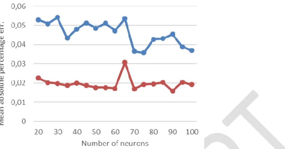
The framework was trained by LM method at first for predicting the quality of stencil printing. The ANN structure consisted of one hidden layer. During the automatic fine-tune of the structure, the number of the hidden neurons was varied between 10 and 100. The framework split the input database into training and testing sets automatically. More than one training cycles were performed since the split into the training and test sets is random. Thereby, the average prediction capability (characterized by the MAPE parameter) of the ANN structure could be addressed. The average values and the deviation of the MAPE are illustrated in Fig. 2., whereas the training time is presented in Fig. 3.
Fig. 2. MAPE of the ANN prediction over the number of neurons by LM training (blue: average MAPE; red: deviation of the MAPE).
Fig. 3. Training time over the number of neurons.
The best prediction accuracy, the lowest MAPE, was obtained at a neuron number 85, with a reasonably low training time. The average MAPE value was 3.6%, in which the prediction error was the lowest for the deposited solder paste thickness (2.2%). The prediction errors for the deposited area and volume were slightly larger, 3.8%
and 4.8%, respectively. A significant decrease in the prediction error could not have been reached either with much longer training times based on the experiments.
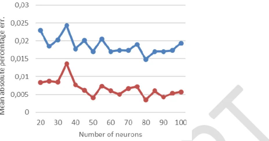
The ANN structure was trained utilizing also the BR training method. The MAPE values and the training times are presented in Fig. 4 and 5.
Fig. 4. MAPE of the ANN prediction over the number of neurons by BR training (blue: average MAPE; red: deviation of the MAPE).
Fig. 5. Training time over the number of neurons.
The best prediction error was obtained at the neuron number 80. The average MAPE was 1.5% in this case;
the MAPE for predicting the area, thickness and volume of the deposited solder pastes were 1.3%, 1.2%, 1.9%, respectively. At the same time, the training time was much longer, reached eve 5–10 minutes. For specific cases, specific processes, users can set thresholds either for the desired MAPE or the training time, and the framework can utilize the appropriate training method; that is, the LM method is slightly less accurate but faster, the BR method more accurate, but slower.
After the successful training, the ANN predicted the expected transfer efficiency over the size of apertures (described by the area ratio). The measured and predicted values are illustrated in Fig. 6; the predicted values are in the proximity of the measured ones at all aperture sizes.
Fig. 6. ANN predicted transfer efficiency; acceptance by mean (green arrow), or 1st quartile (orange arrow).
Exciting question if the acceptance limit should be set for the mean of the efficiency or the first quartile, which would stand a stricter requirement against the process. Note that the transfer efficiency can extend 100%.
The reason is that slight air gaps can exist between the stencil and the printed circuit board, yielding thicker paste deposits than the thickness of the stencil and thereby producing deposits with a larger volume than the volume of stencil aperture.
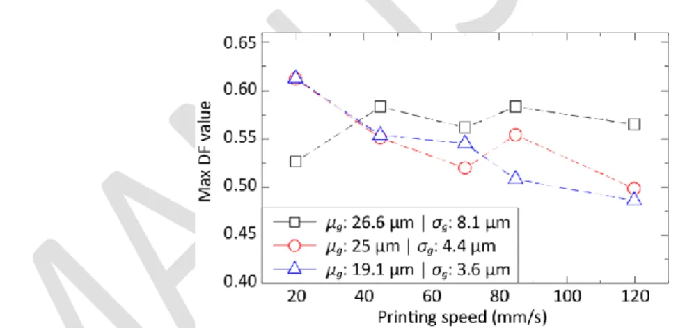
Then, the DF (consisting of the output parameter space) was also calculated for the different printing speeds and solder paste types (Type-3 – µg = 26.6 µm; Type-4 – µg = 25 µm; Type-5 – µg = 19.1 µm). The obtained DF values are illustrated in Fig. 7. In the investigated case, the highest DF values were obtained at the printing speed of 20 mm/s for the Type-4 and Type-5 solder pastes. The highest DF value for the Type-3 solder paste was reached at the printing speed of 45 mm/s. The DF values extended 50% for all the investigated cases. By analyzing DF plots, one can determine an optimal printing speed (or any process parameter), considering the desired throughput of the manufacturing line and an acceptable value of DF.
Fig. 7. DF over the printing speed and the various types of solder pastes (µg and σg are the geometric mean and SD of the particle sizes).
4.CONCLUSION
A framework was established, which used machine-learning-based estimators to predict the yield of any manufacturing process in electronics technology. An appropriate predicting capability was obtained for the process of stencil printing by testing the applicability of the framework. By using the proposed framework, process optimization can be performed on a daily basis, and the yield can be enhanced significantly.
ACKNOWLEDGEMENT
This paper was supported by the János Bolyai Research Scholarship of the Hungarian Academy of Sciences.
Supported by the ÚNKP-20-5 New National Excellence Program of the Ministry for Innovation and Technology from the source of the National Research, Development and Innovation Fund. The research was partially supported by the project “FK 132186” of NRDI Office. The research reported in this paper and carried out at the BME has been partially supported by the NRDI Fund based on the charter of bolster issued by the NRDI Office under the auspices of the Ministry for Innovation and Technology.
REFERENCES
[1] B. Illés, "Comparing 2D and 3D numerical simulation results of gas flow velocity in convection reflow oven", Soldering & Surface Mount Technology, Vol. 26, No. 4, 2014, pp. 223–230.
[2] B. Illés, G. Harsányi, "Investigating direction characteristics of the heat transfer coefficient in forced convection reflow oven", Experimental Thermal and Fluid Science, Vol. 33, 2009, pp. 642–650.
[3] B. Illés, I. Bakó, "Numerical study of the gas flow velocity space in convection reflow oven", International Journal of Heat and Mass Transfer, Vol. 70, 2014, pp. 185–191.
[4] T.N. Tsai, "Modeling and optimisation of stencil printing operations: A comparison study", Comput. Ind. Eng., Vol. 54, No. 3, 2008, pp. 374–389.
[5] B. Illés, G. Harsányi, "3D Thermal Model to Investigate Component Displacement Phenomenon during Reflow Soldering", Microelectronics Reliability, Vol. 48, 2008, pp. 1062–1068.
[6] K.L. Edwards, "Towards more effective decision support in materials and design engineering", Mater. Design, Vol. 15, No. 5, 1994, pp. 251–258.
[7] H. Wu, "Solder joint defect classification based on ensemble learning", Solder. Surf. Mt. Tech., Vol. 29, No. 3, 2017, pp. 164–170.
[8] T. Hastie, R. Tibshirani, J.H. Friedman, "The Elements of Statistical Learning – Data Mining, Inference, and Prediction", Springer-Verlag, 2 ed., 2009. ISBN-10: 0387848576
[9] D.J.C. MacKay, "Bayesian interpolation", Neural Comput., Vol. 4, 1992, pp. 415–447.
[10] M.T. Hagan, M.B. Menhaj, "Training feedforward networks with the Marquardt algorithm", IEEE Trans. Neural Netw., Vol. 5, 1994, pp. 989–993.
[11] G. Derringer, R. Suich, "Simultaneous Optimization of Several Response Variables", Journal of Quality Technology, Vol. 12, No. 4, 1980, pp. 214–219.