Predicting the Transfer Efficiency of Stencil Printing by Machine Learning Technique
Oliver Krammer, Tareq Al-Ma’aiteh, Péter Martinek, Krisztián Anda, Norbert Balogh
Department of Electronics Technology
Budapest University of Technology and Economics, Budapest, Hungary krammer@ett.bme.hu
Abstract:Experiment was carried out for acquiring data regarding the transfer efficiency of stencil printing, and a machine learning-based technique (artificial neural network) was trained for predicting that parameter. The input parameters space in the experiment included the printing speed at five different levels (between 20 and120 mm/s) and the area ratio of stencil apertures from 0.34 to1.69.
Three types of lead-free solder paste were also investigated as follows: Type-3 (particle size range is 20–45 µm), Type-4 (20–38 µm), Type-5 (10–25 µm). The output parameter space included the height and the area of the print deposits and the respective transfer efficiency, which is the ratio of the deposited paste volume to the aperture volume. Finally, an artificial neural network was trained with the empirical data using the Levenberg–Marquardt training algorithm. The optimal tuning factor for the fine-tuning of the network size was found to be approximately 9, resulting in a hidden neuron number of 160. The trained network was able to predict the output parameters with a mean average percentage error (MAPE) lower than 3%. Though, the prediction error depended on the values of the input parameters, which is elaborated in the paper in details. The research proved the applicability of machine learning techniques in the yield prediction of the process of stencil printing.
1. INTRODUCTION
The more sophisticated electronic devices raise the need for such assembly technologies, which capable of reaching zero-defect manufacturing. This is aided by the intelligent manufacturing in the view of Industry 4.0. The basic concept of Industry 4.0 includes industrial IoT (internet of things), machine-to- machine-interaction and process optimisation by machine learning techniques, which utilises the data collected by the intelligent manufacturing equipment.
Stencil printing is one of the crucial steps in reflow soldering technology. Many of the soldering failures, like bridging or open joints, can be originated from this process. The most critical parameters, which are affecting the yield of the stencil printing process are the rheology of the solder paste, the printing parameters (pressure, speed etc.), and the quality and size of the stencil apertures. That is the reason for intensive analyses of solder paste rheology on the one hand. Pietriková and Kravcik showed for example that the viscosity of solder pastes decreases significantly over increasing rates of shear [1,2]; suggesting that the
printing speed is a noteworthy affecting parameter regarding the yield of stencil printing. Rheology of solder pastes was addressed too by Barbosa et al., finding that the non-Newtonian behaviour of solder pastes could originate from the properties of flux [3].
The flux is responsible for removing the contamination from the metallization to be soldered.
Its additional role is preventing oxidation before and during the soldering process. Environmental conditions during the soldering have a substantial effect on the quality and reliability of solder joints. As a consequence, Asghar et al. approached defect minimisation and process improvement of stencil printing via a comparative study [4]. They found that both insufficient solder paste printing and paste bridging can occur in printing when the PCB (Printed Circuit Board) pads are oxidised or the stencil is contaminated. Yu et al. addressed the cycle time of stencil cleaning by a discrete-time, discrete-state homogeneous Markov chain [5]. A stencil cleaning decision model based on renewal reward theorem was established, and the optimal cleaning time was obtained through a balance between quality loss and the loss on idle time.
Similar soldering problems can arise if the particles in the solder paste are oxidised, that is why a monolayer surface coating of stearic acid was developed by Peng et al. to increase the anti-oxidation property of solder pastes [6]. Further improvements and process optimisation in this field can be obtained, e.g. by utilising the advantages of Industry 4.0 concept and the extensive capability of machine learning techniques.
Investigating machine learning techniques is recently in focus in several fields of electronics manufacturing, since more and more data available from the manufacturing processes, and machine learning techniques are superior in the optimisation of non-linear procedures. For example, the efficiency of pin-in-paste technology was addressed by Martinek et al. [7]. Machine learning framework for predicting the reliability of solder joints was presented by Yi and Jones [8]. It was applied to predict the long-term reliability of lead-free Sn96.5Ag3.0Cu0.5 (SAC305) joints for three commonly used surface-finishes such OSP (organic solderability preservative), ENIG (electroless nickel and immersion gold) and ImAg (immersion silver). The obtained results showed that the predicted failure based on the machine learning method was much more accurate than that of the Weibull method. Huang et al. used data mining methodology too to establish an intelligent decision system for the assembly process of PCBs [9].
However, the small-form passive components and ultra-fine pitch integrated circuits demand further process optimisation of stencil printing for surface mounted components by machine learning techniques.
2. MATERIALS AND METHODS
For predicting the transfer efficiency of the stencil printing, an ANN (artificial neural network) based approach has been established, which the training and testing data set was obtained by experiments.
2.1. Experimental
The research was carried out focusing on the transfer efficiency of stencil printing, which is one of the most significant characterising parameters of this process. The transfer efficiency of stencil printing (ratio of the deposited paste volume to the aperture volume) depends mainly on four parameters: rheology of the solder paste, process capability of the stencil printer, stencil manufacturing technology (e.g. laser-
cutting or electroforming), and the size of the stencil aperture. The size of the aperture is usually characterised by its area ratio (1) [10]:
2 AR w l
w l t
(1)
where w is the shorter side of the aperture, l is the longer side, and t is stencil foil thickness.
For investigating the transfer efficiency, and for obtaining the ANN training data, the transfer efficiency of stencil printing has been determined for different printing speeds (20, 45, 70, 85 and 120 mm/s), for different types of solder paste and for stencil apertures with varying area ratios. Further printing parameters were: specific squeegee force was 90 N, and the stencil separation speed was 10 mm/s. A test stencil has been designed, where the area ratio of the apertures ranged between 0.34 and 1.69. The stencil was made from stainless steel with laser- cutting. Its thickness was 150 µm.
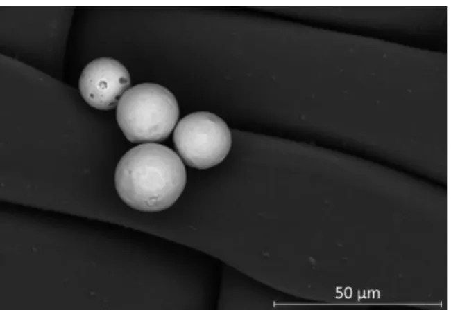
The different types of solder pastes in the experiment included Type-3, Type-4 and Type-5. All the solder pastes had the same flux vehicle to exclude the effect of flux rheology from the analysis. The theoretical particles sizes were 25–45 µm, 20–38 µm and 15–25 µm, respectively. Though, for acquiring detailed information regarding the solder paste, the particle sizes were measured in each solder paste by scanning electron microscopy images (Fig. 1).
Fig. 1. Scanning electron microscopy image of a Type-5 solder paste (theoretical particle size 10–25 µm).
The particle size distribution was characterised with log-normal parameters, like the geometric mean (eµ) and geometric standard deviation (eσ). With this characterisation, the ANN could be trained with quantitative parameters of the solder paste, instead of
the qualitative parameters, like Type-3-4-5. The log- normal fittings on the particle sizes in the different solder pastes are illustrated in Fig. 2. The obtained parameters are collected in Table 1.
Table 1. Log-normal parameters of particle diameters
Paste type Type-3 Type-4 Type-5
Geom. mean (µm) 26.6 25 19.1
Geom. SD (µm) 8.1 4.4 3.6
Fig. 2. Log-normal fittings on particle size distributions in solder pastes.
The transfer efficiency of stencil printing and the thickness and area of paste deposits were measured with an automated SPI (solder paste inspection) for each aperture and each experimental parameter (Fig.
3). The whole experiment consisted of 75 test runs (5 levels of printing speed, 3 levels of solder paste type and 5 repeats of measurements), and solder paste deposits at 209 locations were analysed in each run.
The experiment resulted in 15 675 vectors of the input and output parameters.
Fig. 3. Automated measurement of solder pastes deposits (AR: 0.42 → TE: 53%; area: 82%; thickness: 97 µm).
2.2. The ANN method
An artificial neural network was used to predict all the output data (transfer efficiency, thickness, area) for any input parameters. To minimise the prediction error, the optimal structure parameters were determined for the network. One hidden layer was applied for calculating the height of the print deposits and the respective transfer efficiency as a function of the printing speed, the aperture size and the solder paste type. The optimal number of hidden neurons was approached by (2):
dim( ) dim( )
N S
I O (2)
where N is the optimal number of hidden neurons, S is the number of samples in the training data set, I is the input data, O is the output data, dim(I) and dim(O) are the dimensions of the input and output vector spaces respectively, and α is a tuning factor between 2 and 10 [11].
The Levenberg–Marquardt training algorithm was applied for the training of the neural network. This was able to define desired operating parameters in significantly lower processing time – using other algorithms may consume enormous time for the training because the number of input samples and the size of the neural network is quite large [12].
Experimental data were split into a training set and a test set, where the number of samples was 70 and 30%
of the original data set respectively. Stochastic subsampling was also applied to enhance training performance.
The mean average percentage error (MAPE) was calculated for the predicted output (volume, area and thickness of deposited solder paste) of multiple trained networks. The optimal tuning factor was found to be approximately 9, resulting in a hidden neuron number of 160 (Fig. 4). The training time was 586 s in this case (Fig. 5). Neural networks with even lower prediction errors could have been found, but with significantly higher training times; the training time increased gradually up to 3300 s. Based on the preliminary test, the optimal neural network (the network with the lower MAPE value for relatively short training time) was found and used for further prediction of the height of the print deposits and the respective transfer efficiency as a function of the printing speed and the solder paste type.
Fig. 4. Mean absolute percentage error of the output parameters as a function of neuron number.
Fig. 5. Training time as a function of neuron number.
3.RESULTS
As mentioned, during the training, the prediction error (MAPE) against the test data was 2.9% for the prediction of the transfer efficiency over the area ratio, 1.5% for the prediction of the height and 5.5% for the volume, respectively. After the training, the prediction error was analysed further in details. The predicted values of transfer efficiency over the area ratio was examined for all the printing speeds and paste types.
As an example, Fig. 6. illustrates the examination for the printing speed of 45 mm/s and Type-4 (particle properties: eµ = 25 µm; eσ = 4.4 µm) solder paste. The empirical results proved the well-known rule that acceptable print quality (e.g., transfer efficiency over 75%) can be expected over the aperture area ratio 0.66. The ANN predicted values of transfer efficiency (represented by a blue line in Fig. 6.) felt within the range of measurement results over the whole measured range of aperture area ratio. This result proved for these values of input parameters the applicability of machine learning techniques for the characterisation of the stencil printing process.
Fig. 6. Transfer efficiency of the Type-4 solder paste at a
printing speed of 45 mm/s.
Next, the mean absolute percentage error for different values of input parameters has been analysed.
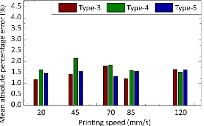
Fig. 7. illustrates these percentage errors for the output (predicted) parameter of the deposited area as a function of printing speed in paste type. It was found that the prediction error did not depend significantly on the printing speed or the type of solder paste. In the case of Type-5 solder pastes, the prediction error was slightly higher, but its relative value was still below 4 per cent.
Fig. 7. Mean absolute percentage error of predicting deposited area of solder pastes.
The similar capability of the ANN-based prediction method was found for the predicted values of deposited paste thickness (Fig. 8). The prediction error for this output parameter was even lower, laid below
~2% for all the values of input parameters. Finally, the prediction capability was analysed for the output parameter of transfer efficiency (Fig. 9). Slightly higher prediction error was observed for this output parameter, which might have originated from the somewhat higher uncertainty of the transfer efficiency.
Note that the transfer efficiency includes the uncertainty of both the deposited area and thickness.
Fig. 8. Mean absolute percentage error of predicting deposited thickness of solder pastes.
Fig. 9. Mean absolute percentage error of predicting transfer efficiency of solder pastes.
The results of all three output parameters showed that the prediction capability of the artificial neural network is quite stable over the examined input parameter range.
4. CONCLUSIONS
An experiment was carried out for acquiring data regarding the yield of stencil printing (transfer efficiency, area and thickness), and a machine learning-based technique (artificial neural network) was trained by Levenberg–Marquardt training algorithm for predicting those parameters. The prediction error of these output parameters was lower than 4 per cent for many values of input parameters, like printing speed, type of solder paste, area ratio of stencil apertures. The results proved the applicability of machine learning techniques in predicting the yield of electronics manufacturing processes, like stencil printing. These predictions can be used both for early phase and continuous process optimisations and can result in the reduction of costs of introducing new products into the electronics manufacturing.
ACKNOWLEDGEMENT
This paper was supported by the János Bolyai Research Scholarship of the Hungarian Academy of Sciences.
Supported by the ÚNKP-19-4 New National Excellence Program of The Ministry of Human Capacities.
The research reported in this paper was supported by the Higher Education Excellence Program of the Ministry of Human Capacities in the frame of Artificial Intelligence research area of Budapest University of Technology and Economics (BME FIKP-MI/SC).
The research was supported by the Pro-Progressio Foundation
REFERENCES
[1] Author One, Author Two, "Title of Paper", Source, Vol. 17, No. 4, month year, pp. First page-last page.
[1] A. Pietriková, M. Kravcik, "Investigation of rheology behavior of solder paste", 35th International Spring Seminar on Electronics Technology, Bad Aussee, 2012, pp. 138-143.
[2] A. Pietriková, M. Kravcik, "Boundary value of rheological properties of solder paste", 34th International Spring Seminar on Electronics Technology, Tatranska Lomnica, 2011, pp. 94-97.
[3] F. Barbosa, J. Teixeira, S. Teixeira, R. Lima, D. Soares, D. Pinho, "Rheology of F620 solder paste and flux", Soldering & Surface Mount Technology, Vol. 31, No.
2, 2019, pp. 125-132.
[4] R. Asghar, F. Rehman, A. Aman, K. Iqbal, A. Nawaz,
"Defect minimisation and process improvement in SMT lead-free solder paste printing: a comparative study", Soldering & Surface Mount Technology, Vol.
32, No. 1, 2019, pp. 1-9.
[5] J. Yu, L. Cao, H. Fu, J. Guo, "A method for optimising stencil cleaning time in solder paste printing process", Soldering & Surface Mount Technology, Vol. 31, No.
4, 2019, pp. 233-239.
[6] F. Peng, W. Liu, Y. Huang, S. Tang, C. Liang, Y. Ma,
"Effect of stearic acid coating on anti-oxidation property of Sn-Ag-Cu solder powder", Soldering &
Surface Mount Technology, Vol. 31, No. 1, 2019, pp.
68-74.
[7] P. Martinek, O. Krammer, "Analysing machine learning techniques for predicting the hole-filling in pin-in-paste technology", Comput. Ind. Eng., Vol. 136, 2019, pp. 187-194.
[8] S. Yi, R. Jones, "Machine learning framework for predicting reliability of solder joints", Soldering &
Surface Mount Technology, Vol. 32, No. 2, 2019, pp.
82-92.
[9] C. Huang, M. Ruano, C. Chen, C. Greene, "Applying data mining methodology to establish an intelligent decision system for PCBA process", Soldering &
Surface Mount Technology, Vol. 31, No. 4, 2019, pp.
271-278.
[10] T.N. Tsai, "Modeling and optimisation of stencil printing operations: A comparison study", Comput. Ind.
Eng., Vol. 54, No. 3, 2008, pp. 374-389.
[11] K.G. Sheela, S.N. Deepa, "Review on Methods to Fix Number of Hidden Neurons in Neural Networks", Mathematical Problems in Engineering, 2013, pp. 1- 11.
[12] M.T. Hagan, M.B. Menhaj, "Training feedforward networks with the Marquardt algorithm", IEEE Trans.
Neural Netw, Vol. 5, 1994, pp. 989-993.