Applied Surface Science 548 (2021) 149275
Available online 9 February 2021
0169-4332/© 2021 The Authors. Published by Elsevier B.V. This is an open access article under the CC BY license (http://creativecommons.org/licenses/by/4.0/).
Full Length Article
Material proposal for 2D indium oxide
Anelia Kakanakova-Georgieva
a,*, Filippo Giannazzo
b, Giuseppe Nicotra
b, Ildik ´ o Cora
c, Gueorgui K. Gueorguiev
a, Per O.Å. Persson
a, B ´ ela P ´ ecz
caDepartment of Physics, Chemistry and Biology (IFM), Link¨oping University, 581 83 Link¨oping, Sweden
bConsiglio Nazionale delle Ricerche, Istituto per la Microelettronica e Microsistemi, Strada VIII, n. 5, Zona Industriale, I-95121 Catania, Italy
cCentre for Energy Research, Institute of Technical Physics and Materials Science, Konkoly-Thege M. út 29-33, Budapest 1121, Hungary
A R T I C L E I N F O Keywords:
2D oxides
Metal organic chemical vapor deposition Conductive atomic force microscopy Scanning transmission electron microscopy
A B S T R A C T
Realization of semiconductor materials at the two-dimensional (2D) limit can elicit exceptional and diversified performance exercising transformative influence on modern technology. We report experimental evidence for the formation of conceptually new 2D indium oxide (InO) and its material characteristics. The formation of 2D InO was harvested through targeted intercalation of indium (In) atoms and deposition kinetics at graphene/SiC interface using a robust metal organic chemical vapor deposition (MOCVD) process. A distinct structural configuration of two sub-layers of In atoms in “atop” positions was imaged by scanning transmission electron microscopy (STEM). The bonding of oxygen atoms to indium atoms was indicated using electron energy loss spectroscopy (EELS). A wide bandgap energy measuring a value of 4.1 eV was estimated by conductive atomic force microscopy measurements (C-AFM) for the 2D InO.
1. Introduction
Expansion of fundamental scientific knowledge supported by development of theoretical approaches, deposition strategies, and advanced characterization drives rational design of materials at nano- scale. This is recognized as a materials science platform that brings about conceptually new performance with well-established semi- conductor materials which have been subjected to a variety of nano- structures. Nanostructures such as two-dimensional quantum wells, one- dimensional quantum wires/rods, and zero-dimensional quantum dots can be stated as being among the most typical examples. At least one dimension of the nanostructure is limited by the exciton Bohr radius, e.
g., ~ 8 nm for indium nitride (InN), as compared to 2.4 nm for GaN, and 1.4 nm for AlN in the material system of group III nitrides [1]. Indium oxide (In2O3) from the material system of group III sesquioxides [2]
provides an extra compelling example. In addition to the realization of quantum confinement effects, one-dimensional nanostructures repre- sented by nanowires with diameters below 4 nm greatly promote the performance of chemical- and biosensors, and transparent electronics [3]. An array of obliquely aligned InN nanowires has been demonstrated for the fabrication of efficient nanogenerators to convert mechanical energy into electricity [4].
Exceptional and diversified performance of modern-technology-
relevant indium nitride and indium oxide might further be elicited through their realization at the 2D limit. Unlike some other materials, 3D group III nitrides and group III sesquioxides are not naturally layered materials. However, a case of kinetically stabilized 2D InN can be explored within the material concept for ultrathin “graphitic-like” films of group III nitrides [5–12]. Experimental evidence for 2D “graphitic- like” AlN has been obtained under the conditions of scanning tunneling microscopy [13], molecular beam epitaxy [14], and, most recently, metal organic chemical vapor deposition (MOCVD) [15]. MOCVD has originally been applied for the formation of 2D GaN via “migration- enhanced encapsulated growth technique” utilizing epitaxial graphene [16]. By extension, stabilization by deposition kinetics is expected to be the key approach for obtaining 2D InN [15,17], but also of a 2D indium oxide (2D InO) derivative, thus originating a conceptually new class of 2D materials. 2D InO stands out as uniquely important among a large group of stable 2D metal oxides selected from systematic screening and structural optimization by first-principles calculations within the framework of the density functional theory as reported in a recent reference [18]. 2D InO is predicted to exhibit an ultrahigh electron mobility, which in combination with other predicted properties such as wide band gap and chemical inertness signifies material development potential for the next generation 2D electronic devices.
By using MOCVD processes, we report experimental evidence for
* Corresponding author.
E-mail address: anelia.kakanakova@liu.se (A. Kakanakova-Georgieva).
Contents lists available at ScienceDirect
Applied Surface Science
journal homepage: www.elsevier.com/locate/apsusc
https://doi.org/10.1016/j.apsusc.2021.149275
Received 25 November 2020; Received in revised form 18 January 2021; Accepted 6 February 2021
formation of 2D InO. 2D InO is not an analogue to 3D In2O3. According to the predictions by first-principles calculations [18], a monolayer of 2D InO exhibits a hexagonal structure which consists in its entirety in four atomic sub-layers in the sequence of O-In–In-O. The two indium (In) sub-layers in the skeleton of this distinct structure of 2D InO - whereby the In atoms are in “atop” positions - were imaged by scanning trans- mission electron microscopy (STEM). The bonding of In atoms to oxygen atoms was indicated by electron energy loss spectroscopy (EELS).
Furthermore, a wide bandgap energy value in the order of 4 eV was estimated by conductive atomic force microscopy (C-AFM) for the 2D InO. The outcome of our study highlights the possibility for obtaining 2D metal oxides as promising 2D electronic and optoelectronic materials with suitable bandgap in a wide range from about 1 eV up to 6 eV [18].
2. Materials and methods
The MOCVD processes were performed in a horizontal-type hot-wall MOCVD reactor (GR508GFR AIXTRON) which is designed for the research and development of group III nitrides of semiconductor quality [19,20]. Epitaxial graphene was fabricated on a nominally on-axis 4H- SiC (0001) by high-temperature sublimation technique [21], whereby the buffer layer can successfully be decoupled from the SiC by hydrogen intercalation under the conditions in the MOCVD reactor [22]. The gas- flow rate of H2 was at 25 slm. The reactor was operated at a pressure of 200 mbar and a temperature of 700 ◦C. The trimethylindium, (CH3)3In, precursor was employed at a gas-flow rate of 0.875 sccm for a total duration of about 20 min of the overall deposition scheme. The flow of the precursors was cut during the cooling down stage of the overall MOCVD process.
The morphology of the samples was evaluated by tapping mode Atomic Force Microscopy (AFM using Si probes and a DI3100 equipment with a Nanoscope V controller. Conductive atomic force microscopy (C- AFM) was further employed to probe vertical current injection through the epitaxial graphene/2D InO/SiC interface. Current mapping and local current–voltage (I-V) analyses were carried out using Pt-coated Si tips with 5 nm curvature radius.
Transparent TEM lamella was cut by FIB (Focussed Ion Beam) in which the energy of Ga ions was reduced to 10 keV. To keep the top region of the sample intact, an aluminum layer was evaporated with a thin amorphous carbon at the bottom. The sample was subsequently studied by the double corrected Link¨oping FEI Titan3 60-300 equipped with a GIF Quantum ERS high resolution spectrometer. High resolution scanning transmission electron microscopy (STEM) imaging was per- formed using a probe convergence of 21 mrad and an accelerating voltage of 300 kV and with a probe current of <10 pA. Annular bright field (S)TEM (ABF-(S)TEM) imaging was performed at 115 mm cam- eralength, such that the primary diffraction disc entirely covered the GIF dark field detector, allowing annular detection of the transmitted bright field probe from ~ 10 mrad–21 mrad. Simultaneous acquisition by the high angle annular dark field (HAADF) detector allowed for images formed by electrons scattered from ~ 50 mrad to ~ 200 mrad. Valence and core loss spectrum images were recorded from the sample using a beam current of ~ 100 pA at 300 kV in DualEELS mode. The spectra were recorded with a 10 mrad acceptance semi angle and using a 1 eV dispersion to simultaneously fit the C-K, In-M, O-K, Al-K and Si-K edges in one spectrum. The spectra were subsequently background corrected using a power law fit with a final Fourier-log deconvolution with the simultaneously recorded valence spectrum to remove effects from plural scattering.
3. Results and discussion
The formation of this conceptually new 2D InO was harvested through targeted intercalation of In atoms and deposition kinetics at the graphene/SiC interface. The graphene/SiC interface presents a conve- nient way for achieving surfaces of reduced energy via the process of
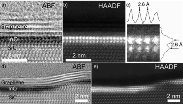
hydrogen intercalation of graphene and associated regular termination of Si dangling bonds by hydrogen atoms; such enclosed space of surfaces of reduced energy can support formation of structures with atom-size thickness. Intercalated layers of In atoms at the graphene/SiC inter- face giving origin to 2D InO were recorded by parallel acquisition of annular bright-field (ABF) and high-angle annular dark field (HAADF) STEM images in combination with electron energy loss spectroscopy (EELS) spectrum imaging (SI). In Fig. 1 (a-b), ABF- and HAADF-STEM images of the intercalated layer are shown at atomic resolution, where the 2D structure extends from Fig. 1 (a) into Fig. 1 (b) such that half of the imaged area is shown by ABF-, while the other is shown by HAADF- STEM. The SiC substrate appears at the bottom (zig-zag appearance) with two atomic layers of In, seen as dark dots in Fig. 1 (a) and bright dots in Fig. 1 (b). The atomic arrangement of the intercalated In atoms in this projection is perfectly square so that the out-of-plane and in-plane columnar distances are both 2.6 ± 0.1 Å, calibrated against the 4H- SiC lattice (c-axis), as shown in the line profiles in Fig. 1 (c). Above the intercalated layers of In, four layers of graphene are visible, partic- ularly in Fig. 1 (a), and partly in Fig. 1 (b). The amorphous and finally crystalline layer above the graphene is aluminum (Al), which was deposited to preserve the surface structure during FIB sample prepara- tion. In Fig. 1(d) and (e), the ABF- and HAADF-STEM images from a step on the SiC substrate are shown. The 2D InO extends along SiC steps on the surface, while in contrast graphene grows across the steps. It can be observed that accumulation of few layers may occur locally in the vi- cinity of a step.
EELS was applied for the investigation of the elemental composition across the interface and indicative of the availability of In-O bonding in the intercalated structure. Fig. 2 shows the core-loss EELS spectra including the C-K, In-M, O-K, Al-K and Si-K edges in the range from 250 to 2000 eV. The structure was sensitive to the applied beam current;
therefore, a spectrum image (SI) with reduced spatial resolution was recorded. The SI was recorded across the interface and laterally aver- aged to increase the signal to noise ratio of the spectra shown in Fig. 2.
Consequently, Fig. 2 can be viewed as a line scan across the interface with nm resolution. In the SiC at the bottom of Fig. 2, only C and Si are visible from their K-edges with onset at ~ 280 and ~ 1840 eV energy loss, as indicated in the graph. At the interface, seen already in spectrum (5), both In and O appears as seen from their M and K edges, at ~ 440 and ~ 530 eV energy loss, respectively. The In-M can be observed in (5) as a change of the background slope but it is most apparent in (6) together with O. Note also the apparent change in character of the C-K fine structure in (6) as the C bond is changed from sp3 to sp2 type from SiC to graphene, respectively. This spectrum is integrated across both the In and graphene layers and indicates that In bonds with O and hence forms a 2D InO structure. In (7) and above, C is only present as residual contamination, and the spectra has been background-subtracted after the C-edge for display purposes. From (7) and above, Al-K is present with the edge onset at ~ 1560 eV energy loss, together with O that is clearly being reduced in contrast to Al which is increasing. Apparently, the protective structure observed immediately above the graphene is amorphous AlOx.
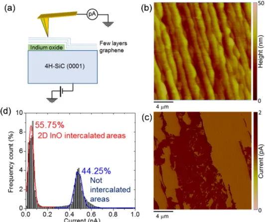
Nanoscale resolution current mapping by conductive atomic force microscopy (C-AFM) [23] was employed to evaluate the lateral unifor- mity of intercalated 2D InO, as well as to get insight in the electronic properties of the graphene/2D InO/SiC heterostructure. The experi- mental setup for C-AFM measurements is schematically illustrated in Fig. 3 (a). A Pt-coated tip is scanned on the surface while a bias is applied to the sample backside, and the current flowing vertically across the heterostructure is collected by a current sensor with pA sensitivity connected to the tip. Fig. 3 (b-c) shows a representative morphology image and the corresponding current map acquired on a large area (20 µm ×20 µm) by applying a tip-to-sample potential difference of 1 V. The stepped morphology in Fig. 3 (b) originates from the step-bunching of SiC during high temperature growth of epitaxial graphene. The current map in Fig. 3 (c) clearly shows distinct areas with lower and higher
injected current, which were associated to the 2D InO-intercalated and not-intercalated epitaxial graphene regions, respectively. The histogram of current values extracted from this map is reported in Fig. 3 (d), from which the percentages of InO -intercalated (~55.75%) and not inter- calated (44.25%) graphene was estimated.
A higher resolution current map collected at the boundary between the intercalated and not-intercalated InO regions is reported in Fig. 4 (a).
A line-scan extracted along the dashed red line in the current map is reported in Fig. 4 (b), showing a reduction of the injected current by about a factor of six due to the presence of this ultrathin barrier layer.
Furthermore, two typical local current–voltage characteristics, measured with the tip on InO-intercalated and not-intercalated gra- phene are reported in Fig. 4 (c). Both curves exhibit a rectifying behavior in the considered bias range (from − 1.3 V to 1.3 V), with the forward current onset at larger bias in the case of InO-intercalated graphene/SiC.
The two forward bias characteristics have been also reported on the
semi-log scale in the insert of Fig. 4 (c), to better highlight the differences.
This electrical behavior can be explained considering the schematic energy band diagrams for the graphene/SiC and graphene/InO/SiC heterojunctions depicted in Fig. 4 (d) and (e). Current injection across the quasi-free-standing graphene/SiC junction can be described by thermionic emission above the Schottky barrier, as recently discussed in Reference [24]. The black line in Fig. 4 (c) (insert) is the fit of the for- ward bias characteristics of this junction with the thermionic emission equation:
ITE=AtipA*T2exp(− qΦB,Gr
kBT )exp(qVtip
nkBT) (1)
where graphene/SiC Schottky barrier height value (ΦB,Gr =1.1 eV) and the ideality factor (n =1.5) are the fitting parameters, Atip=πr2tip is the tip contact area (with rtip =5 nm), A* =146 A cm−2 K−2 is the 4H- SiC Richardson constant, q is the electron charge, kB is the Boltzmann constant and T =300 K. On the other hand, for the graphene/InO/SiC heterostructure it is reasonable to assume the combination of thermionic emission with direct tunneling of electrons from the SiC conduction band edge across the ultrathin InO layer. The black line in Fig. 4 (c) (insert) is the fit of the forward bias characteristic for this heterojunction with the equation:
ITE+DT=ITE(Vtip)exp [
− 4π ̅̅̅̅̅̅̅̅̅̅̅̅̅̅̅̅̅̅̅
meffΦB,InO
√ d
h ]
(2) where ΦB,InO is the energy difference between the conduction band minimum of InO and the conduction band edge of 4H-SiC, meff is the InO effective mass, h is the Planck’s constant, and d =0.52 nm is the InO bilayer thickness as evaluated by atomic resolution STEM analyses.
Assuming in the first approximation the same effective mass as in bulk In2O3
(meff =0.35me
)[25], a value of ΦB,InO=0.3eV was estimated by the fit of the I-Vtip curve with Eq (2). Hence, the conduction band minimum of 2D InO lies ~ 0.3 eV above that of 4H-SiC, resulting in an electron affinity value χInO≈2.8 eV for the intercalated InO layer (evaluated considering the typical electron affinity of ~ 3.1 eV for 4H- SiC). Noteworthy, χInO is significantly lower than the reported electron affinity (~ 4.2 eV) for crystalline bulk In2O3 [26]. It can be argued that this reduced electron affinity corresponds to a wider energy bandgap of the 2D InO, that we estimate to be in the order of 4.1 ± 0.1 eV, as Fig. 1.(a) ABF-STEM and (b) HAADF-STEM image showing 2D InO intercalated at graphene/SiC interface. (c) Projected line profiles of a magnified part of (b). The InO layer at a SiC step is shown in (d) and (e).
Fig. 2. EELS spectrum imaging results revealing the depth distribution of ele- ments across the interface; the averaged spectra are presented as a line profile showing energy losses in the range from 250 to 2000 eV.
compared to the literature value of 2.7 ±0.1 eV for 3D In2O3 [26]. The very different conduction band misalignment for the 2D InO indicates the occurrence of significant quantum confinement effects, also observed for other 2D materials with respect to 3D crystals [16]. The estimated wide bandgap energy value of 4.1 ±0.1 eV by C-AFM for the 2D InO agrees with the value of 4.11 eV obtained by first principles calculations at the HSE06 level of theory [18].
While there is an apparent intercalation of In atoms at the graphene/
SiC interface, the MOCVD process involves the strongly bonded (CH3)3In
precursor, which interacts with graphene. The (CH3)3In precursor holds common structural characteristics with other typical precursor imple- mented in MOCVD processes such as trimethylaluminum, (CH3)3Al [27]. Features of the stability of these two precursors are presented in Fig. 5.
Noteworthy, ab initio molecular dynamics simulations have provided understanding of atomistic and electronic processes for formation of aluminum (Al) adatoms on graphene consequent to (CH3)3Al/graphene surface reactions [28]. Furthermore, formation of precursor-derived Fig. 3.(a) Schematic illustration of the C-AFM setup, (b) Morphology and (c) current map acquired with a tip-sample bias Vtip =1 V on large area (20 µm ×20 µm) to probe the uniformity of 2D InO intercalation. (d) Histogram of the current distribution extracted from the C-AFM map and percentage of 2D InO interca- lated graphene.
Fig. 4. (a) High resolution current map measured with a tip-sample bias Vtip =1 V and (b) current intensity line-scan in a region including InO- intercalated and not-intercalated graphene. (c) Representative current–voltage (I-Vtip) charac- teristics collected with the C-AFM tip on the graphene/SiC (red) and graphene/InO/SiC (black) regions. The insert shows a semi log plot of the two I-Vtip curves under forward bias po- larization and the fit with the thermionic emis- sion (TE) and with the combined thermionic emission and direct tunnelling (TE +DT) models.
Energy band diagrams for the (d) graphene/SiC and (e) graphene/InO/SiC heterojunctions.
carbon adatoms on graphene [28] has been associated with weakening of carbon bonds in the vicinity of pre-existing defects in graphene; thus, facilitating defects enlargement in the graphene bonding network and consequent atom intercalation [15]. Indium atoms are larger, heavier, and with wider electron shell than aluminum atoms. The dissociative patterns and atomistic pathways for the formation of In adatoms on graphene and their intercalation consequent to (CH3)3In/graphene surface reactions may differ from the case of the (CH3)3Al precursor.
Nevertheless, the reasoning that reflects paths for dissociative adsorp- tion of strongly bonded metal organic precursors, formation of indi- vidual metal adatoms, and subsequent functionalization of graphene that opens channels for intercalation [28], can also apply to the case of the (CH3)3In precursor. The delivery of the (CH3)3Al or (CH3)3In pre- cursor can be followed by a delivery of ammonia precursor, NH3, in a discerned scheme, as in our previous experiments, which resulted in the formation of 2D AlN and 2D InN confined at the graphene/SiC interface [15,17]. In the absence or deficiency of NH3 delivery, oxygen atoms may outcompete nitrogen atoms and participate in the formation of bonds with indium atoms. Therefore, common trace H2O and O2 (<0.5 vol ppm) in the gas stream may prove an effective source of oxygen for formation of 2D InO at the atom-size-scale. Oxygen species are inevi- tably present in MOCVD environment and In is known to be selective to the formation of indium oxide [29].
Noticeably, 2D InN and 2D InO manifest themselves in two different structural configurations, as predicted by first-principles calculations, reflected in our experiments, and consequently giving motivation for their respective assignment. The experimentally obtained structure of 2D InN [17] is underlined by the stacking pattern of two monolayers in their most stable configuration in agreement with predictive modeling results [11]. 2D InO, by comparison, is underlined by a different hex- agonal structure [18]: two sub-layers of In atoms form the skeleton of the 2D InO monolayer, which consists in its entirety in four atomic sub- layers in the sequence of O-In–In-O, and the In atoms are in “atop” po- sitions being clearly recognized in Fig. 2(b) and (c) in the experimentally obtained structure.
4. Conclusions
In summary, we report experimental evidence for the formation of 2D InO and its material and electrical characteristics. Targeted inter- calation of In atoms at the graphene/SiC interface was achieved through robust MOCVD processes. The intercalated layers of In atoms can give origin to a diversity of chemical and structural arrangement as directed by the deposition kinetics, which can drive transformations in the design and performance of 2D nanoelectronics devices.
CRediT authorship contribution statement
Anelia Kakanakova-Georgieva: Conceptualization, Investigation, Writing - original draft, Writing - review & editing, Project adminis- tration, Funding acquisition. Filippo Giannazzo: Investigation, Re- sources, Writing - original draft, Writing - review & editing. Giuseppe Nicotra: Investigation. Ildik´o Cora: Investigation. Gueorgui K.
Gueorguiev: Investigation, Writing - review & editing. Per O.Å. Pers- son: Investigation, Resources, Writing - original draft, Writing - review
& editing. B´ela P´ecz: Investigation, Resources, Writing - review &
editing.
Declaration of Competing Interest
The authors declare that they have no known competing financial interests or personal relationships that could have appeared to influence the work reported in this paper.
Acknowledgements
The authors thank Dr. T. Iakimov and Prof. R. Yakimova for kindly providing samples of epitaxial graphene. This work was supported by FLAG-ERA 2015 JTC project GRIFONE through Swedish Research Council VR 2015-06816 (A. Kakanakova-Georgieva, project leader GRIFONE), National Research Development and Innovation Office, Hungary NN 118914 (B. P´ecz), and in-kind resources of CNR-IMM, Italy.
A. K.-G. and G. K. G. acknowledge support through project VR 2017- 04071. F. G. acknowledges support of the Italian Ministry of Educa- tion and Research (MIUR) under the project EleGaNTe (PON ARS01_01007). B. P. thanks the support of VEKOP-2.3.3-15-2016-00002 of the European Structural and Investment Funds. F. G. and B. P.
acknowledge the CNR-HAS 2019-2022 bilateral project GHOST II. P.O.
Å.P. acknowledges Swedish Foundation for Strategic Research (SSF) through the Research Infrastructure Fellow program no. RIF 14-0074, and the Knut and Alice Wallenberg’s Foundation for support of the electron microscopy laboratory in Link¨oping University.
References
[1] I.M. Watson, Metal organic vapour phase epitaxy of AlN, GaN, InN and their alloys:
A key chemical technology for advanced device applications, Coord. Chem. Rev.
257 (2013) 2120–2141.
[2] H. von Wenckstern, Group-III Sesquioxides: Growth, Physical Properties, and Devices, Adv. Electron. Mater. 3 (2017) 1600350.
[3] G. Shen, B. Liang, X. Wang, H. Huang, D. Chen, Z.L. Wang, Ultrathin In2O3 Nanowires with Diameters below 4 nm: Synthesis, Reversible Wettability Switching Behavior, and Transparent Thin-Film Transistor Applications, ACS Nano 5 (2011) 6148–6155.
[4] N.-J. Ku, C.-H. Wang, J.-H. Huang, H.-C. Fang, P.-C. Huang, C.-P. Liu, Energy Harvesting from the Obliquely Aligned InN Nanowire Array with a Surface Electron-Accumulation Layer, Adv. Mater. 25 (2013) 861–866.
[5] C.L. Freeman, F. Claeyssens, N.L. Allan, Graphitic Nanofilms as Precursors to Wurtzite Films: Theory, Phys. Rev. Lett. 96 (2006), 066102.
[6] H. S¸ahin, S. Cahangirov, M. Topsakal, E. Bekaroglu, E. Akturk, R.T. Senger, S. Ciraci, Monolayer honeycomb structures of group-IV elements and III-V binary compounds: First-principles calculations, Phys. Rev. B 80 (2009), 155453.
[7] D. Wu, M.G. Lagally, F. Liu, Stabilizing Graphitic Thin Films of Wurtzite Materials by Epitaxial Strain, Phys. Rev. Lett. 107 (2011), 236101.
[8] E.F. de Almeida Junior, F. de Brito Mota, C.M.C. de Castilho, A. Kakanakova- Georgieva, G.K. Gueorguiev, Defects in hexagonal-AlN sheets by first-principles calculations, Eur. Phys. J. B 85 (2012) 48.
[9] R.B. dos Santos, F. de Brito Mota, R. Rivelino, A. Kakanakova-Georgieva, G.
K. Gueorguiev, Van der Waals stacks of few-layer h-AlN with graphene: an ab initio study of structural, interaction and electronic properties, Nanotechnology 27 (2016), 145601.
[10] A. Onen, D. Kecik, E. Durgun, S. Ciraci, GaN: From three- to two-dimensional single-layer crystal and its multilayer van der Waals solids, Phys. Rev. B 93 (2016), 085431.
[11] V. Wang, Z.Q. Wu, Y. Kawazoe, W.T. Geng, Tunable Band Gaps of InxGa1−xN Alloys: From Bulk to Two-Dimensional Limit, J. Phys. Chem. C 122 (2018) 6930–6942.
[12] M. Stella Prete, O. Pulci, F. Bechstedt, Strong in- and out-of-plane excitons in two- dimensional InN nanosheets, Phys. Rev. B 98 (2018), 235431.
Fig. 5. Representation of optimized structures, including In-C and Al-C bond lengths, for precursors trimethylindium, (CH3)3In, and trimethylaluminum, (CH3)3Al, as per Reference [27]. Features of their stability are indicated by cohesive energy per atom, and Gibbs free energy of formation as per Refer- ence [27].
[13] P. Tsipas, S. Kassavetis, D. Tsoutsou, E. Xenogiannopoulou, E. Golias, S.A. Giamini, C. Grazianetti, D. Chiappe, A. Molle, M. Fanciulli, A. Dimoulas, Evidence for graphite-like hexagonal AlN nanosheets epitaxially grown on single crystal Ag (111), Appl. Phys. Lett. 103 (2013), 251605.
[14] V. Mansurov, T. Malin, Yu. Galitsyn, K. Zhuravlev, Graphene-like AlN layer formation on (111) Si surface by ammonia molecular beam epitaxy, J. Cryst.
Growth 428 (2015) 93–97.
[15] A. Kakanakova-Georgieva, G.K. Gueorguiev, D.G. Sangiovanni, N. Suwannaharn, I.
G. Ivanov, I. Cora, B. P´ecz, G. Nicotra, F. Giannazzo, Nanoscale phenomena ruling deposition and intercalation of AlN at the graphene/SiC interface, Nanoscale 12 (2020) 19470–19476.
[16] Z.Y. Al Balushi, K. Wang, R.K. Ghosh, R.A. Vil´a, S.M. Eichfeld, J.D. Caldwell, X. Qin, Y.-C. Lin, P.A. DeSario, G. Stone, S. Subramanian, D.F. Paul, R.M. Wallace, S. Datta, J.M. Redwing, J.A. Robinson, Two-dimensional gallium nitride realized via graphene encapsulation, Nat. Mater. 15 (2016) 1166–1171.
[17] B. P´ecz, G. Nicotra, F. Giannazzo, R. Yakimova, A. Koos, A. Kakanakova-Georgieva, Indium Nitride at the 2D Limit, Adv. Mater. 33 (2021) 202006660.
[18] Y. Guo, L. Ma, K. Mao, M. Ju, Y. Bai, J. Zhao, X.C. Zeng, Eighteen functional monolayer metal oxides: wide bandgap semiconductors with superior oxidation resistance and ultrahigh carrier mobility, Nanoscale Horiz. 4 (2019) 592–600.
[19] D. Nilsson, E. Janz´en, A. Kakanakova-Georgieva, Strain and morphology compliance during the intentional doping of high-Al-content AlGaN layers, Appl.
Phys. Lett. 105 (2014), 082106.
[20] M. Feneberg, N.T. Son, A. Kakanakova-Georgieva, Exciton luminescence in AlN triggered by hydrogen and thermal annealing, Appl. Phys. Lett. 106 (2015), 242101.
[21] R. Yakimova, Ch. Virojanadara, D. Gogova, M. Syv¨aj¨arvi, D. Siche, K. Larsson, L. Johansson, Analysis of the Formation Conditions for Large Area Epitaxial Graphene on SiC Substrates, Mater. Sci. Forum 645–648 (2010) 565–568.
[22] I. Shtepliuk, I.G. Ivanov, T. Iakimov, R. Yakimova, A. Kakanakova-Georgieva, P. Fiorenza, F. Giannazzo, Raman probing of hydrogen-intercalated graphene on Si-face 4H-SiC, Mater. Sci. Semicond. Process. 96 (2019) 145–152.
[23] F. Giannazzo, G. Greco, F. Roccaforte, C. Mahata, M. Lanza, in Electrical Atomic Force Microscopy for Nanoelectronics (Ed: U. Celano), Springer Nature, Cham, Switzerland, 2019, Ch. 10.
[24] F. Giannazzo, I. Shtepliuk, I.G. Ivanov, T. Iakimov, A. Kakanakova-Georgieva, E. Schiliro, P. Fiorenza, R. Yakimova, Probing the uniformity of hydrogen ` intercalation in quasi-free-standing epitaxial graphene on SiC by micro-Raman mapping and conductive atomic force microscopy, Nanotechnology 30 (2019), 284003.
[25] D.R. Hagleitner, M. Menhart, P. Jacobson, S. Blomberg, K. Schulte, E. Lundgren, M. Kubicek, J. Fleig, F. Kubel, C. Puls, A. Limbeck, H. Hutter, L.A. Boatner, M. Schmid, U. Diebold, Bulk and surface characterization of In2O3(001) single crystals, Phys. Rev. B 85 (2012), 115441.
[26] M. Nazarzadehmoafi, S. Machulik, F. Neske, V. Scherer, C. Janowitz, Z. Galazka, M. Mulazzi, R. Manzke, Schottky contact by Ag on In2O3 (111) single crystals, Appl. Phys. Lett. 105 (2014), 162104.
[27] R. B. dos Santos, R. Rivelino, F. de Brito Mota, A. Kakanakova-Georgieva, G. K.
Gueorguiev, Feasibility of novel (H3C)nX(SiH3)3− n compounds (X =B, Al, Ga, In): structure, stability, reactivity, and Raman characterization from ab initio calculations, Dalton Trans. 44 (2015) 3356-3366.
[28] D.G. Sangiovanni, G.K. Gueorguiev, A. Kakanakova-Gueorguieva, Ab initio molecular dynamics of atomic-scale surface reactions: insights into metal organic chemical vapor deposition of AlN on graphene, Phys. Chem. Chem. Phys. 20 (2018) 17751–17761.
[29] H.F. Liu, N.L. Yakovlev, D.Z. Chi, W. Liu, Post-growth thermal oxidation of wurtzite InN thin films into body-center cubic In2O3 for chemical/gas sensing applications, J. Solid State Chem. 214 (2014) 91–95.
![Fig. 5. Representation of optimized structures, including In-C and Al-C bond lengths, for precursors trimethylindium, (CH 3 ) 3 In, and trimethylaluminum, (CH 3 ) 3 Al, as per Reference [27]](https://thumb-eu.123doks.com/thumbv2/9dokorg/753980.32153/5.892.65.425.85.248/representation-optimized-structures-including-precursors-trimethylindium-trimethylaluminum-reference.webp)
