1
Spontaneous doping of 2D MoS
2basal plane by oxygen substitution during ambient exposure
János Pető1, Tamás Ollár2,Péter Vancsó1,3, Zakhar I. Popov4, Gábor Zsolt Magda1, Gergely Dobrik1, Chanyong Hwang5, Pavel B. Sorokin4, and Levente Tapasztó1*
1. Hungarian Academy of Sciences, Centre for Energy Research, Institute of Technical Physics and Materials Science, 2DNanoelectronics Lendület Research Group 1121 Budapest, Hungary
2. Hungarian Academy of Sciences, Centre for Energy Research, Institute for Energy Security and Environmental Safety, Surface Chemistry and Catalysis Department 1121 Budapest, Hungary
3. University of Namur, Department of Physics, 61 rue de Bruxelles, 5000 Namur, Belgium 4. National University of Science and Technology MISiS, 119049 Moscow, Russia
5. Korea Research Institute for Standards and Science, Daejeon 305340, South Korea
* tapaszto@mfa.kfki.hu
The chemistry of atomically thin crystals can markedly differ from the
conventional surface reactions of their bulk counterparts. Here we provide atomic level insights into the ambient oxidation reaction of MoS2 monolayers by scanning tunneling microscopy measurements. In contrast to the generally accepted view of
environmentally inert basal plane, we found that oxygen atoms spontaneously
incorporate into the basal plane of MoS2 single layers during ambient exposure. While the basal plane was found to be stable against commonly investigated O chemisorption and MoO3 conversion, an oxygen substitution reaction has been revealed, upon which individual sulfur atoms are one by one replaced by oxygen, giving rise to a novel 2D solid solution type MoS2-xOx crystal. This oxidation process enables the chemical modification of single atomic sites of 2D crystals opening new routes towards their efficient defect engineering. An eloquent example is that the O substitution sites present all over the basal plane substantially increase the catalytic activity of the 2D MoS2
crystals for electrochemical H2 evolution reaction.
2 Layered materials display thickness-dependent properties when approaching the single layer limit. Chemistry is no exception, as evidenced by the oxidation and hydrogenation of graphene1,2. Surface chemistry is a particularly promising approach for engineering the
properties of 2D materials, given their fully exposed atomic structure. However, the chemistry of 2D Transition Metal Dichalcogenide (TMDC) crystals is mainly defined by their edges3, where coordinatively unsaturated sites prevail. Not coincidentally, these reactive edge sites were also found to be responsible for the catalytic activity of MoS24,5, one of the most widely studied TMDC materials. However, the chemical modification restricted to edges is only efficient in nanoscale islands6, as the edge to surface ratio drastically decreases in the 2D limit. Consequently, for 2D crystals it is of particular importance to chemically and
catalytically activate their entire basal plane. Oxidation has widely been studied for graphene as a promising approach towards its efficient exfoliation7. For 2D TMDC crystals the
oxidation reaction is also of particular importance, as for some crystals it can spontaneously proceed under ambient conditions. Therefore, its study is essential for understanding their long-term environmental stability, as well as it can open new routes towards chemically engineering their properties.
While some TMDC crystals, such as HfSe2, MoTe2 or WTe2, are known to be air- sensitive8,9,10 as they rapidly degrade under ambient, the most widely investigated members of the TMDC family (MoS2, MoSe2, WS2, WSe2) have generally been considered air-stable11,12, based also on decades-long experience with their bulk crystals. Nevertheless, it has been demonstrated that in single layer form the oxidation of MoS2 and WS2 also occurs under ambient conditions13. The detailed investigations revealed that the oxidation induced etching originates from edges and grain boundaries and proceeds towards the interior of the flakes.
Due to the higher strength of the Mo-O bonds, as compared to Mo-S, the substitutional oxidation of the 2D MoS2 basal plane is in principle also thermodynamically favorable14,15.
3 However, while at under-coordinated atomic sites on edges and grain boundaries, such
oxidation is a fast, low-barrier process14,15, the oxidation of the defect-free basal plane has been predicted to face relatively high kinetic barriers of about 1.6 eV,16, rendering the basal plane environmentally stable. Although experiments often reveal significantly lower activation energy values for the MoS2 oxidation, such as 0.54 eV or 0.98 eV17,18, no direct evidence on the ambient oxidation of the pristine MoS2 basal plane has been reported so far.
We propose that this is mainly due to the inability of the employed structural characterization methods to resolve single-atom level structural changes. Harsh oxidation processes, such as oxygen plasma treatment, UV-ozone exposure, electrochemical exfoliation, or high
temperature (> 300°C) annealing are able to oxidize the basal plane of MoS2 crystals. Based primarily on XPS investigations it was shown that such processes can lead either to covalent oxygen bonding to the top sulfur atoms 14,19, or the formation of completely oxidized MoO3
areas20,21,22 that can subsequently volatilize, leading to etching. However, neither process is ideal for chemically tuning the properties of MoS2 sheets. While the formation of MoO3
destroys the original MoS2 crystal lattice, yielding an overall disordered and fragmented structure, the chemisorption of oxygen onto chalcogen atoms is predicted to have a relatively weak influence on band structureand properties14,16. It has also been shown that oxidation can both enhance and degrade the catalytic activity of MoS2, depending on the structural
details23,24, further emphasizing the importance of investigating and controlling the resulting oxidized structure. The possibility of a substitutional oxidation reaction of MoS2 has also been raised as being thermodynamically preferred to oxygen chemisorption15,25; however, no clear experimental evidence has been reported so far. The controlled substitutional oxidation of the MoS2 basal plane would be a highly desirable reaction that preserves the original MoS2
crystal structure, while in contrast to O chemisorption, it is also expected to substantially
4 influence the electronic band structure, enabling a more efficient engineering of its
electronic14,16 and optical26 properties.
Here we show that the basal plane of the MoS2 monolayers subjected to long-term ambient exposure spontaneously undergo such oxygen substitution reactions giving rise to a novel, highly crystalline two-dimensional molybdenum oxy-sulfide phase.
Results and discussion
Ambient oxidation of the basal plane revealed at single-atom level
We have prepared mechanically exfoliated MoS2 single layers on atomically flat Au (111) substrates using a slightly modified version of a recently developed exfoliation technique27 yielding single layers with lateral dimension of hundreds of microns (see SI section I. for details). Such large area samples are characterized by an extremely low edge to surface ratio, grain boundary concentration, as well as a much smaller concentration and variety of intrinsic point defects28, establishing them as an excellent model system for studying the intrinsic chemical properties of the pristine basal plane. The exfoliated MoS2
samples have been stored under ambient conditions (air, room temperature and ambient light) for periods of up to 1.5 years. We have employed STM measurements to follow the atomic level structural changes in the basal plane structure of 2D MoS2 crystals during long-term ambient exposure. So far mainly optical, scanning electron and atomic force microscopy measurements have been employed to monitor the structural changes induced by oxidation in MoS2 layers. However, the spatial resolution of these methods does not allow detecting single atom level modifications. Imaging the atomic-scale structure of the MoS2 basal plane is possible by high resolution scanning Transmission Electron Microscopy (TEM). However, detecting light atoms such as oxygen with TEM is challenging due to their low contrast and easy knock-out29,30. By contrast, STM measurements can detect the unaltered structure of such oxygen defects due to its atomic resolution capability and the low energy of the
5 tunneling electrons31. Due to the slow oxidation reaction, and the noninvasive nature of the measurements, the structure and number of oxidation induced defect sites did not change during the STM imaging, enabling us to acquire atomic resolution snapshots of the oxidation process.
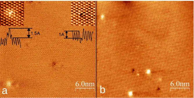
Atomic resolution STM images of the basal plane of a mechanically exfoliated MoS2
single layer after 1 month and 1 year of ambient exposure are shown in Fig. 1b and 1c, respectively. The STM images have been acquired on the same sample, but at different locations. In contrast to general expectations, STM measurements reveal clear modifications in the atomic structure of the MoS2 basal plane during ambient exposure. Freshly prepared 2D MoS2 crystals contain a native point defect density in the range of 1011 -1012 cm-2 (Fig. S2).
After a month of ambient exposure our STM measurements revealed the formation of new point defects all over the basal plane increasing their concentration into the 3×10¹² - 2×1013cm-2 range (Fig. 1b). The increase of the atomic scale defect concentration (up to 5×10¹³ - 1014 cm-2) appears more strikingly after a year exposure (Fig. 1c), when a substantial area of the sample surface is already covered by such defects, clearly evidencing the ability of the ambient exposure to create new defect sites in the basal plane structure of 2D MoS2
crystals. Although the defect density shows some spatial variation, as evidenced by the concentration ranges provided above, the effect of the ambient exposure time is more
significant. Higher resolution STM images (Fig. 1d) shed light on the atomic structure of the defects induced by ambient exposure. Dark triangles in the STM images of 2D MoS2 crystals are characteristic to sulfur atom vacancies 31. Within the dark triangles, bright spots can be clearly detected that have not been observed before. These central bright spots are a
pronounced feature of the experimental STM images, as their contrast is even stronger than that of S atoms of the MoS2 lattice. The most straightforward choice is to attribute the bright spots inside the S vacancies to atoms or molecules saturating the vacancies under ambient
6 conditions. Among ambient species oxygen has been predicted to be the energetically most favorable to saturate an S vacancy 14,16. To confirm this, we have performed detailed simulations of the STM images of various O-related defects in 2D MoS2 crystals based on DFT calculations of their electronic structure (Fig. S3). Our theoretical results reveal that the best agreement with the experimental STM data is provided by single oxygen atoms
substituting individual S atoms (saturating the S vacancy) displaying a dark triangle with a bright spot inside. Such a simulated STM image is shown in the inset of Fig.1d. We note that according to both calculations and measurements the contrast of the O substitutions is
dependent on the tip-sample distance; it only becomes fully apparent at small tip-sample distances (see SI section IV for details). While the agreement with experiments is far better than for any other calculated defect structure, it is not perfect. This can be attributed partly to the STM image distortions that are unavoidable at room temperature, and partly to the dark
‘halo’ often emerging near single atomic substitution sites in STM images32,33. The latter can be a signature of an electron depletion zone around a negatively charged defect site34. STM investigations cannot directly confirm the chemical identity of the incorporated atoms, XPS measurements are usually employed for such purposes. However, due to their low spatial resolution, it was not possible to selectively measure the single layer areas, as exfoliated samples are not homogenously covering the substrate. Furthermore, the relatively low concentration of the incorporated oxygen atoms (< 3 at%) makes such investigations challenging13. To gain more information on the nature of the defects progressively forming under ambient conditions, we have also performed Raman spectroscopy (Fig S5) and photoluminescence (PL) measurements. For the PL measurements we have transferred the MoS2 single layers from Au (111) to SiO2/Si substrates. PL spectra on aged samples revealed a new peak at 1.75 eV that is not present in freshly exfoliated samples (see Fig S6). This peak can be clearly associated with vacancy type defect formation35,36. Moreover, it has been
7 shown that such peak does not emerge under ultra-high vacuum conditions; the charge
transfer induced by the saturation of vacancies with environmental species (oxygen, nitrogen) is necessary36. These findings further support our STM and simulation data on the formation of oxygen saturated S vacancies.
The above findings clearly challenge the generally accepted view of environmentally inert MoS2 basal plane, and evidence that the ambient oxidation of the basal plane
spontaneously proceeds through formation of S vacancies and their saturation by oxygen. This oxidation process preserves the original crystal lattice with Mo sites in the trigonal prismatic configuration, but coordinated by five sulfur and an oxygen atom. The oxidation speed of the MoS2 basal plane under ambient was found to be of order of 1 atom / minute / μm2. This ultra-slow oxidation reaction in principle enables an extremely precise control of oxygen concentration in the MoS2 lattice. The slow reaction speed is most likely responsible for stabilizing the oxy-sulfide phase against the otherwise favorable full conversion to MoO320.
Since the oxidation process is expected to be kinetically limited14,16, by increasing the temperature, the oxidation speed should also increase. We have subjected a freshly exfoliated MoS2 /Au (111) sample to air inside a furnace heated to 400 K for one week. Subsequent STM investigation revealed a similar defect formation as at room temperature, but the oxygen site concentration reached values of 8×10¹² - 3×10 13 cm-2 already after a week of exposure (see Fig. S7). This clearly indicates that the oxygen substitution process has been accelerated by increasing the temperature. Furthermore, this observation also excludes the possibility that the ambient oxidation occurs due to the accidental presence of some more reactive oxygen species (e.g., ozone, superoxide, singlet oxygen). Increasing the temperature form 21°C to 127°C is not expected to significantly increase the formation of such reactive species. The accelerated oxygen substitution process at higher temperatures also provides a more feasible route for the synthesis of oxy-sulfide crystals.
8 The substitutional oxidation of MoS2 basal plane yields a novel 2D MoS2-xOx solid solution crystal phase (Fig. 1a).The formation of MoS2-xOx solid solution phase has already been proposed for sputter deposited MoS2 films37,38 ,39. However, so far the structure of the synthesized molybdenum oxy-sulfide films was found to be amorphous or highly disordered with poor long-range crystalline order40,41. Here we provide clear evidence for the formation of a highly crystalline 2D molybdenum oxy-sulfide phase. This provides a novel strategy for synthesizing new materials through chemical transformation of 2D crystals that are difficult to synthesize by other methods.
The STM investigations of 2D MoSe2 crystals (prepared and aged under the very same condition as 2D MoS2 crystals) revealed a strikingly different behavior upon long-term
ambient exposure. Fig. 2 shows atomic resolution STM images of freshly exfoliated and 1 year old MoSe2 single layers. The basal plane of the 2D MoSe2 crystal does not show
significant changes even after year-long ambient exposure. Native defects (Se vacancies and chemisorbed adatoms – see the inset of Fig. 2a) are present with a relatively low (1011 -1012 cm-2) density, but their concentration is not increasing during ambient exposure.
The energetics and kinetics of oxygen substitution
Based on the existing literature, it is difficult to interpret the experimentally observed striking differences in the ambient oxidation behavior of 2D MoS2 and MoSe2 basal planes.
However, most theoretical works so far focused on the chemisorption mechanism. Indeed, our experimental results confirm that the pristine basal planes of both MoS2 and MoSe2 single layers are stable against chemisorption or MoO3 transformation. We found that oxygen
substitution proceeds in the case of MoS2, but not for MoSe2. In contrast to chemisorption, the oxygen substitution mechanism implies the removal of S (Se) atoms during the oxidation process. To investigate the thermodynamics of this process, we have performed DFT calculations (see Methods for details) regarding the removal of S (Se) atoms from the basal
9 plane of the 2D MoS2 (MoSe2) crystals through oxidation. First, we have investigated the reaction of surface sulfur atoms of 2D MoS2 crystalswith oxygen, yielding volatile SO2
species and creating a sulfur vacancy in the MoS2 basal plane (Fig. 3a). The enthalpy of the reaction is calculated using the formula: ∆E = E (Reactants) – E (Products) = - 0.49 eV. Since the enthalpy of the final structures is lower than the initial, this implies that S atom removal by oxidation is thermodynamically favorable in the case of MoS2. By contrast, our DFT calculations show that the removal of a Se atom through oxidation of MoSe2 basal plane displays a positive oxidation enthalpy of ∆E = + 0.75 eV (Fig. 3b). This result evidences the thermodynamically unfavorable nature of selenium oxide formation, which hinders the formation of Se vacancies through oxidation and hence the substitutional oxidation of the MoSe2 basal plane, in agreement with the experimental observations.
Even though thermodynamically favorable, the substitutional oxidation of MoS2 basal plane is still expected to face kinetic barriers. To determine this we have performed detailed nudged elastic band (NEB) model calculations42 for determining the energy of transitional states and finding the potential barriers for the substitutional oxidation process. The results displayed in Fig 3c show that in the case of MoS2 the typical kinetic barrier height is about 1 eV for the proposed reaction pathway. We note that by considering the O saturation of the S vacancies the energy of the final state becomes by about - 4 eV lower (Fig S3), indicating the highly favorable nature of the O substitution process as a next step, in accordance with the experimental findings. By contrast, the barriers for the substitutional oxidation of MoSe2 basal plane are about 1.5 eV, with a thermodynamically unfavorable final state (Fig. 3d).
Consequently, both energetics and kinetics support our experimental findings on the differences between the oxidation of the 2D MoS2 and MoSe2 basal planes, reflecting the different oxidation mechanisms of sulfur and selenium based compounds. Furthermore, the kinetic barriers of about 1 eV height for the substitutional oxidation of MoS2 are predicted to
10 be surmounted at room temperature on month’s timescale, according to transition state
theory43.
Although the basal plane of the MoSe2 appears more stable, the overall environmental stability of the crystals is also dependent on their edge oxidation speed. We found that the oxidation proceeds much faster at the edges of MoSe2 single layers than on the MoS2 edges (Fig. S8, S9). Adsorbed contaminations are naturally present on both MoS2 and MoSe2
surfaces subjected to ambient. However, they role in the ambient oxidation process is expected to be more pronounced at edges and grain boundaries13,15, as they are known to preferentially attach to these high-energy sites instead of the pristine basal plane.
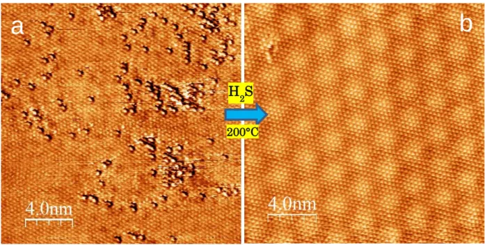
While structural disorder induced by invasive oxidation is unlikely to be fully reversible, the substitutional oxidation of the MoS2 basal plane does not damage the crystal lattice, so it can in principle be suitable for a fully reversible reduction. Indeed, we found that a simple annealing of the MoS2-xOx crystals in H2S atmosphere at 200°C for 30 minutes is able to fully restore the atomic structure of the pure 2D MoS2 phase. Two representative atomic resolution STM images of the MoS2 basal plane before and after the reduction (Fig. 4) clearly evidence that 2D MoS2-xOx solid solution crystals can be reduced to the pure, almost defect-free MoS2 phase. The feasibility of such a reduction process is also supported by our DFT calculations (Fig. S10). The atomically perfect reduction of the oxidized 2D MoS2-xOx
crystals enables a highly efficient engineering of their surface chemistry.
Catalytic activity of 2D MoS2-xOx crystals towards hydrogen evolution
To investigate how the oxygen substitution sites change the properties of MoS2 single layers, we have investigated the catalytic activity of 2D MoS2-xOx crystals for the
electrochemical hydrogen evolution reaction (HER) (see Methods for experimental details).
Polarization curve (I-E) measurements have been performed on both MoS2-xOx and MoS2
single layers. To make the comparison more direct and relevant, we have measured a 1 year
11 old MoS2-xOx flake before and after its reduction to the pure 2D MoS2 phase. This way, we could measure the catalytic activity of the very same flake both with and without O
substitution sites in the basal plane, as revealed by our STM characterization. The measured polarization curves and the corresponding Tafel plots shown in Fig.5 evidence a highly increased catalytic HER activity of the 2D MoS2-xOx solid solution crystals, as compared to the reduced pure 2D MoS2 phase. Consequently, this enhanced catalytic activity can be clearly related to the presence of substitutional O sites, the only structural feature that displays a correlation with ambient exposure time, according to atomic level structural STM data. We have also investigated the stability of the 2D MoS2-xOx crystals during 1000 catalytic cycles.
After an initial slight decrease by about 10%, the current density stabilizes, indicating a good long-term stability of the catalytic process (Fig. S11). Confocal Raman microscopy maps revealed that the 2D MoS2-xOx layer is still continuous after 1000 cycles and the measured Raman spectra remained practically unaltered (Fig. S12), while atomic resolution STM measurements confirmed that the O substitution sites are present after the catalytic process (Fig. S11).
A widely used parameter for predicting the catalytic activity of various sites is the hydrogen adsorption Gibbs free energy (ΔGH). We have calculated the ΔGH for O substitution sites and compared it to that of pristine MoS2 surface (see SI section X for calculation details).
We found that ΔGH is lowered to about half on the O sites (+ 1.2 eV) as compared to the S sites (+ 2.2 eV) of the basal plane, which means that hydrogen is much more likely absorbed on the O sites. However, even the substantially reduced ΔGH value of about 1 eV is still well above zero, indicating a not very favorable H adsorption. Nevertheless, other effects - not captured by ΔGH – can also play an important role in the catalytic activity. Since O atoms have a similar electron configuration to S atoms, it is often assumed that the O substitutions are fully passivating the S vacancies without significantly altering the electronic structure.
12 While O substitutions indeed remove the midgap states characteristic to sulfur vacancies44, they still substantially change the orbital composition of the valence and conduction bands (see SI section XI), as well as the electron affinity at the substitution sites. The
electronegativity and electron affinity of the dopants (including O substitutions) has been shown to play an important role in defining the catalytic activity of graphene45,46. To evaluate this effect for the O substitution sites of 2D MoS2 crystals, we have performed the Bader charge analysis (see SI section XII for details) that has proven useful for understanding the catalytic activity of sites where charge transfer plays an important role47. The Bader analysis evidenced a strong acceptor type behavior of the O substitution sites, characterized by almost two-times higher electron affinity (- 0.88 e-) as compared to S atoms (- 0.47 e-). The locally increased electron affinity combined with the experimentally measured overall n-doping of the MoS2 crystals (Fig S15) can give rise to localized negative charges on the O substitution sites. These partially screened negative charges can substantially facilitate the adsorption of positively charged H species from the acidic electrolyte. The effect of such charged dopants is not included in the ΔGH calculations, as it is challenging to treat charged impurities at the DFT level48. Therefore, we propose that the combined effects of the substantially decreased ΔGH and increased electronegativity at the O sites - both facilitating the absorption of H species - can give rise to the increased catalytic activity observed in 2D MoS2-xOx crystals.
Understanding the catalytic process is a highly challenging task, in big part due to the complexity of the experimentally investigated systems in strong contrast with the idealized theoretical models49. 2D MoS2-xOx provides an ideal model system for understanding the atomic level relations between active sites and catalytic HER activity, as it is characterized by a single type of active site, with experimentally known atomic structure, while edges and previously investigated more disordered MoS2 structures can host a variety of active sites with complex atomic configurations and often little experimental insight into their precise atomic
13 nature. These findings clearly evidence that the substitutional oxidation process of the MoS2
basal plane reported here can open new routes for engineering 2D electrocatalysts with single oxygen atom active sites of a much higher site density than previously achieved for individual hetero-atom catalysts50.
Methods
Sample preparation. The investigated MoS2 (and MoSe2) single layers have been prepared by mechanical exfoliation of bulk MoS2 (MoSe2) synthetic crystals of high structural quality (2DSemiconductors). We have employed a slightly modified version (see SI section I) of the mechanical exfoliation technique developed by us and discussed in details in ref. (27), providing single layer TMDC flakes with hundreds of microns lateral dimensions on
atomically flat Au (111) surfaces. The single layer nature of the investigated MoS2 and MoSe2
crystals has also been confirmed by Raman spectroscopy. The samples have been stored under ambient laboratory conditions: in air, at room temperature and ambient light conditions.
Characterization. Atomic resolution STM measurements have been performed on a Nanoscope E STM operating under ambient conditions. Tunneling spectroscopy data have been performed in an RHK PanScan STM under UHV conditions at room temperature. Large area flakes could be easily identified under an optical microscope enabling the guided landing of the STM tip on MoS2 single layers. Atomic resolution imaging could be achieved under ambient conditions with typical parameter ranges of |U bias| = 5 - 50 mV, and Itunnel = 1 - 3 nA.
Although the resolution of the hexagonal lattice of the top layer of S atoms can be routinely achieved, atomic resolution of individual point defects is challenging. Defects were clearly resolved when imaging at bias voltages (energies) within the band gap. This is possible due to the influence of the Au(111) substrate, which induce a small but finite density of states within the band gap (confirmed by our tunneling spectroscopy measurements), conferring a weak metallic character to the supported MoS2 single layers. Raman measurements have been
14 conducted on a confocal Raman microscope (Witec 300RSA) with 𝛌 = 532 nm and W = 1mW. We have ensured that during the Raman measurement the spectra of the sample did not change detectably.
Electrochemical measurements. The measurements have been conducted on selected sample areas (0.4 – 0.8 mm diameter) of a single 2D MoS2 flake supported by a 100 nm thick
Au(111) film on a glass substrate. Control measurements on the same Au (111) substrate as well as a Pt plate have been conducted in the same experimental configuration. To compare the performance of different samples in HER, linear sweep voltammetry was performed in a three-electrode configuration using 0.5M sulfuric acid electrolyte at room temperature. Silver / silver chloride and Pt wire were used as counter and reference electrodes, respectively.
Potential sweeps were acquired at a scan rate of 2 mV/s using a Bio-Logic SP-150 potentiostat.
Computational details. All calculations were performed on TMDC single layers in the framework of spin-polarized DFT theory implemented in the VASP software package, using the plane wave basis set and projector augmented wave method. Exchange-correlation effects were taken into account in the framework of local density approximation (LDA) and
generalized gradient approximation (GGA) by Perdew–Burke–Ernzerhof (PBE) functional.
The defects were modelled in periodically repeated 88 supercells. The Brillouin zone of the supercells was sampled with (2×2×1) Monkhorst−Pack mesh of k-points for geometry optimization and (441) for STM-image calculations. The cutoff energy for the plane-wave basis set was set to be 400 eV. To avoid artificial interactions between periodic replicas of low-dimensional nanoclusters, a vacuum interval of 15 Å was introduced in all supercell geometry. The nudged elastic band (NEB) method was applied for modeling transitional states and finding potential barriers of MoS2 and MoSe2 oxidation.
15
Figures
Figure 1. 2D MoS2-xOx solid solution crystals by ambient oxidation of MoS2. a) Schematic atomic structure of the MoS2-xOx solid solution monolayer. b)-d) Atomic resolution STM images (5mV, 2nA) of an exfoliated MoS2 single layer after one month (b) and one year (c) ambient exposure. d) Higher resolution STM image revealing the incorporation of the oxygen (bright spots) into the S vacancies (dark triangles). Inset shows simulated STM image based on DFT calculations of an oxygen saturated S vacancy site in the 2D MoS2 crystal.
a b
c d
16
Figure 2. Ambient stability of 2D MoSe2 basal plane. Atomic resolution STM images (5mV, 1nA) of 2D MoSe2 crystals on Au (111) substrate freshly prepared (a) and after 1 year of ambient exposure (b), revealing a remarkable ambient stability of the basal plane. The insets of panel (a) show higher resolution STM images and the corresponding line cuts of bright (chemisorbed adatom) and dark (Se vacancy) defect sites.
a b
17 Figure 3. Energetics and kinetics of the oxygen substitution in the MoS2 and MoSe2 basal plane. Vacancy formation through oxidation displays a negative oxidation enthalpy for 2D MoS2 (a) while it is positive for MoSe2, protected from oxidation by the endothermic nature of SeO2 formation(b). Kinetic energy barriers calculated by the nudged elastic band model for 2D MoS2 (c) and 2D MoSe2 (d) crystals.
a b
c d
18
Figure 4. Reduction of 2D MoS2-xOx to perfect MoS2. Representative atomic resolution STM images (5mV, 2nA) of 2D MoS2-xOx before (a) and after (b) 30 minutes annealing at 200° C in H2S atmosphere, evidencing the atomically perfect reduction of the oxy-sulfide solid solution to the pure MoS2 phase.
b
H2S.
200°C 30min
a b
19 Figure 5. Catalytic activity of 2D MoS2-xOx for hydrogen evolution. Linear sweep
votammogram curves (a) and the corresponding Tafel plots (b) for: Au substrate, MoS2 single layer, MoS2-xOx single layer (1 year old), and Pt substrate, revealing a significantly higher catalytic activity of the 2D oxy-sulfide phase as compared to the pure MoS2 phase, attributed to the novel catalytically active O substitution sites emerging on the basal plane during the substitutional oxidation process.
a b
20
References
1 Liu, L. et al. Graphene oxidation: thickness-dependent etching and strong chemical doping.
Nano Lett. 8, 1965-1970 (2008)
2 Luo, Z. et al. Thickness-dependent reversible hydrogenation of graphene layers. ACS Nano 3, 1781-1788 (2009)
3 Chhowalla, M. et al. The chemistry of two-dimensional layered transition metal dichalcogenide nanosheets. Nat. Chem. 5, 263-275 (2013)
4. Jaramillo, T.F. et al. Identification of active edge sites for electrochemical H2 evolution from MoS2 nanocatalysts. Science 317, 100-102 (2007)
5. Lauritsen, J.V. et al. Hydrodesulfurization reaction pathways on MoS2 nanoclusters revealed by scanning tunneling microscopy. J. Catal. 224, 94-160 (2004)
6 Lauritsen, J.V. et al Size-dependent structure of MoS2 nanocrystals. Nature Nanotechnol. 2, 53-58 (2007)
7 Dreyer, D.R., Park, S., Bielawski, C.W. & Ruoff, R.S. The chemistry of graphene oxide.
Chem. Soc. Rev. 39, 228-240 (2010)
8 Mirabelli, G. et al. Air sensitivity of MoS2, MoSe2, MoTe2, HfS2, HfSe2. J Appl Phys 120, 125102 (2016)
9 Yue, R. et al. HfSe2 films: 2D transition metal dichalcogenides grown by molecular beam epitaxy. ACS Nano 9, 474-480 (2015)
10 Lee, C.H. et al. Tungsten ditelluride: a layered semimetal. Sci. Rep. 5, 10013 (2015) 11 Li, Y., Zhou, Z., Zhang, S. & Chen, Z. MoS2 nanoribbons: high stability and unusual
electronic and magnetic properties. J. Am. Chem. Soc. 130, 16739−16744 (2008).
12 Grønborg, S.S. et al. Synthesis of Epitaxial Single-Layer MoS2 on Au(111). Langmuir 31, 9700−9706 (2015).
21 13. Gao, J., Li, B., Tan, J., Chow, P., Lu, T.-M. & Koratkar, N. Aging of Transition Metal
Dichalcogenide Monolayers, ACS Nano 10, 2628−2635 (2016).
14. Longo, R.C. et al., Intrinsic air stability mechanisms of two-dimensional transition metal dichalcogenide surfaces: basal plane versus edge oxidation. 2D Mater. 4, 025050 (2017) 15 Martincova, J., Otyepka, M. & Lazar, P. Is single layer MoS2 stable in the air? Chem. Eur.
J. 23, 13233-39 (2017)
16 Santosh, K.C., Longo, R.C, Wallace, R. M. & Cho, K. Surface oxidation energetics and kinetics on MoS2 monolayer, J. Appl. Phys. 117, 135301 (2015).
17 Rao, R., Islam, A.E., Campbell, P.E., Vogel, E.M. & Marujama, B. In situ thermal oxidation kinetics in few layer MoS2. 2D Mater. 4, 025058 (2017)
18 Bonde, J., Moses, P.G., Jaramillo, T.F., Norskov, J.K., Chorkendorff, I. Hydrogen evolution on nano-particulate transition metal sulfides. Faraday Discuss. 140, 219-223 (2009)
19. Angelica, A. et al., HfO2 on UV-O3 exposed transition metal dichalcogenides: interfacial reactions study. 2D Mater. 2, 014004 (2015)
20 Walter, T.N, Kwok, F., Simchi, H., Aldosari, H.M. & Mohney, S.E. Oxidation and oxidative vapor-phase etching of few-layer MoS2. J. Vac. Sci. Technol. 35, 021203 (2017)
21. Jaehyun, J. et al. Improved growth behavior of atomic-layer-deposited high-k dielectrics on multilayer MoS2 by oxygen plasma pretreatment. ACS Appl. Mater. Inter. 5, 4739-4744 (2013)
22. Pingli, Q. et al., In situ growth of double-layer MoO3/MoS2 film from MoS2 for hole- transport layers in organic solar cell. J. Mater. Chem. A 2, 2742-2756 (2014).
23 Voiry, D., et al, Conducting MoS2 nanosheets as catalysts for hydrogen evolution reaction.
Nano Lett. 13, 6222, (2013)
24 Juanfeng, X. et al. Controllable disorder engineering in oxygen-incorporated MoS2 ultrathin nanosheets for efficient hydrogen evolution. J. Amer Chem. Soc. 135, 17881-17888 (2013).
22 25 Liu, X. et al. Insight into the structure and energy of Mo27SxOy clusters. RSC Advances 7,
9513-9520 (2017)
26 Shu, H., Li, Y., Niu, X. & Wang, J. Greatly enhanced optical absorption of a defective MoS2
monolayer through oxygen passivation. ACS Appl. Mater. Interfaces 8, 13150-56 (2016) 27. Magda, G.Z., Pető, J., Dobrik, G., Hwang, C., Biró, L.P. & Tapasztó, L. Exfoliation of
large-area transition metal chalcogenide single layers. Sci Rep. 5, 14714 (2015)
28. Jinhua, H. et al., Exploring atomic defects in molybdenum disulphide monolayers, Nat.
Comm. 6, 6293 (2015).
29 Krivanek O.L. et al. Atom-by-atom structural and chemical analysis by annular dark field electron microcopy. Nature 464, 571 (2010)
30Komsa, H.P. et al., Two-Dimensional Transition Metal Dichalcogenides under Electron Irradiation: Defect Production and Doping. Phys. Rev. Lett. 109, 035503 (2012).
31 Vancsó, P. et al., The intrinsic defect structure of exfoliated MoS2 single layers revealed by Scanning Tunneling Microscopy. Sci. Rep. 6, 29726 (2016).
32 Nagl, C., Haller, O., Platzgummer, E., Scmid, M. & Varga, P. Submonolayer growth of Pb on Cu (111) : surface alloying and de-alloying. Surf. Sci. 321, 237-248 (1994)
33 Li, Z. et al. Spontaneous doping of two-dimensional NaCl films with Cr atoms: aggregation and electronic structure. Nanocale 7, 2366 (2015)
34 Bampoulis, P. et al. Defect dominated charge transport and Fermi level pinning in MoS2/metal contacts. ACS. Appl. Mater. Interfaces 9, 19278-86 (2017)
35 Chow, P.K., et al. Defect induced photoluminescence in monolayer semiconducting transition metal dichalcogenides. ACS Nano 9, 1520-1527 (2015)
36 Tongay, S., et al. Defects activated photoluminescence in two-dimensional semiconductors:
interplay between bound, charged and free excitons. Sci. Rep. 3, 2657 (2013)
23 37 Lince, J.R. Mo2-xOx solid solutions in thin films produced by RF-sputter-deposition, J.
Mater. Res. 5, 218 (1990).
38 Lince, J. R., Hilton, M.R. & Bommannavar, A.S. Oxygen substitution in sputter deposited MoS2 films studied by extended X-ray absorption fine-structure, X-ray photoelectron spectroscopy and X-ray diffraction. Surf. Coat. Technol. 43-44, 640 (1990).
39 Fleischauer, P.D. & Lince, J.R. A comparison of oxidation and oxygen substitution in MoS2 solid film lubricants. Tribol. Int. 32, 627-636 (1999).
40 Benoist, L., Gonbeau, D., Pfister-Guillouzo, G., Schmidt, E., Meunier, G. & Levasseur, A.
X-ray photoelectron spectroscopy characterization of amorphous molybdenum oxysulfide thin films. Thin Solid Films 258, 110-114 (1995).
41 Sung, H.S. et al. Bandgap widening of phase quilted, 2D MoS2 by oxidative intercalation.
Adv. Mater. 27, 3152-3158 (2015)
42 Henkelman, G., Uberuaga, B.P. & Jónsson, H. A climbing image nudged elastic band method for finding saddle points and minimum energy paths. J. Chem. Phys. 113, 9901–
9904 (2000)
43 Nan, H., et al. Strong Photoluminescence enhancement of MoS2 through defect engineering and oxygen bonding. ACS Nano 8, 5738-5745 (2014)
44 Hong, L. et al., Activating and optimizing MoS2 basal planes for hydrogen evolution through the formation of strained sulphur vacancies, Nat. Mater. 15, 48-53 (2016).
45 Xia, Z., Hydrogen evolution guiding principles, Nat. Energy 1, 16155 (2016)
46 Jiao, Y., Zheng, Y., Davey, K. & Qiao, S.Z. Activity origin and catalyst design principles for electrocatalytic hydrogen evolution on hetero-atom -doped graphene. Nat. Energy 1, 16130 (2016)
24 47 Yang, N., Zheng, X., Li, L., Li, J. & /wei, Z., Influence of phosphorus configuration on
electronic structure and oxygen reduction reactions of phosphorus-doped graphene. J.
Phys. Chem. C 121, 19321 (2017)
48 Komsa, H.P., Berseneva, N., Krashenninikov, A. & Nieminen, R.M. Charged point defects in the flatland: accurate formation energy calculations in two-dimensional materials. Phys.
Rev. X 4, 031044 (2014)
49. Su, Y., Gao, S., Lei, F. & Xie, Y. Atomically-thin two-dimensional sheets for understanding active sites in catalysis. Chem. Soc. Rev. 44, 623-636 (2015)
50. Qiao, B. et al., Single-atom catalysis of CO oxidation using Pt1/FeOx. Nat. Chem. 3, 634- 641 (2011)
Acknowledgements
Funding. The work has been performed in the framework of the NanoFab2D ERC Starting grant, the H2020 Graphene Core2 project no. 785219 and the Korea Hungary Joint Laboratory for Nanosciences. L.T. acknowledges OTKA grant K108753 and the “Lendület” Program. The work was also supported by the VEKOP-2.3.2-16-2016-00011grant supported by the European Structural and Investment Funds. Z.I.P. and P.B.S. gratefully acknowledge the financial support of the Ministry of Education and Science of the Russian Federation in the framework of Increase Competitiveness Program of NUST “MiSIS” (No. K2-2017-001). Z.I.P. and P.B.S.
are grateful to the supercomputer cluster "NUST-MiSIS" provided by the Materials Modelling and Development Laboratory (supported via the Grant from the Ministry of Education and Science of the Russian Federation No. 14.Y26.31.0005),to the Information Technology Centre of Novosibirsk State University for providing access to the cluster computational resources.
P.V. acknowledges the “Plateforme Technologique de Calcul Intensif (PTCI),” which was supported by the F.R.S.-FNRS under Convention No. 2.5020.11. P.B.S. acknowledges the financial support of the RFBR, according to the research project No. 16-32-60138 mol_а_dk.
We are grateful for Dr. J.S. Pap for useful discussions on electrochemistry.
Author contributions. L.T. conceived and designed the experiments. J.P. and G.Z.M. prepared the samples and performed the STM measurements. T.O. performed the chemical reduction and
25 electrocatalytic experiments. Z.I.P, P.V., and P.B.S. performed the theoretical calculations.
G.D. and G.Z.M. conducted the Raman and PL investigations. L.T., P.B.S. and C.H. supervised the project. L.T. wrote the paper. All authors discussed the results and commented on the manuscript.