semiconductor BiTeBr
M´aty´as Kocsis,1 Oleksandr Zheliuk,2 P´eter Makk,1 Endre T´ov´ari,1P´eter Kun,3Oleg Evgenevich Tereshchenko,4, 5, 6 Konstantin Aleksandrovich Kokh,4, 6, 7 Takashi Taniguchi,8 Kenji Watanabe,9 Justin Ye,2 and Szabolcs Csonka1
1Department of Physics, Budapest University of Technology and Economics and MTA-BME Lend¨ulet Nanoelectronics Research Group, Budafoki ´ut 8, 1111 Budapest, Hungary
2Zernike Institute for Advanced Materials, University of Groningen, Nijenborgh 4, 9747 AG Groningen, the Netherlands
3Institute of Technical Physics and Materials Science, MFA, Centre for Energy Research, Hungarian Academy of Sciences, P.O. Box 49, 1525 Budapest, Hungary
4St. Petersburg State University, 198504, St. Petersburg, Russia.
5A.V. Rzhanov Institute of Semiconductor Physics, 630090, Novosibirsk, Russia.
6Novosibirsk State University, 630090, Novosibirsk, Russia.
7V. S. Sobolev Institute of Geology and Mineralogy, 630090, Novosibirsk, Russia.
8International Center for Materials Nanoarchitectonics,
National Institute for Materials Science, 1-1 Namiki, Tsukuba 305-0044, Japan
9Research Center for Functional Materials, National Institute for Materials Science, 1-1 Namiki, Tsukuba 305-0044, Japan
Non-reciprocal transport, where the left to right flowing current differs from the right to left flowing one, is an unexpected phenomenon in bulk crystals. BiTeBr is a non-centrosymmetric material, with a giant Rashba spin-orbit coupling which presents this unusual effect when placed in an in-plane magnetic field. It has been shown that this effect depends strongly on the carrier density, however, in-situ tuning has not yet been demonstrated. We developed a method where thin BiTeBr flakes are gate tuned via ionic-liquid gating through a thin protective hBN layer. Tuning the carrier density allows a more than 400 % variation of the non-reciprocal response in our sample.
Our study demonstrates how a few-atomic-layer-thin van der Waals protection layer allows ionic gating of chemically sensitive, exotic nanocrystals.
I. INTRODUCTION
Tuning the carrier density of nanostructures is essen- tial for various applications and the exploration of exotic scientific phenomena. It lies in the heart of the operation of field effect transistors, it allows the implementation of electron optical elements in graphene,[1–4] and affects valley excitons in 2D materials,[5] spin relaxation,[6] or the exchange coupling in spintronic devices.[7] Tuning of the carrier density is typically achieved by gate elec- trodes, which are separated from the nanostructure by an insulating layer. Ionic-liquid (IL) gating presents a much more effective alternative, by inducing a layer of charged ions at the surface of the sample.[8–10] Large gating efficiency of IL enables e.g. two-dimensional Ising superconductivity in semiconductor MoS2[11–13] or pro- motes ferromagnetism in platinum.[14]
However, the applicability of IL gating is limited, as it could induce changes in some systems.[15, 16] In this Letter we show how IL gating combined with a van der Waals protective layer can be applied to chemically sensi- tive crystals. In particular, we will demonstrate how the exotic, non-reciprocal resistance of BiTeBr crystals can be boosted by IL gating. First a brief introduction to the non-reciprocal resistance of BiTeBr is given, followed by the description of devices making use of a few-atomic- layer-thin hBN protection layer, and IL gating experi- mental results showing that the non-reciprocal resistance can be tuned by over 400 %.
The study of nonreciprocal phenomena in noncen-
trosymmetric materials[17], such as BiTeBr, dates back decades. The first such effect to be observed was magneto-chiral dichroism (MChD)[18–20], in systems where both inversion and time-reversal symmetries are broken. Other effects where nonreciprocal re- sponses play a central role include nonreciprocal dynam- ics of magnons in chiral-structure compounds such as LiFe5O8[21] and Cu2OSeO3[22], and nonreciprocal trans- port phenomena,[23, 24] which is the focus of this work.
In crystals without inversion symmetry, such as BiTeBr[25–27], a very surprising non-reciprocity has been observed in the presence of an in-plane magnetic field (B)[23]: the resistance of the sample depends on the po- larity of the applied voltage, as illustrated in Fig. 1.a.
The source of the non-reciprocal behaviour lies in the crystal structure of BiTeBr,[17] shown in Fig. 1.b., be- longing to the P3m1 space group. The alternating lay- ers of (BiTe)+ and Br- break inversion symmetry and induce a large polarization (P),[27, 28] and lead to a so- called giant-Rashba spin-orbit interaction (SOI).[29] The Rashba energy (ER) and wavenumber offset (kR) are in- dicated on Fig. 1.c, their fraction yields αR = 2EkR
R =
2 eVA as the Rashba parameter,[30, 31] one of the largest in any bulk material.[29] The strong Rashba SOI causes a helical spin structure to develop,[29, 32, 33] as indicated by the arrows in Fig. 1.c and d. Applying an in-plane magnetic field breaks time-reversal symmetry, and dis- torts the dispersion relation of the conduction band, as shown in Fig. 1.d. The spins parallel to the magnetic field (red) are shifted to lower energies, while the anti-parallel
FIG. 1. a) Due to the lack of inversion symmetry of the crystal and the presence of an in-plane magnetic field, the current flowing through the sample depends on the polarity of the electric field applied.[17, 23] b) The crystal structure of BiTeBr (projected on the 001 and 1120 planes).[25–27] The dashed lines show the border of a possible unit cell. c)The band structure of BiTeBr assuming a two dimensional crystal, however the theoretical calculations concern both two and three dimensional cases.[23] d) The band structure in an in-plane magnetic field. The direction of the magnetic field By, electric field Ex, and polarization P are indicated. e) Fermi surfaces near the energy minimum of the antiparallel spins, and colormap of the reciprocal of the effective massm∗. The cross section of the dispersion relation is taken at the dashed line of panel d.
(blue) spins are shifted up.
The Fermi surface for zero in-plane electric fieldEdis- torted by the magnetic field B, is shown by the white dashed line in Fig. 1.e, while for a finite field (E or−E) perpendicular to B it shifts, as indicated by the blue and orange outlines. Due to asymmetry introduced by the magnetic field and SOI, the electrons’ effective mass (along the xdirection) on each surface is different. As a result, the magnitude of the resulting charge current (I) depends on the direction of E with respect to B.
Specifically, it depends on the vector product,[17] and the voltage-current characteristic takes the form
V =IR0(1 +γP·B×I), (1) where I and B are in-plane, P is the polarization of the crystal and is always out-of-plane, R0 is the resis- tance at B = 0, and γ measures the strength of the non-reciprocity. γ is related to the carrier densityn by γ∝n12,[23] enabling us to tune non-reciprocity by modi- fying the carrier density. We note that based on Equation (1), in this relationIis the absolute, not RMS amplitude of the AC current.
It is important to note that the Fermi surface on Fig. 1.d and e is chosen, so that the deformation due to the Rashba effect is clearly visible, but the actual Fermi surface is probably at higher energies, and is also influ- enced by termination dependent effects.[27, 30, 31]
While external gates have been used to induce Rashba SOI in different materials, we estiamte that the displace- ment field due to the polar crystal structure is orders of magnitude stronger than what the IL gate can generate.
II. HETEROSTRUCTURES
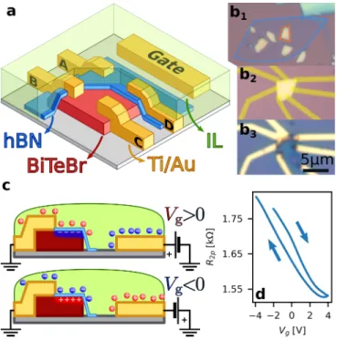
Due to the metallic nature and large carrier density of BiTeBr (3×1018cm−3 to 1.3×1019cm−3), we have chosen IL gating to control the carrier density. For ionic- liquid gating the sample and a separate gate electrode are covered by the IL, as shown in Fig. 2.a. A finite potential is applied to the gate electrode while the sample is grounded. This generates an accumulation of ions at the sample surface, as shown in Fig. 2.c. However, we found that BiTeBr is very sensitive to the ions of the IL, despite using DEME-TFSI as a gating medium, for its chemical stability. As soon as a nonzero voltage (Vg) was applied to the gate electrode, a current started to flow, and the BiTeBr flakes decomposed, as shown in Fig. 2.b.
To protect the BiTeBr flakes from the IL, we developed a heterostructure where the crystal is protected by a few atomic layer thin hBN flake, as shown in Fig. 2.a and b. The measurements presented here were carried out on the flake outlined in orange. As hBN is chemically stable, this technique can be used with a wide range of ILs, en-
FIG. 2. a)Schematic image of the sample, with the IL and hBN peeled away from the lower corner to show the BiTeBr flake. b)Optical images of the BiTeBr samples. b1The mea- sured sample, with the BiTeBr flake (orange outline) covered with hBN (blue outline). b2 An unprotected BiTeBr flake before liquid gating, with planned electrodes. b3 The above flake with contacts, destroyed by liquidgating. c)Schematic image of liquid gating. Due to the metallic nature of the sam- ple the bulk is screened, only a thin surface layer is affected by the gating. d) Two-point resistance as a function of the gate voltage at 220 K. The hysteretic behaviour is due to the slow motion of the ions.
abling previously incompatible materials to be used with liquid-gates. By distancing the ions from the surface the gating also becomes more homogeneous.[9]
We chose hBN flakes that were thin enough to allow for effective gating, but mechanically stable enough to cover the 40 nm to 50 nm thick BiTeBr flakes. For our purpose 3 nm to 5 nm thin flakes were selected.[34] Fig. 2.b shows an assembled stack, with the hBN flake outlined in blue and the measured BiTeBr flake in orange. BiTeBr flake composition was confirmed by Raman and EDS analysis, to sort out frequently occuring impurities, as discussed in Methods and the Appendix.
Ti/Au contacts were used to contact the BiTeBr flake.
Before evaporating the metallic contacts, the hBN under- neath was etched away. The same PMMA mask was used for the etching and the evaporation. This insures that the whole BiTeBr flake is covered either by the electrodes or hBN, and no ions can leak in at the hBN-electrode in- terface. Device fabrication is detailed inMethods. Pre- ceding the heterostructures showcased here, bare BiTeBr samples were fabricated and measured without IL gating as described in Appendix A.
The two-point resistance of BiTeBr as a function of the
FIG. 3. Second harmonic measurements before the IL gate is applied, showing the anti-symmetrized second-harmonic sig- nal. The relative orientation of the magnetic and electric field is shown in the insets. γ can be calculated from the slope of the second harmonic resistance using Equation (1). As ex- pected, no signal is detected in the parallel case.
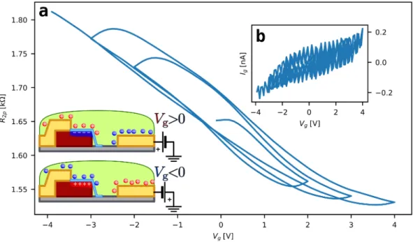
gate voltage (Vg) is shown in Fig. 2.d. The measurement was carried out at 220 K, above the glass transition tem- perature of DEME-TFSI. The change in the resistance shows that the gating is successful. The leakage current through the gate electrode was continuously monitored throughout the measurement, and never exceeded 0.3 nA as is shown in Fig. 6.b, confirming the isolation of BiTeBr from the IL by the hBN layer.
III. MEASURING THE NONRECIPROCITY Now we will turn to the measurement of the non- reciprocity. As shown in Equation (1), the non- reciprocity leads to the non-linear current voltage char- acteristics. This non-linearity can be easily observed by applying an AC current and measuring the sec- ond harmonic response. While other effects such as magnetoresistance,[17] or non-trivial thermoelectric behaviour[35] due to heating at the contacts, can gen- erate second harmonic signals of their own, all those scale with even powers of B, and can be avoided by taking only the antisymmetric part of the second har- monic resistance, ∆R2ω = 12 R2ω(B)−R2ω(−B)
=
1
2R0γB×I.[23]
The results of our initial measurements are plotted in Fig. 3, carried out before the IL was applied, at 2.5 K.
The insets show the orientations of the magnetic and
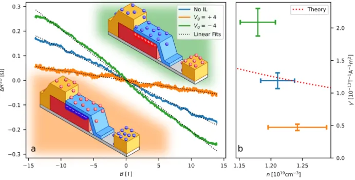
FIG. 4. a)The magnetic field dependence of the second-harmonic signal at different gate voltages. The insets demonstrate the position of the ions in the IL and the induced density changes in the BiTeBr in the different experiments. b)γ0 as a function of the carrier density extracted from Hall measurements. The dashed line shows theory from Ref. [23] without any fitting parameters. The divergence from theory can be explained by considering, that the second harmonic signal comes mainly from the gated surface layer, while the Hall measurements used for determiningnmeasure the whole crystal.
electric fields. ∆R2ω is measured as a function ofB, the value ofγis proportional to the slope.
To verify that the measured signal originates from the non-reciprocal resistance of BiTeBr and not some other effect, we took advantage of the relation from the first section, ∆R2ω ∝ B×I. As Fig. 3 demonstrates, the signal disappears when the fields are parallel (blue curve), indicating that the source of the signal is in- deed the non-reciprocal resistance of BiTeBr. Since γ is size dependent, γ0 = γA is introduced to compare different devices, where A is the cross-section of the sample perpendicular to the current’s direction. In the case of perpendicular B and E vectors (orange curve) γ0 = (1.2±0.3)×10−13m2T−1A−1, which is consis- tent with previous results.[23] The current and tempera- ture dependence ofγ0 was also measured, the results are shown in Fig. 8. To determine the carrier densityn, Hall measurements were carried out (for details see Fig. 7), and yielded n = (1.19±0.01)×1019cm−3, which is in good agreement with the usual doping of BiTeBr.[23, 36]
The relation of nandγ0 is in good agreement with pre- vious results.[23]
Asγ0 increases with decreasing temperature, all mea- surements were carried out at 2.5 K.
IV. TUNING THE NONRECIPROCITY In order to probe the density-dependence of γ, we changed the electron density, by heating the sample up above the glass transition temperature of the IL, and re- cooling it with the IL gate set toVg =−4 V first. After measurements, the process was repeated for 4 V. The re- sults of the second harmonic measurements and densities obtained from Hall measurements are shown in Fig. 4, the full Hall measurements are shown in Fig. 7. Comparing the curves on Fig. 4 a, it is easy to see that the slope of the curve, and thereforeγ0 is enhanced by the gating.
This is consistent with the theory, predictingγ0∝ n12. The extracted values for γ0 as a function of carrier density are plotted in Fig. 4.b. It is clearly visible that we could tune γ0 by over 400 % using IL gating in our sample within a range of 8 V.
The dashed line in the figure shows the results of cal- culations based on the solution of the second order Boltz- mann equations from Ref. [23]. Although the trend in the measured values follows the theoretical expectations, the overall change inγ0 is much stronger than expected.
The observed stronger dependence might be related to the charge carriers screening the gate-induced elec- tric field. Based on the measured electron density of n =1×1019cm−3, the screening length (rTF) was esti- mated using the Thomas-Fermi approximation,[37] with the assumption of a free electron gas. This yields a value ofrTF= 2 nm. Since this is much shorter than the thick-
ness (d) of the BiTeBr crystal (30 nm to 40 nm), the elec- tron density is not homogeneous vertically in the Rashba crystal: the gating induced density change is more pro- nounced at the top of the sample and decreases further from the surface as illustrated in the insets of Fig. 4.a.
This leads to a stronger variation in the rectification ef- fect in the top region of the sample, without significantly affecting the rest of the crystal. According to a simple two-channel model with ideal side contacts, this would lead to the Hall measurement to be sensitive to the aver- age carrier density, but it would not result in the effective γ0to deviate from what is expected (Fig. 4.b). However, BiTeBr is a polar crystal, [25, 27] thus the electron den- sity and even the bandstructure could be significantly different at the surfaces.[26, 30, 31] On this length scale, quasiclassical approximations break down, and the in- terplay of the strong gating with surface charges and termination-dependent surface states could lead to the observed deviation. Moreover, differences in top and side surface contact resistances that result from the layered nature of BiTeBr likely affect the measurement’s sensi- tivity to the surface and the bulk contributions.
We note that the gate-induced displacement field, as calculated by a simple capacitor model using a double layer (hBN and half-screening length thick BiTeBr) di- electric, is orders of magnitude smaller than the built-in field related to the polarization of BiTeBr, and therefore does not affect the rectification effect by itself.
A more homogeneous charge carrier density might be achieved for thinner crystals. However, usual exfoliation techniques failed to produce flakes thinner than 40 nm.
In one of our recent works[38] we have shown that using a special exfoliation method exploiting gold surface chem- istry, it is possible to exfoliate a single layer of BiTeI, which has the same crystal structure and very similar physical properties as BiTeBr. With subsequent chemi- cal etching of Au, a single layer of BiTeBr might be fab- ricated. Recent developements also suggest that epitax- ial growth of thin BiTeBr might be possible.[39] In such flakes ionic gating is expected to induce a significantly larger electron density change. Since γ0 is proportional to n12, one can expect that the non-reciprocal response can be increased by orders of magnitude, as the carrier density is reduced further.
In conclusion, we have demonstrated that thin van der Waals insulator layers allow us to carry out ionic liquid gating experiments on crystals which are chemically un- stable in ionic-liquid environments. 3 nm to 5 nm thin hBN layers serve as perfect protection for sensitive crys- tals with vertical dimensions as high as 30 nm to 50 nm, with metallic contacts cutting through the hBN insula- tor. On such heterostructure we demonstrated the en- hancement of the non-reciprocal response of the giant Rashba spin-orbit crystal, BiTeBr. With in situ tuning the non-reciprocal response was changed by over 400 % in our sample.
These results suggest that, devices with gate tunable bulk rectification effects could be realized, even in the
absence of pn junctions. Tuning of the Fermi level could also be used for spintronic applications.[40] Giant Rashba materials are ideal candidates for spin-orbit torque de- vices as well.[41] It has been suggested that pressurizing BiTeBr can induce a topological phase transition.[42] It is also a promising choice for topological superconductivity when contacted with superconducting electrodes, due to the large Rashba spin-orbit coupling.[43–47] In such sys- tems, tuning the carrier density could be an important tool to enter into the topological regime.
V. METHODS
Single crystals of BiTeBr were grown by a modified Bridgman method with rotating heat field.[48] Mixtures of binary compounds Bi2Te3 and BiBr3 were used as charges to grow BiTeBr. According to Ref. ,[49] BiTeBr has a congruent melting point at 526°C. Therefore, a stoichiometric charge of the binary compounds was used to grow BiTeBr. Charges, sealed under vacuum in quartz ampoules, were at first prereacted at temper- atures exceeding the melting point by 20°C and then pulled through a vertical gradient of 15cm°C at a rate of 10 mm per day. More technical details can be found in Ref. [48] and Ref. [50].
BiTeBr was exfoliated onto 290 nm SiO2covered wafers using various blue tapes. Different environments were also experimented with for the exfoliation process. While the overall number of flakes could be varied, minimal thickness was unaffected. Due to the thickness of the flakes, optical classification by height was not possible;
AFM measurements were used to select the thinnest flakes.
Classification of the flakes by Raman spectroscopy was essential to verify their composition, and was carried out for all flakes. Two different types of impurities were iden- tified in the BiTeBr crystals. The first resulted in colour- ful flakes, sometimes as thin as 5 nm. These were electri- cally insulating, and were identified as BiOBr based on their Raman and EDS spectra. The second type was op- tically indistinguishable from BiTeBr flakes, their thick- ness was in the same range as well. This type of crystal did not show the non-reciprocal effects discussed above, and were identified a Bi2Te3 based on their Raman[51–
53] and EDS spectra. This led us to believe that the Raman spectra of BiTeBr as published by Sklyadnevaet.
al,[50] are in fact the spectra of Bi2Te3.
hBN flakes were exfoliated onto a Si/SiO2 chip, with an oxide layer thickness of 90 nm. The flakes were first optically classified using a bandpass filter,[34] and the selected flakes were measured with AFM. Chosen flakes were transferred onto the BiTeBr flakes, using a dry transfer technique.[54] One such structure is shown in Fig. 2.b. A PMMA layer was applied, and the design of the electrodes was exposed using electron-beam lithogra- phy. The hBN was etched away, using reactive ion etch- ing with a mixture of CF4 (45 sccm) and O2 (5 sccm).
This etches the hBN very quickly, without affecting the BiTeBr or the substrate, thus the duration is not criti- cal, usually 15 sec was chosen. Ti/Au (5 nm/60 nm) elec- trodes were evaporated onto the sample, using the same mask. This ensures that the etched windows in the hBN line up perfectly with the electrodes, sealing the BiTeBr flake away from the IL perfectly.
ncould not be measured in theVg= 4 V case as some contacts were damaged after measuring the nonreciprocal effect, and the sample became unmeasurable. The value presented was estimated, by considering the change inn to be the same for both gate voltages.
Measurements were carried out in a PPMS at 2.5 K using low frequency lock-in techniques. The sample holder was equipped with a rotator which allowed us to carry out both second harmonic (in-plane B) and Hall- measurements (out-of-plane B) without heating the sam- ple up between measurements. The IL was applied at room temperature, and set at 220 K.
Author contributions – BiTeBr crystals were grown by O. E. Tereshchenko and K. A. Kokh hBN single crystals were grown by T. Taniguchi and K. Watanabe. Sam- ples were fabricated by M. Kocsis and O. Zheliuk. AFM characterization was carried out by M. Kocsis. Raman spectroscopy was carried out by M. Kocsis and P. Kun.
Measurements were carried out by M. Kocsis, O. Zhe- liuk and E. T´ov´ari. P. Makk, Cs. Szabolcs and J. Ye supervised the project.
ACKNOWLEDGMENTS
Authors thank I. Lukacs, and J. Ferenc for their help in sample fabrication, S. Lenk for their help with AFM mea- surements, M. G. Beckerna, F. F¨ul¨op, and M. Hajdu for their technical support, and T. Feh´er and A. Virosztek.
This work has received funding from Topograph, CA16218 by COST, the Flag-ERA iSpinText project, and from the OTKA FK-123894 and OTKA NN-127900 grants. M.K. was supported by the ´UNKP-19-3 New National Excellence Program of the Ministry for Innova- tion and Technology. P.M. acknowledges support from the Bolyai Fellowship, the Marie Curie grant and the National Research, Development and Innovation Fund of Hungary within the Quantum Technology National Excellence Program (Project Nr. 2017-1.2.1-NKP-2017- 00001).
O.E.T. and K.A.K. were supported by the Russian Sci- ence Foundation (No 17-12-01047).
K.W. and T.T. acknowledge support from the Ele- mental Strategy Initiative conducted by the MEXT, Japan ,Grant Number JPMXP0112101001, JSPS KAKENHI Grant Number JP20H00354 and the CREST(JPMJCR15F3), JST.
P.K. was supported by the NanoFab2D ERC Starting Grant project.
FIG. 5. a) Tuning the electron density with the backgate.
The gating is much weaker than what is achiveable with the IL gate.b) AFM image of the sample. The image was taken after the sample was extensively studied, and many leads have failed. The failure has caused visible damage to the two top left, and the bottom middle contacts. c)Current dependence of the second harmonic signal.(d)Second harmonic measure- ments in with the current flowing parallel, and perpendicu- larly to the magnetic field.
Appendix A: Experiments without IL gating Samples where the bare BiTeBr was contacted, similar to the sample shown in Fig. 2.c, were constructed and measured preceding the IL gating experiments. The re- sults of one such measurement are shown in Fig. 5. Here the carrier density was tuned with a 290 nm SiO2 back- gate, which lead only to a much weaker change, as shown in Fig. 5.a. Comparing it to the results shown in Fig. 4.b, we can see that the carrier density varies from one BiTeBr flake to another[23]. The current and magnetic field de- pendence of the second harmonic signal were also mea- sured, and yieldedγ0 = (6±1)×10−13m2T−1A−1.
Appendix B: Full gating curve and Hall measurements
Fig. 6.a shows the full IL gating curve of the sample.
Vg was ramped first to 2 V, then with each sweep suc- cessively increased to 4 V, which is still well within the electrochemical window of DEME-TFSI. The gate cur- rent was continually monitored, and increased with in- creasing Vg, but never exceeded 0.3 nA, as is shown in Fig. 6.b.
FIG. 6. a)Full gating curve at 220 K. Hysteretic behaviour is due to the slow movement of the ions. Part of the same curve is shown in Fig. 2. b)Gate current as a function ofVg. Ig never exceeded 0.3 nA, no chemical reaction takes place between the BiTeBr and the IL.
FIG. 7. a)Hall measurements before the IL was applied. Rxy(solid lines) and its anti-symmetrized component ∆Rxy (dotted lines) as a function of the out-of-plane magnetic field. The anti-symmetrization is necessary, as the non-optimal geometry of the sample leads to the mixing of theRxxandRxy components. Insets show the respective geometries for the two measurements.
They both yield the same value for n. b) Hall measurements without the IL applied (orange) and Vg = −4 V (blue). The orange curve is the same as in panel a. The calculated electron densities are shown in Fig. 4.
When IL gating was attempted on uncovered BiTeBr samples shown in Fig. 2.b, the samples decomposed, while smaller BiTeBr that were not contacted only shifted slightly by the application and washing off of the IL.
Due to the positioning of the contacts on the sam- ple, Hall measurements could only be carried out in non- optimal geometries, as shown in the insets of Fig. 7.a.
This meant that instead of measuringRxy, the measured values are a mixture ofRxx andRxy. To distinguish the two components, we anti-symmetrized the signal, yield- ing only theRxycomponent, which was used to calculate the electron density. We note that a small error may re- main due to the inhomogenity of the current density.
We note that after the second harmonic measurements were performed at the last gate voltage point,Vg= 4 V, the Hall measurement of the average densityn(Vg= 4 V) could not be executed due to loss of an electrical con- tact. Instead, the position of the corresponding (orange) data point in Fig. 4.b was extrapolated. Its value may be underestimated: the two-channel capacitance model mentioned in the main text suggests that Vg = −4 V fully depletes the top of BiTeBr. The positively charged depletion layer effectively decreases the capacitance at Vg =−4 V and, as a result, the above extrapolation for n(Vg = 4 V) is likely underestimated. Nevertheless, this model does not describe the behaviour of γ‘ likely due to contact resistances and the effect of surface polariza- tion, which are expected to strongly influence the gate response, as discussed in the main text, and therefore it may not be viable for density estimations, either.
Appendix C: Current and temperature dependence of the second harmonic signal
As mentioned in the main text,
∆R2ω∝B×Iγ0. (C1) By measuring ∆R2ωas a function ofBorIwe can calcu- lateγ0. While the main article dealt exclusively with the B dependence, here we explore how the non-reciprocity depends on the applied current. Fig. 8.a shows ∆R2ω as a function of B, at different applied currents (5µA to 80µA, see panel b). As γ0 is related to the slope of the curves, we would expect the low current measure- ments to yield significantly shallower slopes, but this is not the case. To understand the situation better, we plot- ted the maxima of ∆R2ω from panel a as a function of I in Fig. 8.b. While the data could be fit with a linear function, it has a significant offset, and does not cross the origin as equation (C1) would suggest. Since γ0 is calculated by dividing ∆R2ω by I, this offset becomes more significant at small I. To avoid the effects of this offset all other measurements were carried out at 80µA to 100µA, as higher currents would have likely damaged the device. The source of this offset is not known.
The temperature dependence ofγ0is shown in Fig. 8.c, it follows the same trend as the theory presented in
Ref. [23].
Appendix D: Raman spectra of BiTeBr The geometry of each sample was measured using AFM. An AFM image of the sample discussed in the main article is shown in the inset of Fig. 9. The higher (white, blue) BiTeBr flakes are covered with the few nm thin hBN flake (pink). To measure the height of the BiTeBr flake, the height distribution in the region out- lined in red was measured. As both the substrate and the BiTeBr flake are covered by the hBN, the origin was shifted to the height of the hBN layer. From this the height of the flake is (39.0±0.6) nm.
The flakes obtained by exfoliation from the same bulk crystals could be classified into three categories. The first is made up of white flakes 35 nm and thicker, which are conductive and show the non-reciprocal phenomena discussed in the main article. This has been confirmed on other flakes, not discussed in this article. Flakes in the second class can be thinner, from 5 nm up to more than 100 nm, are not opaque and colourful, and insulating.
The third are white and thick, resembling the first class, but do not show the non-reciprocal behaviour.
To understand the cause of the differences, we car- ried out Raman and EDS measurements on all classes of flakes. Fig. 9.b shows the three distinct types of Raman spectra obtained. The first class showed the expected[55, 56] Raman spectra, and the EDS confirmed the presence of Bi, Te, and Br. The second class showed the Raman spectra of BiOBr[57], and the EDS confirmed the lack of Te. The spectra of the third class resembles that of Bi2Te3[52, 53], EDS measurements confirmed the lack of Br.
This means that Raman characterization is crucial for all heterostructures.
FIG. 8. All measurements were carried out at 2.5 K before applying the IL.a)∆R2ω as a function of the magnetic field, for different applied current amplitudes. The non-reciprocity is expected to scale with the current as Equation (C1) shows, the measured change is quite small however. b)∆R2ωB=15Tacquired from linear fits as a function of the applied current. While the trend is linear, it does not cross the axes at the origin, it has a 0.22 Ω offset. c)Temperature dependence ofγ0 follow the same trend as results in Ref. [23].
[1] T. Taychatanapat, K. Watanabe, T. Taniguchi, and P. Jarillo-Herrero, Electrically tunable transverse mag- netic focusing in graphene, Nature Phys9, 225 (2013).
[2] A. L. Grushina, D.-K. Ki, and A. F. Morpurgo, A ballis- tic pn junction in suspended graphene with split bottom gates, Appl. Phys. Lett.102, 223102 (2013).
[3] P. Rickhaus, R. Maurand, M.-H. Liu, M. Weiss, K. Richter, and C. Sch¨onenberger, Ballistic interferences in suspended graphene, Nat Commun4, 1 (2013).
[4] P. Rickhaus, M.-H. Liu, P. Makk, R. Maurand, S. Hess, S. Zihlmann, M. Weiss, K. Richter, and C. Sch¨onenberger, Guiding of Electrons in a Few-Mode Ballistic Graphene Channel, Nano Lett.15, 5819 (2015).
[5] G. Wang, A. Chernikov, M. M. Glazov, T. F. Heinz, X. Marie, T. Amand, and B. Urbaszek, Colloquium:
Excitons in atomically thin transition metal dichalco- genides, Rev. Mod. Phys. 90, 021001 (2018), publisher:
American Physical Society.
[6] F. Dettwiler, J. Fu, S. Mack, P. J. Weigele, J. C. Egues, D. D. Awschalom, and D. M. Zumb¨uhl, Stretchable Per- sistent Spin Helices in GaAs Quantum Wells, Phys. Rev.
X7, 031010 (2017).
[7] H. Ohno, D. Chiba, F. Matsukura, T. Omiya, E. Abe, T. Dietl, Y. Ohno, and K. Ohtani, Electric-field control of ferromagnetism, Nature 408, 944 (2000), number: 6815 Publisher: Nature Publishing Group.
[8] S. Z. Bisri, S. Shimizu, M. Nakano, and Y. Iwasa, En-
deavor of Iontronics: From Fundamentals to Applications of Ion-Controlled Electronics, Adv. Mater.29, 1607054 (2017).
[9] T. A. Petach, K. V. Reich, X. Zhang, K. Watanabe, T. Taniguchi, B. I. Shklovskii, and D. Goldhaber-Gordon, Disorder from the Bulk Ionic Liquid in Electric Double Layer Transistors, ACS Nano11, 8395 (2017).
[10] G. Hu, G. P. Pandey, Q. Liu, R. S. Anaredy, C. Ma, M. Liu, J. Li, S. K. Shaw, and J. Wu, Self-Organization of Ions at the Interface between Graphene and Ionic Liq- uid DEME-TFSI, ACS Appl. Mater. Interfaces9, 35437 (2017).
[11] J. M. Lu, O. Zheliuk, I. Leermakers, N. F. Q. Yuan, U. Zeitler, K. T. Law, and J. T. Ye, Evidence for two- dimensional Ising superconductivity in gated MoS2, Sci- ence350, 1353 (2015).
[12] Q. Chen, J. Lu, L. Liang, O. Zheliuk, A. A. E. Yumin, and J. Ye, Continuous Low-Bias Switching of Supercon- ductivity in a MoS2 Transistor, Advanced Materials30, 1800399 (2018).
[13] O. Zheliuk, J. M. Lu, Q. H. Chen, A. A. E. Yumin, S. Go- lightly, and J. T. Ye, Josephson coupled Ising pairing in- duced in suspended MoS2 bilayers by double-side ionic gating, Nat. Nanotechnol.14, 1123 (2019).
[14] L. Liang, Q. Chen, J. Lu, W. Talsma, J. Shan, G. R.
Blake, T. T. M. Palstra, and J. Ye, Inducing ferromag- netism and Kondo effect in platinum by paramagnetic
FIG. 9. a)AFM image of the sample discussed in the main article. The height of the sample was measured by fitting the height distribution of the area highlighted with a dashed red rectangle. The height was measured from the top of the hBN flake to the top of the hBN+BiTeBr stack. b) Raman spectra of different flakes obtained from the same bulk crystals during exfoliation.
The grey dashed lines mark the peaks calculated using DFT in Ref. [55]. The blue spectrum shows good agreement with the results of Ref. [55] and Ref. [56], and EDS measurements confirmed the presence of Bi, Te, and Br. The green spectrum shows good agreement with the results of Ref. [50] (where it is identified as BiTeBr) and Ref. [52, 53] (where it is identified as Bi2Te3), while EDS measurements show a lack of Br. The flakes showing the orange spectrum are insulating, and not opaque, displaying different colours based on their thickness. The spectrum aligns with that in Ref. [57] where it is identified as BiOBr.
EDS measurements confirm a lack of Te, while the excess O could not be clearly seen due to the background signal of the SiO substrate.
ionic gating, Science Advances4, eaar2030 (2018), pub- lisher: American Association for the Advancement of Sci- ence Section: Research Article.
[15] Z. Zhang, S. Qin, K. Fu, G. Yu, W. Li, X. Zhang, S. Sun, L. Song, S. Li, R. Hao, Y. Fan, Q. Sun, G. Pan, Y. Cai, and B. Zhang, Fabrication of normally-off Al- GaN/GaN metal–insulator–semiconductor high-electron- mobility transistors by photo-electrochemical gate recess etching in ionic liquid, Appl. Phys. Express 9, 084102 (2016).
[16] M.-R. Zhang, S.-J. Qin, H.-D. Peng, and G.-B. Pan, Porous GaN photoelectrode fabricated by photo-assisted electrochemical etching using ionic liquid as etchant, Ma- terials Letters182, 363 (2016).
[17] Y. Tokura and N. Nagaosa, Nonreciprocal responses from non-centrosymmetric quantum materials, Nature Com- munications9, 3740 (2018).
[18] G. L. J. A. Rikken and E. Raupach, Observation of magneto-chiral dichroism, Nature390, 493 (1997).
[19] T. Roth and G. L. J. A. Rikken, Observation of Magne- toelectric Jones Birefringence, Phys. Rev. Lett.85, 4478 (2000), publisher: American Physical Society.
[20] Y. Shimada, M. Matsubara, Y. Kaneko, J. P. He, and Y. Tokura, Magnetoelectric emission in a magnetic fer- roelectric Er-doped (Ba,Sr)TiO3, Appl. Phys. Lett. 89, 101112 (2006).
[21] Y. Iguchi, S. Uemura, K. Ueno, and Y. Onose, Nonrecip-
rocal magnon propagation in a noncentrosymmetric fer- romagnet life5o8, Phys. Rev. B92, 184419 (2015), pub- lisher: American Physical Society.
[22] S. Seki, Y. Okamura, K. Kondou, K. Shibata, M. Kub- ota, R. Takagi, F. Kagawa, M. Kawasaki, G. Tatara, Y. Otani, and Y. Tokura, Magnetochiral nonreciproc- ity of volume spin wave propagation in chiral-lattice fer- romagnets, Phys. Rev. B 93, 235131 (2016), publisher:
American Physical Society.
[23] T. Ideue, K. Hamamoto, S. Koshikawa, M. Ezawa, S. Shimizu, Y. Kaneko, Y. Tokura, N. Nagaosa, and Y. Iwasa, Bulk rectification effect in a polar semicon- ductor, Nature Physics13, 578 (2017).
[24] Y. M. Itahashi, T. Ideue, Y. Saito, S. Shimizu, T. Ouchi, T. Nojima, and Y. Iwasa, Nonreciprocal transport in gate-induced polar superconductor srtio3, Sci. Adv. 6, eaay9120 (2020).
[25] A. Shevelkov, E. Dikarev, R. Shpanchenko, and B. Popovkin, Crystal Structures of Bismuth Telluro- halides BiTeX (X = Cl, Br, I) from X-Ray Powder Diffraction Data, Journal of Solid State Chemistry114, 379 (1995).
[26] S. V. Eremeev, I. P. Rusinov, I. A. Nechaev, and E. V.
Chulkov, Rashba split surface states in BiTeBr, New Journal of Physics15, 075015 (2013).
[27] S. Fiedler, T. Bathon, S. V. Eremeev, O. E.
Tereshchenko, K. A. Kokh, E. V. Chulkov, P. Sessi,
H. Bentmann, M. Bode, and F. Reinert, Termination- dependent surface properties in the giant-Rashba semi- conductors BiTeX (X = Cl, Br, I), Physical Review B 92, 235430 (2015).
[28] L. W. Molenkamp, G. Schmidt, and G. E. W. Bauer, The Rashba Hamiltonian and electron transport, Physi- cal Review B 64, 121202 (2001).
[29] K. Ishizaka, M. S. Bahramy, H. Murakawa, M. Sakano, T. Shimojima, T. Sonobe, K. Koizumi, S. Shin, H. Miyahara, A. Kimura, K. Miyamoto, T. Okuda, H. Namatame, M. Taniguchi, R. Arita, N. Nagaosa, K. Kobayashi, Y. Murakami, R. Kumai, Y. Kaneko, Y. Onose, and Y. Tokura, Giant Rashba-type spin split- ting in bulk BiTeI, Nature Materials10, 521 (2011).
[30] L. Moreschini, G. Aut`es, A. Crepaldi, S. Moser, J. Jo- hannsen, K. Kim, H. Berger, P. Bugnon, A. Magrez, J. Denlinger, E. Rotenberg, A. Bostwick, O. Yazyev, and M. Grioni, Bulk and surface band structure of the new family of semiconductors BiTeX (X=I, Br, Cl), Journal of Electron Spectroscopy and Related Phenomena 201, 115 (2015).
[31] M. Sakano, M. S. Bahramy, A. Katayama, T. Shimojima, H. Murakawa, Y. Kaneko, W. Malaeb, S. Shin, K. Ono, H. Kumigashira, R. Arita, N. Nagaosa, H. Y. Hwang, Y. Tokura, and K. Ishizaka, Strongly Spin-Orbit Cou- pled Two-Dimensional Electron Gas Emerging near the Surface of Polar Semiconductors, Physical Review Let- ters110, 107204 (2013).
[32] A. A. Eremko, L. S. Brizhik, and V. M. Loktev, Spin states of Dirac equation and Rashba spin-orbit interac- tion, arXiv:1408.6078 [cond-mat] (2014).
[33] H. Maaß, H. Bentmann, C. Seibel, C. Tusche, S. V. Ere- meev, T. R. F. Peixoto, O. E. Tereshchenko, K. A. Kokh, E. V. Chulkov, J. Kirschner, and F. Reinert, Spin-texture inversion in the giant Rashba semiconductor BiTeI, Na- ture Communications7, 11621 (2016).
[34] R. V. Gorbachev, I. Riaz, R. R. Nair, R. Jalil, L. Brit- nell, B. D. Belle, E. W. Hill, K. S. Novoselov, K. Watan- abe, T. Taniguchi, A. K. Geim, and P. Blake, Hunting for Monolayer Boron Nitride: Optical and Raman Signa- tures, Small7, 465 (2011).
[35] R. Nakai and N. Nagaosa, Nonreciprocal thermal and thermoelectric transport of electrons in noncentrosym- metric crystals, Phys. Rev. B 99, 115201 (2019), pub- lisher: American Physical Society.
[36] N. Ogawa, M. S. Bahramy, Y. Kaneko, and Y. Tokura, Photocontrol of Dirac electrons in a bulk Rashba semi- conductor, Phys. Rev. B90, 125122 (2014).
[37] J. S´olyom,Fundamentals of the Physics of Solids(Berlin, Heidelberg, 2010).
[38] B. F¨ul¨op, Z. Tajkov, J. Pet\Ho, P. Kun, J. Koltai, L. Oroszl´any, E. T´ov´ari, H. Murakawa, Y. Tokura, S. Bord´acs, L. Tapaszt´o, and S. Csonka, Exfoliation of single layer BiTeI flakes, 2D Mater.5, 031013 (2018).
[39] D. Hajra, R. Sailus, M. Blei, K. Yumigeta, Y. Shen, and S. Tongay, Epitaxial synthesis of highly oriented 2d janus rashba semiconductor bitecl and bitebr layers, ACS Nano 14, 15626 (2020).
[40] Z. Kov´acs-Krausz, A. M. Hoque, P. Makk, B. Szentp´eteri, M. Kocsis, B. F¨ul¨op, M. V. Yakushev, T. V.
Kuznetsova, O. E. Tereshchenko, K. A. Kokh, I. E.
Luk´acs, T. Taniguchi, K. Watanabe, S. P. Dash, and S. Csonka, Electrically Controlled Spin Injection from Giant Rashba Spin–Orbit Conductor BiTeBr, Nano Lett.
10.1021/acs.nanolett.0c00458 (2020).
[41] A. Manchon, J. ˇZelezn´y, I. M. Miron, T. Jungwirth, J. Sinova, A. Thiaville, K. Garello, and P. Gambardella, Current-induced spin-orbit torques in ferromagnetic and antiferromagnetic systems, Rev. Mod. Phys.91, 035004 (2019).
[42] A. Ohmura, Y. Higuchi, T. Ochiai, M. Kanou, F. Ishikawa, S. Nakano, A. Nakayama, Y. Yamada, and T. Sasagawa, Pressure-induced topological phase transi- tion in polar semiconductor BiTeBr, Physical Review B 95, 10.1103/PhysRevB.95.125203 (2017).
[43] H. Ren, F. Pientka, S. Hart, A. T. Pierce, M. Kosowsky, L. Lunczer, R. Schlereth, B. Scharf, E. M. Hankiewicz, L. W. Molenkamp, B. I. Halperin, and A. Yacoby, Topo- logical superconductivity in a phase-controlled Josephson junction, Nature569, 93 (2019).
[44] A. Fornieri, A. M. Whiticar, F. Setiawan, E. Por- tol´es, A. C. C. Drachmann, A. Keselman, S. Gronin, C. Thomas, T. Wang, R. Kallaher, G. C. Gardner, E. Berg, M. J. Manfra, A. Stern, C. M. Marcus, and F. Nichele, Evidence of topological superconductivity in planar Josephson junctions, Nature569, 89 (2019).
[45] W. Mayer, M. C. Dartiailh, J. Yuan, K. S. Wickramas- inghe, A. Matos-Abiague, I. ˇZuti´c, and J. Shabani, Phase signature of topological transition in Josephson Junc- tions, arXiv:1906.01179 [cond-mat] (2019).
[46] F. Pientka, A. Keselman, E. Berg, A. Yacoby, A. Stern, and B. I. Halperin, Topological Superconductivity in a Planar Josephson Junction, Phys. Rev. X 7, 021032 (2017).
[47] M. Hell, M. Leijnse, and K. Flensberg, Two-Dimensional Platform for Networks of Majorana Bound States, Phys.
Rev. Lett.118, 107701 (2017).
[48] K. A. Kokh, B. G. Nenashev, A. E. Kokh, and G. Y.
Shvedenkov, Application of a rotating heat field in Bridgman–Stockbarger crystal growth, Journal of Crys- tal Growth Proceedings of the 14th International Con- ference on Crystal Growth and the 12th International Conference on Vapor Growth and Epitaxy, 275, e2129 (2005).
[49] U. Petasch, C. Hennig, and H. Oppermann, Inves- tigations on the Pseudobinary System Bi2Te3/BiCl3, Zeitschrift f¨ur Naturforschung54b, 234 (1999).
[50] I. Y. Sklyadneva, R. Heid, K.-P. Bohnen, V. Chis, V. A. Volodin, K. A. Kokh, O. E. Tereshchenko, P. M.
Echenique, and E. V. Chulkov, Lattice dynamics of bis- muth tellurohalides, Phys. Rev. B86, 094302 (2012).
[51] W. Richter and C. R. Becker, A Raman and far-infrared investigation of phonons in the rhombohedral V2–VI3 compounds Bi2Te3, Bi2Se3, Sb2Te3 and Bi2(Te1-xSex)3 (0<x<1), (Bi1-ySby)2Te3 (0<y<1), Physica Status Solidi (b)84, 619 (1977).
[52] L. M. Goncalves, C. Couto, P. Alpuim, A. G. Rolo, F. V¨olklein, and J. H. Correia, Optimization of thermo- electric properties on Bi2Te3 thin films deposited by ther- mal co-evaporation, Thin Solid Films518, 2816 (2010).
[53] K. M. F. Shahil, M. Z. Hossain, V. Goyal, and A. A. Ba- landin, Micro-Raman spectroscopy of mechanically exfo- liated few-quintuple layers of Bi2Te3, Bi2Se3, and Sb
2Te3materials, Journal of Applied Physics111, 054305 (2012).
[54] A. K. Geim and I. V. Grigorieva, Van der Waals het- erostructures, Nature499, 419 (2013).
[55] J. A. Sans, F. J. Manj´on, A. L. J. Pereira, R. Vila-
plana, O. Gomis, A. Segura, A. Mu˜noz, P. Rodr´ıguez- Hern´andez, C. Popescu, C. Drasar, and P. Ruleova, Structural, vibrational, and electrical study of com- pressed BiTeBr, Physical Review B 93, 10.1103/Phys- RevB.93.024110 (2016).
[56] A. Akrap, J. Teyssier, A. Magrez, P. Bugnon, H. Berger,
A. B. Kuzmenko, and D. van der Marel, Optical prop- erties of BiTeBr and BiTeCl, Physical Review B 90, 10.1103/PhysRevB.90.035201 (2014).
[57] J. E. D. Davies, Solid state vibrational spec- troscopy—III[1] The infrared and raman spectra of the bismuth(III) oxide halides, Journal of Inorganic and Nuclear Chemistry35, 1531 (1973).
![FIG. 1. a) Due to the lack of inversion symmetry of the crystal and the presence of an in-plane magnetic field, the current flowing through the sample depends on the polarity of the electric field applied.[17, 23] b) The crystal structure of BiTeBr (projec](https://thumb-eu.123doks.com/thumbv2/9dokorg/756587.32440/2.918.94.833.81.461/inversion-symmetry-crystal-presence-magnetic-polarity-electric-structure.webp)