Electrically Controlled Spin Injection from Giant Rashba Spin − Orbit Conductor BiTeBr
Zoltán Kovács-Krausz, Anamul Md Hoque, Péter Makk,* Bálint Szentpéteri, Mátyás Kocsis, Bálint Fülöp, Michael Vasilievich Yakushev, Tatyana Vladimirovna Kuznetsova, Oleg Evgenevich Tereshchenko, Konstantin Aleksandrovich Kokh, István Endre Lukács, Takashi Taniguchi, Kenji Watanabe, Saroj Prasad Dash,* and Szabolcs Csonka
Cite This:Nano Lett.2020, 20, 4782−4791 Read Online
ACCESS
Metrics & More Article Recommendations*
sı Supporting InformationABSTRACT: Ferromagnetic materials are the widely used source of spin-polarized electrons in spintronic devices, which are controlled by external magnetic fields or spin-transfer torque methods. However, with increasing demand for smaller and faster spintronic components utilization of spin−orbit phenomena provides promising alternatives. New materials with unique spin textures are highly desirable since all- electric creation and control of spin polarization is expected where the strength, as well as an arbitrary orientation of the polarization, can be defined without the use of a magneticfield. In this work, we use a novel spin−orbit crystal BiTeBr for this purpose.
Because of its giant Rashba spin splitting, bulk spin polarization is created at room temperature by an electric current. Integrating BiTeBr crystal into graphene-based
spin valve devices, we demonstrate for thefirst time that it acts as a current-controlled spin injector, opening new avenues for future spintronic applications in integrated circuits.
KEYWORDS: Spintronics, nonlocal spin valve, all-electric spin control, polar semiconductors, Rashba-Edelstein effect, 2D materials, graphene
■
INTRODUCTIONSpin−orbit interaction (SOI), the coupling between the spin and the motion of electrons inside an electrostatic potential, is a central concept in contemporary quantum- and spin-based nanoelectronic devices.1 Materials with strong SOI are key building blocks in topological states of matter, such as quantum spin Hall states,2−4 Majorana bound states5−8 or spin textures.9The SOI also leads to the emergence of strong spin-valley coupling in transition metal dichalcogenides (TMDs),10 facilitates control over spin qubits,11,12 or can be used to switch the magnetization of a ferromagnetic nanostructure by spin−orbit induced torque (SOT).13,14The latter can be realized by the creation of current-induced spin polarization in high SOI materials and heterostructures due to the spin Hall effect in bulk materials,15−17 Rashba-Edelstein effect at interfaces,18−23and spin-momentum locking phenom- enon in topological materials.24
The recently discovered class of semiconductor materials, bismuth tellurohalides (BiTeX, where X is a halogen element) feature a giant Rashba spin splitting of the bulk bands25−27as experimentally verified by spin- and angle-resolved photo- emission spectroscopy.28−33 This unique spin texture makes them highly desirable for various spintronic applications.
Further interesting properties of these highly polar semi- conductor materials include the bulk rectification effects,33
pressure-induced topological phase,34−38 superconductiv- ity,39,40 and out-of-plane spin textures caused by coupling to orbital degree of freedom.41
The crystal structure of BiTeBr consists of three distinct elemental planes42 (see Figure 1a) with the heavy Bi atoms being located in az→−zsymmetry breaking built-in electric field. This results in a giant Rashba spin splittingER≈ 40 meV of the subbands (Figure 1b), which features spin states perpendicular to momentum with a helical spin structure, opposite in the two subbands. While in equilibrium there is no net spin polarization, an in-plane electric field EIP shifts the occupation of states ink-space and gives rise to a spontaneous spin polarization near the Fermi level (see Figure 1c). This shift involves more states on the outer subband than on the inner one, leading to an unbalanced spin population, with more spins oriented along the direction given by the blue arrows compared to the red ones. This current-induced spin polarization mechanism is called the Rashba-Edelstein Effect
Received: February 3, 2020 Revised: June 5, 2020 Published: June 8, 2020
Letter pubs.acs.org/NanoLett
License, which permits unrestricted use, distribution and reproduction in any medium, provided the author and source are cited.
Downloaded via CENTER FOR ENERGY RESEARCH on January 9, 2022 at 17:48:37 (UTC). See https://pubs.acs.org/sharingguidelines for options on how to legitimately share published articles.
(REE),43,44 where the magnitude and orientation of spin polarization can be controlled by the strength and direction of the electric field. However, electronic generation of spin polarization in giant Rashba SOI materials and its utilization for spintronics devices has not been demonstrated so far.
In this work, we report for the first time the all-electrical control over spin polarization in giant Rashba SOI material BiTeBr at room temperature. We couple BiTeBr to a graphene spin-valve device, which allows us to use the very well- developed toolbox of graphene spintronics,45−52 including ferromagnetic contacts used in spin-sensitive nonlocal measurements. Detailed measurements and analysis show that spin current is generated in graphene by REE in the bulk BiTeBr and demonstrates its possible utilization as an all- electric spin injection source at ambient temperature.
■
RESULTS AND DISCUSSIONBiTeBr crystals with a typical thickness of 40−100 nm were integrated in a graphene spin valve consisting of an exfoliated graphene flake and Co ferromagnetic (FM) electrodes (see Figure 2a,b). Graphene serves as an ideal spin transport channel with a spin relaxation length of several microns due to its weak SOI and high mobility.53 The magnetization of Co- based FM contacts points along the electrode axis (y-direction) due to shape anisotropy. A thin TiO2tunnel barrier is created at the graphene/FM interface to enhance spin injection and
detection efficiency46,48,50 (see Device Fabrication and Experimental Methods inSupporting Information).
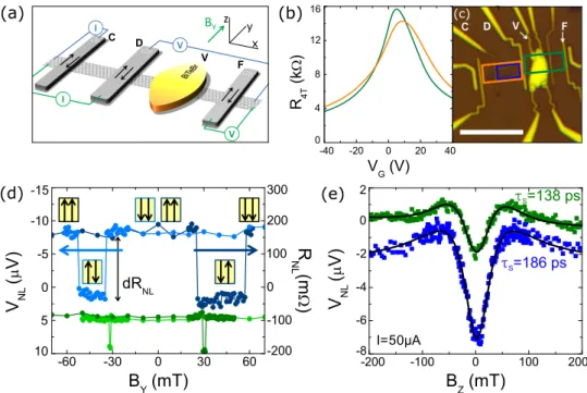
Before turning to REE in BiTeBr, we characterize spin transport behavior and polarization of FM contacts in the graphene spin valve that we use as our spin detector. Spin signal is detected by nonlocal (NL) spin injection geometry as the blue electric circuit shows inFigure 2a. Current is injected from FM contact C toward the left side of the flake, which induces spin polarization in the graphene. The spin-polarized carriers diffuse toward FM contact D which, depending on the orientation of its magnetization, is sensitive either to spin up or down chemical potential in graphene. Thus, measuring an NL voltage, VNL, between contact D and a distant reference contact, the spin polarization in graphene can be detected. Blue curves inFigure 2d show such an NL spin valve measurement as the magnetization orientation of contacts C and D is switched by an external magnetic field, BY. Because of the different coercivefields of contacts C and D, their orientation switches from↑↑via↑↓to↓↓asBYis swept down. Note that in our device with Co electrodes, the interfacial spin polarization points opposite to the FM magnetization; the black arrows show polarization rather than magnetization. The observed step in VNL has a corresponding NL resistance change, dRNL= dVNL/I≈190 mΩ(seeFigure 2d).
Applying an out-of-plane magnetic field, BZ, the spin relaxation time in the graphene channel can be determined by Hanle spin precession measurements .54 Here, diffusing spins from C to D also undergo in-plane Larmor precession along with the spin relaxation, resulting in a reduction inVNL (see blue curve inFigure 2e). In addition to the Hanle curve, a small background contribution linear inBZ, presumably caused by stray charge current, is also visible and included in thefits.
Details of the fitting process are described in theSupporting Information. Fromfitting (black solid line) the spin relaxation timeτS= 186 ps and spin relaxation lengthλS= 1.80μm were obtained, which are typical values for graphene on SiO2.50,55,56 The same NL spin valve and Hanle measurements were performed on the graphene channel with BiTeBr crystal on top, as shown by the green circuit on Figure 2a and green curves onFigure 2d,e. Very similar spin relaxation time τS= 138 ps and relaxation lengthλS= 1.64μm were determined for the BiTeBr-containing section as for the reference graphene channel. The smallerRNLamplitude for the BiTeBr-containing section is only a consequence of the longer channel length between contacts D−F than between C−D, that is, 6 μm and 4μm, respectively. Thus, we could conclude that BiTeBr does not significantly alter spin transport in graphene. This is consistent with the similarly insignificant effect of BiTeBr on the charge transport in graphene (seeFigure 2b).
With top contacts fabricated on the BiTeBr crystal (e.g., contact V onFigure 2c), vertical transport measurements were performed (seeSupporting Informationfor details), revealing a BiTeBr−graphene interface resistance RINT of 10−20 kΩ, resistance of the BiTeBr crystal of 100 Ohm with a very low bulk resistivity on the order of 10−5Ωm, and charge carrier density of approximately 1019cm−3, similar to results obtained by refs32and 33. The large interface resistance explains the BiTeBr crystal’s lack of influence on graphene spin and charge transport. It also makes an ideal configuration for spin injection into graphene due to avoiding conductance mismatch53,57,58 between graphene and the highly conductive BiTeBr.
Now we will use the graphene channel in an unconventional NL spin valve configuration, where the BiTeBr crystal serves as Figure 1. Giant Rashba SOI crystal BiTeBr. (a) Layered crystal
structure of BiTeBr, and top-down view (bottom panel). (b) Calculated Rashba-split conduction band of BiTeBr with band cut off at the Fermi energy, estimated from the high charge carrier density. Green arrows indicate subband helicity, while the color scale is they-component of the spin,SY. The inner subband (light green) has opposite helicity compared to the outer one (dark green). (c) Rashba-Edelstein effect depicted in a top-down view of the band structure at Fermi energy, not to scale. An in-plane electricfield shifts the occupied states from equilibrium (depicted as dashed circles) by kd=−eEIPτ/ℏ, whereτis the momentum scattering time. Because of the intrinsic spin splitting, more states of spin ↓ are added, corresponding to the spin orientation of the outer subband in the direction of the electricfield.
Nano Letters pubs.acs.org/NanoLett Letter
an injector electrode, using the previously characterized FM contacts as the detector. Bias current passing through the crystal can facilitate spontaneous spin polarization through REE in BiTeBr, and the current transports the polarized charge carriers into graphene where they diffuse toward the detector.
BiTeBr-injected spin polarization is observed by using two setups as depicted inFigure 3a,b, where inFigure 3a the FM detector is on the right of the BiTeBr and the current sink is on the left, and vice versa inFigure 3b. Because the electricfield orientation is different, the spins injected inFigure 3a shown in blue will have a different orientation from those inFigure 3b, shown in red. This is fundamentally different from an FM injector contact, where the spin orientation does not depend on electricfield orientation in this way.Figure 3c depicts the spin signal observed by setup (Figure 3a). In contrast to standard spin valve measurements with two FM contacts (see Figure 2d), here we only observe a single switch, instead of two, in the NL voltage as BY is swept up (orange) or down (yellow). The position of this switch (BY ≈ ±33 mT), corresponds to the switching field of the FM detector, determined in previous spin valve measurements. At negative BY, from the increase inVNLafter this switch one can conclude that the spin orientation injected from BiTeBr (blue arrows on panels a and c) becomes antiparallel with FM detector polarization.
The lack of a second switching inVNLis consistent with REE effect in bulk BiTeBr, since spin polarization injected in this way will not be affected by the applied magnetic field. At positive BY, VNL shows a lower value, where detector polarization and direction of injected spins becomes parallel
again. The same NL measurement was carried out by using an FM detector and current sink on the opposite side of BiTeBr, setup inFigure 3b. Compared to setup in Figure 3a, the NL voltage now decreases as BY is reduced (olive curve), which corresponds to reversed orientation of BiTeBr-injected spins (red arrow). This is also in agreement with REE, where a opposite spin polarization is expected if the electric field is flipped. In addition, the current direction was also reversed for both NL geometries (panels e,f), which changes the sign of the VNLjump in both cases, as is expected from REE. In terms of dRNL, the detected values are 5−10 mΩ.
To further support the origin of the signal inFigure 3being spin injection from BiTeBr, Hanle spin precession was also performed in this measurement configuration by using an out- of-planefield,BZ.Figure 4a is a schematic of the measurement, whileFigure 4b shows the Hanle curves obtained for a parallel (brown) and antiparallel (blue) configuration of the FM detector compared to the injected spin. The Hanle curves show similar spin transport characteristics as those previously measured in FM−FM spin valve configuration in graphene (Figure 2e), indicating that the detected signal is caused by polarized spins which diffuse in the graphene between the BiTeBr crystal and FM detector.
The Hanle curves inFigure 4b are slightly asymmetric. The asymmetry and offset from BZ = 0 of the maximum of the Hanle curve originates from the finite precession needed to fully align the incoming spins with the detector polarization and achieve maximum signal amplitude. This indicates an in- plane offset angle between the injected spin and FM detector.
Figure 4c shows the general effect of an injector-detector offset Figure 2.Charge and spin transport in the BiTeBr/graphene device. (a) Schematic of the device, showing the nonlocal measurement setups for spin transport in graphene. Green is used for the BiTeBr/graphene section, while blue is used as a reference graphene measurement. (b) Four terminal channel resistance as a function of gate voltage for the BiTeBr/graphene and a reference section of identical length (indicated by the same colors in panel c). Charge transport in the two sections is similar with a mobility of∼2300 and 1800 cm−2(Vs)−1, and charge neutrality pointVCNP of 6 and 12 V for the BiTeBr-containing and reference sections, respectively. (c) An optical image of the device with a 10 μm scale bar. (d) Nonlocal spin valve measurement of the sections showing typical switching with magneticfield along FM contact easy axis. Orientations of FM injector-detector pair polarization are shown in the yellow boxes. while horizontal arrows indicate the direction of sweeping magneticfield. (e) Comparison of Hanle spin precession of the BiTeBr/graphene (green) and reference (blue) sections with extracted spin relaxation times. Data corresponding to the BiTeBr/graphene sections (green) have been scaled up by a factor of 3 and manually offset by +6μV in (d) and +2μV in (e) for better visibility. Results indicate that the presence of BiTeBr has no significant influence on graphene spin transport properties.
angle on the Hanle spin precession (see Supporting Information) with the curve smoothly shifting from a symmetric (blue) to an antisymmetric (green) one in increments of 10°. Byfitting, a small angle of 6°is obtained for the data in Figure 4b. We also present a measurement in another device (Device 2) in Figure 4d, where a more noticeable offset of approximately 37°is obtained. The device is shown in the inset, where the BiTeBr crystal features Au top contacts. Dotted lines represent the extent of graphene in the device. On the data set, the red curve is the asymmetric fit, while a reference curve of 0°offset is shown as a dashed black line to visually emphasize the difference.
In the case of an FM contact, the orientation of injected or detected spin depends on the magnetization, typically along the easy axis along the length of the FM contact. On the other hand, when injecting using the BiTeBr crystal due to REE, polarization will be perpendicular to the electric field driving charge transport. The BiTeBr crystals have relatively small thickness (100 nm) compared to lateral size (fewμm), as well
as a low resistance compared to the graphene and interface resistance. This suggests that the electricfield within them will be predominantly in-plane. This assumption is also supported byfinite element simulation on a simplified geometric model of our devices (see Supporting Information). However, the orientation of the electricfield within thexy-plane will depend on the geometry of the irregularly shaped crystal, the position of the metallic top contact, and that of the BiTeBr−graphene interface. For Device 2, in the inset in Figure 4d the green curved arrow depicts the expected current flow and electric field lines in BiTeBr, determining the angle of injected spins (shown in red).
To further characterize the spin signal injected from BiTeBr, Figure 5a shows nonlocal spin valve switching of the signal, measured at different values of the backgate voltage, ranging from −40 to 40 V, where the curves are offset in y-axis for clarity. Since the charge neutrality point of the graphene section is at approximately 6 V, this demonstrates that the observed transition does not change sign while transport Figure 3.Spin injection from BiTeBr to graphene and its dependence on electricfield orientation. (a,b) Measurement schematics of spin injection from BiTeBr crystal and nonlocal detection using FM contact on opposite sides of the device to demonstrate bias orientation dependence. (c,d) Spin-polarized signal detected nonlocally using the setup in (a,b), respectively, using positive bias current. Horizontal arrows indicate the direction of magneticfield sweep. The injected spin polarization is opposite on (c) compared to (d). (e,f) The same measurement using negative bias current. The observed spin polarization injected into graphene is the same as in (c,d). The parallel and antiparallel spin configurations are indicated in the yellow boxes.
Nano Letters pubs.acs.org/NanoLett Letter
changes from electron-like carriers to hole-like ones and cannot be attributed to local Hall effect in FM detector contact. The signal amplitude is seen to change very little with backgate voltage with values from additional measurements represented in panel b. This is not surprising, considering the BiTeBr has relatively high charge carrier density, preventing significant gate dependence of resistance, and the resistance of the BiTeBr−graphene interface is also observed to change by no more than a factor of 2 over this gate voltage range.Figure 5c depicts a bias current dependence of the amplitude of signals observed on both contacts D (blue) and F (red). Signal amplitude is extracted from both NL spin valve measurements (rectangles) as well as out-of-plane Hanle spin precession measurements (triangles). For the latter, values equal to double the Hanle peak amplitudes were plotted to correspond with the NL spin valve amplitudes. Note the sign change in the signal with change of bias direction, as also seen inFigure 3.
This can be explained by REE-induced nonequilibrium between spin-dependent chemical potentials in BiTeBr.
Further discussion can be found in the Supporting Information.
The lack of SOI enhancement in graphene under the BiTeBr crystal, the single switching observed in NL measurements while injecting from BiTeBr, the observation of Hanle spin precession, and the gate dependence of the NL signal all support the notion that the spin polarization detected in graphene originates from the bulk of BiTeBr. We have also attempted to detect a NL signal in graphene while passing bias current through the BiTeBr crystal only (using two metallic
top contacts) but we could not detect a similar switching signal in this case. This is also consistent with the large BiTeBr/
graphene interface preventing diffusion of spins from one material to the other.
We can treat the BiTeBr−interface−graphene structure similarly to a FM-tunnel barrier−graphene structure and calculate an interfacial spin polarization .59Using bias currents of between 40−60 μA, the experimentally observed polar- ization in Device 1 is 0.09% and 0.07% when detecting on contact D and F, respectively, and 0.08% in Device 2 while using a bias current of 80μA. We have constructed a tunneling model (detailed in Supporting Information) to calculate the expected current polarization of electrons, having net spin polarization due to REE, tunneling from BiTeBr into graphene.
The model takes into account the 3D band structure of BiTeBr, the position of the Fermi level, μBiTeBr ≈ 50 meV, estimated from transport data, and the shift in occupation of electron states in BiTeBr due to the internal electricfield,EIP. For the Rashba parameter, αR ≈ 2 eVÅ was used.30 The momentum relaxation time τ can be approximated from the Drude model to be 5.3 × 10⁻¹⁴ s, reasonably close to that obtained in ref33.EIPcan be estimated from BiTeBr resistivity and shape and the bias current. For Device 1, EIP fields of approximately 3500 and 3000 V/m are obtained when detecting on contact D and F respectively. Using these values, the tunneling model predicts a spin polarization of the injected current ofP= 0.095% and 0.083% for detecting on contact D and F, respectively, which is in good agreement with the Figure 4.Hanle spin precession of injected spin polarization from BiTeBr. (a) Schematic of device with spin injection from BiTeBr in out-of-plane magneticfieldBZresulting in Hanle spin precession in the graphene. (b) Hanle spin precession curves as measured using the setup in (a) with a 60 μA bias current showing both parallel (brown) and antiparallel (blue) configurations of the FM contact and injected spin. There is a slight asymmetry in the signal, indicating an approximately 6°injector-detector in-plane offset angle. (c) Theoretical Hanle curves for different injector- detector offset angles. The symmetric curve (blue) corresponds to the fully parallel configuration, while the antisymmetric curve (green) corresponds to the perpendicular configuration with intermediary curves in increments of 10°. (d) Hanle measurement on a second device, shown in the inset image. Fitting indicates a greater offset angle of approximately 37°. For comparison, the expected curve for a 0°offset is shown as a dashed black line.
experimentally observed values. We see the same agreement for the results obtained in Device 2 as well.
Aside from REE, a competing phenomenon that could result in spin injection into graphene is the Spin Hall Effect (SHE)15,60 also taking place in bulk BiTeBr, caused by the strong intrinsic SOI. The SHE has been studied extensively in TMD/graphene heterostructures.16,17,61,62,64
In the case of SHE, the same electric field EIP is expected to create spin currents along thez-direction, resulting in spin accumulation at the top and bottom of the BiTeBr crystal. The orientation of spins would also be perpendicular toEIP, as is the case with REE. We estimate the expected SHE polarization following ref 63 (detailed in Supporting Information). Using the exper- imentally observed polarization values of ∼0.1% and taking into consideration the measurement uncertainties, we obtain an estimated range for the BiTeBr spin Hall angle,αSHE, to be within 1.11−5.71. However, because SHE describes a conversion from charge current to spin current,αSHE should be limited to|αSHE| ≤ 1. Since even the lower bound of our estimate range is over unity, we consider that REE is a more likely explanation for our experimental results.
The REE and its inverse have been experimentally explored in interfaces between thin films where z-symmetry is broken18,65−68 and also more recently in graphene hetero- structures. In these cases, the REE mechanism originates from proximity-induced SOI in graphene at the interface with another material, such as WS2,22WSe2,69MoS2,17MoTe2,70,71 TaS2,72or topological insulators.21,73In contrast, in our work, due to a large interface resistance, there is no proximity SOI enhancement in the graphene, and the observed spin polarization originates from REE within the BiTeBr bulk.
The lack of a sign change in the gate dependence of the signal
further supports this, as proximity-induced REE in graphene is expected to give rise to a sign change as the carrier density is tuned from the electron to the hole region.70,73,74,75
In addition, we did not observe any sign of weak antilocalization in our devices at temperatures down to 50 mK.
In our tunneling model, the REE-induced current polar- ization is inversely proportional to the Fermi level in the BiTeBr band, which is in agreement with REE theory .44Thus, the polarization should strongly depend on the 3D electron density in BiTeBr, that is,P∼n−2/3. The used BiTeBr crystals feature a very high charge carrier density with a Fermi energy of around 50 meV. Further development of bulk crystal growth techniques could result in lower carrier densities, which leads to an increase in polarization magnitude. Existing works already show a variation of approximately 1 order of magnitude in the carrier density of bulk crystals .33,76An improvement of 1 order of magnitude would already produce polarizations comparable to our FM contacts, thus allowing FM injectors to be replaced by BiTeBr. Another promising alternative could be provided by few-layer BiTeBr, allowing for effective gating.
Recently a method for exfoliating single-layer BiTeIflakes has been reported .77
■
CONCLUSIONWe have demonstrated the electrical creation and control of spin polarization in the giant Rashba spin−orbit crystal BiTeBr at room temperature. Application of an electric bias generates spin polarization in the bulk bands of BiTeBr due to the Rashba-Edelstein effect where the magnitude and direction are determined by the electric current strength and direction. This spin polarization in BiTeBr is demonstrated by injecting into the graphene channel and detecting in a spin valve device Figure 5.Gate and bias dependence of injected spin signal from BiTeBr. (a) Nonlocal spin signal switching using an in-planefieldBYat various backgate voltages showing modest change in signal amplitude dRNL. The data traces are manually stacked using 30 mΩoffsets for better visibility.
(b) The dRNLvalues plotted as a function of backgate voltage. The signal has the same orientation under both electron and hole dominated transport in graphene. (c) DC bias current dependence of the spin injection signal amplitude using FM detector contacts D (blue) and F (red) of Device 1. Triangles represent information extracted from Hanle spin precession, and rectangles represent nonlocal spin signal data for the same respective sections.
Nano Letters pubs.acs.org/NanoLett Letter
utilizing reliable nonlocal spin transport and Hanle spin precession measurements. The detailed measurement of the spin signal with different bias current directions and gate voltages proves the robustness of the spin polarization, which is in agreement with current-induced spin polarization from the bulk Rashba spin-split bands of BiTeBr crystal. Thesefindings prove that Rashba spin−orbit crystals are an attractive novel building block for various spintronic applications since they can serve as an all-electrically controlled spin polarization source. Further enhancement and tuning of the current- induced spin polarization is within reach by controlling the Fermi-level position with doping. These advances in electrical control and tunability of spin sources will open new avenues to replace ferromagnetic components in integrated spintronic memory and logic technologies.
■
ASSOCIATED CONTENT*sı Supporting Information
The Supporting Information is available free of charge at https://pubs.acs.org/doi/10.1021/acs.nanolett.0c00458.
Device fabrication and experimental methods, detailed charge and spin transport characterization, extraction of spin transport characteristics, determination of spin polarization, method for extracting angle offset of polarization from Hanle spin precession data, finite element simulation of electricfield inside BiTeBr, tunnel junction modeling of the BiTeBr/graphene interface, and estimation of expected REE and SHE polarization and comparison with experimental results (PDF)
■
AUTHOR INFORMATION Corresponding AuthorsPeter Makḱ −Department of Physics, Budapest University of Technology and Economics and Nanoelectronics‘Momentum’ Research Group of the Hungarian Academy of Sciences, 1111 Budapest, Hungary; orcid.org/0000-0001-7637-4672;
Email:peter.makk@mail.bme.hu
Saroj Prasad Dash−Department of Microtechnology and Nanoscience, Chalmers University of Technology, SE-41296 Göteborg, Sweden; orcid.org/0000-0001-7931-4843;
Email:saroj.dash@chalmers.se Authors
Zoltán Kovács-Krausz −Department of Physics, Budapest University of Technology and Economics and Nanoelectronics
‘Momentum’Research Group of the Hungarian Academy of Sciences, 1111 Budapest, Hungary; orcid.org/0000-0001- 5821-6195
Anamul Md Hoque−Department of Microtechnology and Nanoscience, Chalmers University of Technology, SE-41296 Göteborg, Sweden
Bálint Szentpéteri− Department of Physics, Budapest University of Technology and Economics and Nanoelectronics
‘Momentum’Research Group of the Hungarian Academy of Sciences, 1111 Budapest, Hungary
Mátyás Kocsis−Department of Physics, Budapest University of Technology and Economics and Nanoelectronics‘Momentum’ Research Group of the Hungarian Academy of Sciences, 1111 Budapest, Hungary
Bálint Fülöp− Department of Physics, Budapest University of Technology and Economics and Nanoelectronics‘Momentum’
Research Group of the Hungarian Academy of Sciences, 1111 Budapest, Hungary
Michael Vasilievich Yakushev−M.N. Miheev Institute of Metal Physics and Institute of Solid State Chemistry, Ural Branch of the Russian Academy of Science, 620108 Ekaterinburg, Russia; Ural Federal University, Ekaterinburg 620002, Russia
Tatyana Vladimirovna Kuznetsova−M.N. Miheev Institute of Metal Physics, Ural Branch of the Russian Academy of Science, 620108 Ekaterinburg, Russia; Ural Federal University, Ekaterinburg 620002, Russia
Oleg Evgenevich Tereshchenko− St. Petersburg State University, 198504 St. Petersburg, Russia; A. V. Rzhanov Institute of Semiconductor Physics, 630090 Novosibirsk, Russia;
Novosibirsk State University, 630090 Novosibirsk, Russia Konstantin Aleksandrovich Kokh−St. Petersburg State
University, 198504 St. Petersburg, Russia; Novosibirsk State University, 630090 Novosibirsk, Russia; V. S. Sobolev Institute of Geology and Mineralogy, 630090 Novosibirsk, Russia István Endre Lukács−Center for Energy Research, Institute of
Technical Physics and Material Science, H-1121 Budapest, Hungary
Takashi Taniguchi−National Institute for Material Science, Tsukuba 305-0044, Japan; orcid.org/0000-0002-1467- 3105
Kenji Watanabe− National Institute for Material Science, Tsukuba 305-0044, Japan; orcid.org/0000-0003-3701- 8119
Szabolcs Csonka−Department of Physics, Budapest University of Technology and Economics and Nanoelectronics‘Momentum’ Research Group of the Hungarian Academy of Sciences, 1111 Budapest, Hungary
Complete contact information is available at:
https://pubs.acs.org/10.1021/acs.nanolett.0c00458
Author Contributions
Z.K.K. and B.S. fabricated the devices with help from A.M.H., B.F., and M.K. The growth and primary characterization of the BiTeBr single crystals was carried out by K.A.K., O.E.T., T.V.K., and M.V.Y. The hBN crystals were provided by T.T.
and K.W. Z.K.K., B.S., and A.M.H. performed the measure- ments. Data analysis was performed by Z.K.K., B.S., A.M.H., P.M., and S.C. Tunneling model was created by B.S. with help from P.M., S.C., and M.K. All authors contributed to the manuscript and discussions. S.C., S.P.D., and P.M. planned and guided the project.
Notes
The authors declare no competingfinancial interest.
■
ACKNOWLEDGMENTSThe authors thank D. Khokhiriakov and B. Karpiak for their help in device fabrication and measurements, M. G. Beckerné, F. Fülöp, M. Hajdu for their technical support, and T. Fehér, L.
Oroszlány, C. Schönenberger, S. O. Valenzuela, A. Virosztek, and I. Zutic for useful discussions. This work has received funding and support from Topograph, CA16218 by COST, the Flag-ERA iSpinText project, the ÚNKP-19-3-II-BME-303 New National Excellence Program of the Ministry of Human Capacities, from the OTKA FK-123894 and OTKA NN- 127900 grants, and RFBR project number 19-29-12061. P.M.
acknowledges support from the Bolyai Fellowship, the Marie Curie grant, and the National Research, Development, and
Innovation Fund of Hungary within the Quantum Technology National Excellence Program (Project Nr. 2017-1.2.1-NKP- 2017-00001). S.P.D. acknowledges funding from Swedish Research Council VR No. 2015-06813 and 2016-03658.
M.V.Y. and T.V.K. were supported by the Ministry of Science and Higher Education of the Russian Federation (“Spin” No AAAA-A18-118020290104-2) whereas O.E.T. and K.A.K. were supported by the Russian Science Foundation (No 17-12- 01047) and Saint Petersburg State University (Project ID 51126254). K.W. and T.T. acknowledge support from the Elemental Strategy Initiative conducted by the MEXT, Japan and the CREST (JPMJCR15F3), JST.
■
(1) Manchon, A.; Koo, H. C.; Nitta, J.; Frolov, S. M.; Duine, R. A.REFERENCES New perspectives for Rashba spin−orbit coupling.Nat. Mater.2015, 14, 871−882.(2) Kane, C. L.; Mele, E. J. Quantum Spin Hall Effect in Graphene.
Phys. Rev. Lett.2005,95, 226801.
(3) Bernevig, B. A.; Zhang, S.-C. Quantum Spin Hall Effect.Phys.
Rev. Lett.2006,96, 106802.
(4) Konig, M.; Buhmann, H.; Molenkamp, L. W.; Hughes, T.; Liu, C.-X.; Qi, X.-L.; Zhang, S.-C. The Quantum Spin Hall Effect: Theory and Experiment.J. Phys. Soc. Jpn.2008,77, 031007.
(5) Fu, L.; Kane, C. L. Superconducting Proximity Effect and Majorana Fermions at the Surface of a Topological Insulator.Phys.
Rev. Lett.2008,100, 096407.
(6) Sau, J. D.; Lutchyn, R. M.; Tewari, S.; Das Sarma, S. Generic New Platform for Topological Quantum Computation Using Semiconductor Heterostructures.Phys. Rev. Lett.2010,104, 040502.
(7) Mourik, V.; Zuo, K.; Frolov, S. M.; Plissard, S. R.; Bakkers, E. P.
A. M.; Kouwenhoven, L. P. Signatures of Majorana Fermions in Hybrid Superconductor-Semiconductor Nanowire Devices. Science 2012,336, 1003−1007.
(8) Lutchyn, R. M.; Bakkers, E. P. A. M.; Kouwenhoven, L. P.;
Krogstrup, P.; Marcus, C. M.; Oreg, Y. Majorana zero modes in superconductor−semiconductor heterostructures. Nature Reviews Materials2018,3, 52−68.
(9) Soumyanarayanan, A.; Reyren, N.; Fert, A.; Panagopoulos, C.
Emergent phenomena induced by spin−orbit coupling at surfaces and interfaces.Nature2016,539, 509−517.
(10) Schaibley, J.; Yu, H.; Clark, G.; Rivera, P.; Ross, J.; Seyler, K.;
Yao, W.; Xu, X. Valleytronics in 2D materials. Nature Reviews Materials2016,1, 16055.
(11) van der Wiel, W. G.; De Franceschi, S.; Elzerman, J. M.;
Fujisawa, T.; Tarucha, S.; Kouwenhoven, L. P. quantum dots.Rev.
Mod. Phys.2002,75, 1−22.
(12) Kloeffel, C.; Loss, D. Prospects for Spin-Based Quantum Computing in Quantum Dots.Annu. Rev. Condens. Matter Phys.2013, 4, 51−81.
(13) Chernyshov, A.; Overby, M.; Liu, X.; Furdyna, J. K.; Lyanda- Geller, Y.; Rokhinson, L. P. Evidence for reversible control of magnetization in a ferromagnetic material by means of spin−orbit magnetic field.Nat. Phys.2009,5, 656−659.
(14) Manchon, A.; Železný, J.; Miron, I. M.; Jungwirth, T.; Sinova, J.; Thiaville, A.; Garello, K.; Gambardella, P. Current-induced spin- orbit torques in ferromagnetic and antiferromagnetic systems. Rev.
Mod. Phys.2019,91, 035004.
(15) Sinova, J.; Valenzuela, S. O.; Wunderlich, J.; Back, C. H.;
Jungwirth, T. Spin Hall effects.Rev. Mod. Phys.2015,87, 1213−1260.
(16) Zhao, B.; Khokhriakov, D.; Zhang, Y.; Fu, H.; Karpiak, B.;
Hoque, A. M.; Xu, X.; Jiang, Y.; Yan, B.; Dash, S. P. Observation of charge to spin conversion in Weyl semimetal WTe2 at room tepmerature.Phys. Rev. Research2020,2, 013286.
(17) Safeer, C. K.; Ingla-Aynés, J.; Herling, F.; Garcia, J. H.; Vila, M.;
Ontoso, N.; Calvo, M. R.; Roche, S.; Hueso, L. E.; Casanova, F. Room temperature spin Hall effect in graphene/MoS2 van der Waals heterostructures.Nano Lett.2019,19, 1074−1082.
(18) Nakayama, H.; Kanno, Y.; An, H.; Tashiro, T.; Haku, S.;
Nomura, A.; Ando, K. Rashba-Edelstein Magnetoresistance in Metallic Heterostructures.Phys. Rev. Lett.2016,117, 1−15.
(19) Rojas-Sánchez, J.-C.; Oyarzún, S.; Fu, Y.; Marty, A.; Vergnaud, C.; Gambarelli, S.; Vila, L.; Jamet, M.; Ohtsubo, Y.; Taleb-Ibrahimi, A.; Le Fèvre, P.; Bertran, F.; Reyren, N.; George, J.-M.; Fert, A. Spin to Charge Conversion at Room Temperature by Spin Pumping into a New Type of Topological Insulator:α-Sn Films.Phys. Rev. Lett.2016, 116, 096602.
(20) Lesne, E.; et al. Highly efficient and tunable spin-to-charge conversion through Rashba coupling at oxide interfaces.Nat. Mater.
2016,15, 1261−1266.
(21) Rodriguez-Vega, M.; Schwiete, G.; Sinova, J.; Rossi, E. Giant Edelstein effect in topological-insulator−graphene heterostructures.
Phys. Rev. B: Condens. Matter Mater. Phys.2017,96, 235419.
(22) Ghiasi, T. S.; Kaverzin, A. A.; Blah, P. J.; van Wees, B. J.
Charge-to-Spin Conversion by the Rashba−Edelstein Effect in Two- Dimensional van der Waals Heterostructures up to Room Temper- ature.Nano Lett.2019,19, 5959−5966.
(23) Benítez, L. A.; Torres, W. S.; Sierra, J. F.; Timmermans, M.;
Garcia, J. H.; Roche, S.; Costache, M. V.; Valenzuela, S. O. Tunable room-temperature spin galvanic and spin Hall effects in van der Waals heterostructures.Nat. Mater.2020,19, 170−175.
(24) Vaklinova, K.; Hoyer, A.; Burghard, M.; Kern, K. Current- Induced Spin Polarization in Topological Insulator−Graphene Heterostructures.Nano Lett.2016,16, 2595−2602.
(25) Ishizaka, K.; et al. Giant Rashba-type spin splitting in bulk BiTeI.Nat. Mater.2011,10, 521−6.
(26) Bahramy, M. S.; Arita, R.; Nagaosa, N. Origin of giant bulk Rashba splitting: Application to BiTeI.Phys. Rev. B: Condens. Matter Mater. Phys.2011,84, 041202.
(27) Eremeev, S. V.; Rusinov, I. P.; Nechaev, I. A.; Chulkov, E. V.
Rashba split surface states in BiTeBr.New J. Phys.2013,15, 075015.
(28) Maaß, H.; Bentmann, H.; Seibel, C.; Tusche, C.; Eremeev, S.
V.; Peixoto, T. R. F.; Tereshchenko, O. E.; Kokh, K. A.; Chulkov, E.
V.; Kirschner, J.; Reinert, F. Spin-texture inversion in the giant Rashba semiconductor BiTeI.Nat. Commun.2016,7, 11621.
(29) Xin, J.; Fu, C.-G.; Shi, W.-J.; Li, G.-W.; Auffermann, G.; Qi, Y.- P.; Zhu, T.-J.; Zhao, X.-B.; Felser, C. Synthesis and thermoelectric properties of Rashba semiconductor BiTeBr with intensive texture.
Rare Met.2018,37, 274.
(30) Sakano, M.; Bahramy, M. S.; Katayama, A.; Shimojima, T.;
Murakawa, H.; Kaneko, Y.; Malaeb, W.; Shin, S.; Ono, K.;
Kumigashira, H.; Arita, R.; Nagaosa, N.; Hwang, H. Y.; Tokura, Y.;
Ishizaka, K. Strongly Spin-Orbit Coupled Two-Dimensional Electron Gas Emerging near the Surface of Polar Semiconductors.Phys. Rev.
Lett.2013,110, 107204.
(31) Akrap, A.; Teyssier, J.; Magrez, A.; Bugnon, P.; Berger, H.;
Kuzmenko, A. B.; van der Marel, D. Optical properties of BiTeBr and BiTeCl.Phys. Rev. B: Condens. Matter Mater. Phys.2014,90, 035201.
(32) Martin, C.; Suslov, A. V.; Buvaev, S.; Hebard, A. F.; Bugnon, P.;
Berger, H.; Magrez, A.; Tanner, D. B. Experimental determination of the bulk Rashba parameters in BiTeBr. Europhys. Lett. 2016, 116, 57003.
(33) Ideue, T.; Hamamoto, K.; Koshikawa, S.; Ezawa, M.; Shimizu, S.; Kaneko, Y.; Tokura, Y.; Nagaosa, N.; Iwasa, Y. Bulk rectification effect in a polar semiconductor.Nat. Phys.2017,13, 578−583.
(34) Bahramy, M.; Yang, B.-J.; Arita, R.; Nagaosa, N. Emergence of non-centrosymmetric topological insulating phase in BiTeI under pressure.Nat. Commun.2012,3, 679.
(35) Chen, Y.; Xi, X.; Yim, W.-L.; Peng, F.; Wang, Y.; Wang, H.; ma, Y.; Liu, G.; Sun, C.; Ma, C.; Chen, Z.; Berger, H. High-Pressure Phase Transitions and Structures of Topological Insulator BiTeI. J. Phys.
Chem. C2013,117, 25677−25683.
(36) Crassee, I.; Borondics, F.; Tran, M. K.; Autès, G.; Magrez, A.;
Bugnon, P.; Berger, H.; Teyssier, J.; Yazyev, O. V.; Orlita, M.; et al.
BiTeCl and BiTeBr: A comparative high-pressure optical study.Phys.
Rev. B: Condens. Matter Mater. Phys.2017,95, 045201.
Nano Letters pubs.acs.org/NanoLett Letter
(37) Rusinov, I.; Menshchikova, T.; Sklyadneva, I.; Heid, R.;
Bohnen, K.; Chulkov, E. Pressure effects on crystal and electronic structure of bismuth tellurohalides.New J. Phys.2016,18, 113003.
(38) Ohmura, A.; Higuchi, Y.; Ochiai, T.; Kanou, M.; Nakano, S.;
Ishikawa, F.; Nakayama, A.; Yamada, Y.; Sasagawa, T. Investigation of topological phase transition in BiTeBr under high pressure.J. Phys.:
Conf. Ser.2017,950, 042036.
(39) Jin, M. L.; Sun, F.; Xing, L. Y.; Zhang, S. J.; Feng, S. M.; Kong, P. P.; Li, W. M.; Wang, X. C.; Zhu, J. L.; Long, Y. W.; Bai, H. Y.; Gu, C. Z.; Yu, R. C.; Yang, W. G.; Shen, G. Y.; Zhao, Y. S.; Mao, H. K.;
Jin, C. Q. Superconductivity Bordering Rashba Type Topological Transition.Sci. Rep.2017,7, 39699.
(40) Jin, M.; Zhang, S.; Xing, L.; Li, W.; Zhao, G.; Wang, X.; Long, Y.; Li, X.; Bai, H.; Gu, C.; Jin, C. Pressure-induced superconductivity and quantum phase transitions in the Rashba material BiTeCl.J. Phys.
Chem. Solids2019,128, 211−217.
(41) Bawden, L.; Riley, J. M.; Kim, C. H.; Sankar, R.; Monkman, E.
J.; Shai, D. E.; Wei, H. I.; Lochocki, E. B.; Wells, J. W.; Meevasana, W.; et al. Hierarchical spin-orbital polarization of a giant Rashba system.Science Advances2015,1, No. e1500495.
(42) Shevelkov, A.; Dikarev, E.; Shpanchenko, R.; Popovkin, B.
Crystal Structures of Bismuth Tellurohalides BiTeX (X = Cl, Br, I) from X-Ray Powder Diffraction Data.J. Solid State Chem.1995,114, 379−384.
(43) Aronov, A.; Lyanda-Geller, Y.; Pikus, G. Spin polarization of electrons by an electric current.Sov. Phys. JETP1991,73, 537−541.
(44) Edelstein, V. M. Spin polarization of conduction electrons induced by electric current in two-dimensional asymmetric electron systems.Solid State Commun.1990,73, 233−235.
(45) Han, W.; Kawakami, R. K.; Gmitra, M.; Fabian, J. Graphene spintronics.Nat. Nanotechnol.2014,9, 794−807.
(46) Tombros, N.; Jozsa, C.; Popinciuc, M.; Jonkman, H. T.; van Wees, B. J. Electronic spin transport and spin precession in single graphene layers at room temperature.Nature2007,448, 571−574.
(47) Dery, H.; Wu, H.; Ciftcioglu, B.; Huang, M.; Song, Y.;
Kawakami, R.; Shi, J.; Krivorotov, I.; Zutic, I.; Sham, L. J.
Nanospintronics Based on Magnetologic Gates.IEEE Trans. Electron Devices2012,59, 259−262.
(48) Popinciuc, M.; Józsa, C.; Zomer, P. J.; Tombros, N.; Veligura, A.; Jonkman, H. T.; van Wees, B. J. Electronic spin transport in graphene field-effect transistors.Phys. Rev. B: Condens. Matter Mater.
Phys.2009,80, 214427.
(49) Han, W.; Pi, K.; McCreary, K. M.; Li, Y.; Wong, J. J. I.; Swartz, A. G.; Kawakami, R. K. Tunneling Spin Injection into Single Layer Graphene.Phys. Rev. Lett.2010,105, 167202.
(50) Han, W.; McCreary, K.; Pi, K.; Wang, W.; Li, Y.; Wen, H.;
Chen, J.; Kawakami, R. Spin transport and relaxation in graphene.J.
Magn. Magn. Mater.2012,324, 369−381.
(51) Roche, S.; Valenzuela, S. O. Graphene spintronics: puzzling controversies and challenges for spin manipulation.J. Phys. D: Appl.
Phys.2014,47, 094011.
(52) Drögeler, M.; Volmer, F.; Wolter, M.; Terrés, B.; Watanabe, K.;
Taniguchi, T.; Güntherodt, G.; Stampfer, C.; Beschoten, B.
Nanosecond Spin Lifetimes in Single- and Few-Layer Graphene−
hBN Heterostructures at Room Temperature.Nano Lett.2014,14, 6050−6055.
(53) Tombros, N.; Jozsa, C.; Popinciuc, M.; Jonkman, H. T.; van Wees, B. J. Electronic spin transport and spin precession in single graphene layers at room temperature.Nature2007,448, 571−574.
(54) Jedema, F. J.; Costache, M. V.; Heersche, H. B.; Baselmans, J. J.
A.; van Wees, B. J. Electrical detection of spin accumulation and spin precession at room temperature in metallic spin valves. Appl. Phys.
Lett.2002,81, 5162−5164.
(55) Sosenko, E.; Wei, H.; Aji, V. Effect of contacts on spin lifetime measurements in graphene.Phys. Rev. B: Condens. Matter Mater. Phys.
2014,89, 245436.
(56) Han, W.; Pi, K.; Bao, W.; McCreary, K. M.; Li, Y.; Wang, W.
H.; Lau, C. N.; Kawakami, R. K. Electrical detection of spin
precession in single layer graphene spin valves with transparent contacts.Appl. Phys. Lett.2009,94, 222109.
(57) Schmidt, G.; Ferrand, D.; Molenkamp, L. W.; Filip, A. T.; van Wees, B. J. Fundamental obstacle for electrical spin injection from a ferromagnetic metal into a diffusive semiconductor. Phys. Rev. B:
Condens. Matter Mater. Phys.2000,62, R4790−R4793.
(58) Fert, A.; Jaffres, H. Conditions for efficient spin injection from a ferromagnetic metal into a semiconductor. Phys. Rev. B: Condens.
Matter Mater. Phys.2001,64, 184420.
(59) Valet, T.; Fert, A. Theory of the perpendicular magneto- resistance in magnetic multilayers. Phys. Rev. B: Condens. Matter Mater. Phys.1993,48, 7099−7113.
(60) Vignale, G. Ten Years of Spin Hall Effect.J. Supercond. Novel Magn.2010,23, 3.
(61) Avsar, A.; Tan, J. Y.; Taychatanapat, T.; Balakrishnan, J.; Koon, G.; Yeo, Y.; Lahiri, J.; Carvalho, A.; Rodin, A. S.; O’Farrell, E.; et al.
Spin−orbit proximity effect in graphene.Nat. Commun.2014,5, 4875.
(62) Garcia, J. H.; Cummings, A. W.; Roche, S. Spin Hall Effect and Weak Antilocalization in Graphene/Transition Metal Dichalcogenide Heterostructures.Nano Lett.2017,17, 5078−5083.
(63) Dyakonov, M. I. Spin Hall Effect. Future Trends in Microelectronics2010, 251−263.
(64) Milletarı, M.; Offidani, M.; Ferreira, A.; Raimondi, R. Covariant̀ Conservation Laws and the Spin Hall Effect in Dirac-Rashba Systems.
Phys. Rev. Lett.2017,119, 246801.
(65) Sanchez, J. C. R.; Vila, L.; Desfonds, G.; Gambarelli, S.; Attane, J. P.; De Teresa, J. M.; Magen, C.; Fert, A. Spin-to-charge conversion using Rashba coupling at the interface between non-magnetic materials.Nat. Commun.2013,4, 2944.
(66) Isasa, M.; Martínez-Velarte, M. C.; Villamor, E.; Magén, C.;
Morellón, L.; De Teresa, J. M.; Ibarra, M. R.; Vignale, G.; Chulkov, E.
V.; Krasovskii, E. E.; et al. Origin of inverse Rashba-Edelstein effect detected at the Cu/Bi interface using lateral spin valves.Phys. Rev. B:
Condens. Matter Mater. Phys.2016,93, 014420.
(67) Auvray, F.; Puebla, J.; Xu, M.; Rana, B.; Hashizume, D.; Otani, Y. Spin accumulation at nonmagnetic interface induced by direct Rashba−Edelstein effect. J. Mater. Sci.: Mater. Electron. 2018, 29, 15664−15670.
(68) Du, Y.; Karube, S.; Gamou, H.; Ryu, J.; Takahashi, S.; Kohda, M.; Nitta, J.Anomalous spin orbit torques with large Rashba spin orbit coupling in epitaxial Pt/Co bilayers. 2018, arXiv:1807.10867. arXiv.org e-Print archive.https://arxiv.org/abs/1807.10867 (accessed Jun 03, 2020).
(69) Avsar, A.; Unuchek, D.; Liu, J.; Sanchez, O. L.; Watanabe, K.;
Taniguchi, T.; Özyilmaz, B.; Kis, A. Optospintronics in Graphene via Proximity Coupling.ACS Nano2017,11, 11678−11686.
(70) Hoque, A.; Khokhriakov, D.; Karpiak, B.; Dash, S.All-electrical creation and control of giant spin-galvanic effect in 1T-MoTe2/graphene heterostructures at room temperature. 2019, arXiv:1908.09367.
arXiv.org e-Print archive.https://arxiv.org/abs/1908.09367(accessed Jun 03, 2020).
(71) Safeer, C. K.; Ontoso, N.; Ingla-Aynés, J.; Herling, F.; Pham, V.
T.; Kurzmann, A.; Ensslin, K.; Chuvilin, A.; Robredo, I.; Vergniory, M. G.; de Juan, F.; Hueso, L. E.; Calvo, M. R.; Casanova, F. Large multi-directional spin-to-charge conversion in low symmetry semi- metal MoTe2at room temperature.Nano Lett.2019,19, 8758−8766.
(72) Li, L.; Zhang, J.; Myeong, G.; Shin, W.; Lim, H.; Kim, B.; Kim, S.; Jin, T.; Cavill, S.; Kim, B. S.; Kim, C.; Lischner, J.; Ferreira, A.;
Cho, S. Gate-Tunable Reversible Rashba−Edelstein Effect in a Few- Layer Graphene/2H-TaS2 Heterostructure at Room Temperature.
ACS Nano2020,14, 5251−5259.
(73) Khokhriakov, D.; Hoque, A. M.; Karpiak, B.; Dash, S. P.Giant and Gate-tunable Spin-Galvanic Effect in Graphene Topological insulator van der Waals Heterostructures at Room Temperature. 2019, arXiv:1910.06760. arXiv.org e-Print archive. https://arxiv.org/abs/
1910.06760(accessed Jun 03, 2020).
(74) Dyrdał, A.; Barnaś, J.; Dugaev, V. K. Current-induced spin polarization in graphene due to Rashba spin-orbit interaction.Phys.
Rev. B: Condens. Matter Mater. Phys.2014,89, 075422.
(75) Offidani, M.; Milletarı̀, M.; Raimondi, R.; Ferreira, A. Optimal Charge-to-Spin Conversion in Graphene on Transition-Metal Dichalcogenides.Phys. Rev. Lett.2017,119, 196801.
(76) Kanou, M.; Sasagawa, T. Crystal growth and electronic properties of a 3D Rashba material, BiTeI, with adjusted carrier concentrations.J. Phys.: Condens. Matter2013,25, 135801.
(77) Fülöp, B.; Tajkov, Z.; Pető, J.; Kun, P.; Koltai, J.; Oroszlány, L.;
Tóvári, E.; Murakawa, H.; Tokura, Y.; Bordács, S.; Tapasztó, L.;
Csonka, S. Exfoliation of single layer BiTeI flakes.2D Mater.2018,5, 031013.
Nano Letters pubs.acs.org/NanoLett Letter