Editors’ Suggestion
Large spin relaxation anisotropy and valley-Zeeman spin-orbit coupling in WSe
2/graphene/h-BN heterostructures
Simon Zihlmann,1,*Aron W. Cummings,2Jose H. Garcia,2Máté Kedves,3Kenji Watanabe,4Takashi Taniguchi,4 Christian Schönenberger,1and Péter Makk1,3,†
1Department of Physics, University of Basel, Klingelbergstrasse 82, CH-4056 Basel, Switzerland
2Catalan Institute of Nanoscience and Nanotechnology (ICN2), CSIC and BIST, Campus UAB, Bellaterra, 08193 Barcelona, Spain
3Department of Physics, Budapest University of Technology and Economics and Nanoelectronics “Momentum” Research Group of the Hungarian Academy of Sciences, Budafoki ut 8, 1111 Budapest, Hungary
4National Institute for Material Science, 1-1 Namiki, Tsukuba 305-0044, Japan
(Received 15 December 2017; revised manuscript received 22 January 2018; published 22 February 2018) Large spin-orbital proximity effects have been predicted in graphene interfaced with a transition-metal dichalcogenide layer. Whereas clear evidence for an enhanced spin-orbit coupling has been found at large carrier densities, the type of spin-orbit coupling and its relaxation mechanism remained unknown. We show an increased spin-orbit coupling close to the charge neutrality point in graphene, where topological states are expected to appear. Single-layer graphene encapsulated between the transition-metal dichalcogenide WSe2and h-BN is found to exhibit exceptional quality with mobilities as high as 1×105cm2V−1s−1. At the same time clear weak antilocalization indicates strong spin-orbit coupling, and a large spin relaxation anisotropy due to the presence of a dominating symmetric spin-orbit coupling is found. Doping-dependent measurements show that the spin relaxation of the in-plane spins is largely dominated by a valley-Zeeman spin-orbit coupling and that the intrinsic spin-orbit coupling plays a minor role in spin relaxation. The strong spin-valley coupling opens new possibilities in exploring spin and valley degree of freedom in graphene with the realization of new concepts in spin manipulation.
DOI:10.1103/PhysRevB.97.075434
I. MOTIVATION AND INTRODUCTION
In recent years, van der Waals (vdW) heterostructures have gained huge interest due to their possibility of implementing new functionalities in devices by assembling two-dimensional (2D) building blocks on demand [1]. It has been shown that the unique band structure of graphene can be engineered and enriched with new properties by placing it in proximity to other materials, including the formation of minibands [2–5], magnetic ordering [6,7], and superconductivity [8,9].
Special interest has been paid to the enhancement of spin- orbit coupling (SOC) in graphene since a topological state, a quantum spin Hall phase, was theoretically shown to emerge [10]. First-principles calculations predicted an intrinsic SOC strength of 12 μV [11], which is currently not observable even in the cleanest devices. Therefore, several routes were proposed and explored to enhance the SOC in graphene while preserving its high electronic quality [12–14]. One of the most promising approaches is the combination of a transition- metal dichalcogenide (TMDC) layer with graphene in a vdW heterostructure. TMDCs have very large SOC on the 100-meV scale in the valence band and large SOC on the order of 10 meV in the conduction band [13].
The realization of topological states is not the only moti- vation to enhance SOC in graphene. It has been shown that
*simon.zihlmann@unibas.ch
†peter.makk@mail.bme.hu
graphene is an ideal material for spin transport [13]. Spin relaxation times on the order of nanoseconds [15,16] and relaxation lengths of 24μm [17] have been observed. However, the presence of only weak SOC in pristine graphene limits the tunability of possible spintronics devices made from graphene.
The presence of strong SOC would enable fast and efficient spin manipulation by electric fields for possible spintronics applications, such as spin filters [18] or spin-orbit valves [19,20]. In addition, enhanced SOC leads to large spin Hall angles [21] that could be used as a source or as a detector of spin currents in graphene-based spintronics devices.
It was proposed that graphene in contact with a single layer of a TMDC can inherit substantial SOC from the underlying substrate [14,22]. The experimental detection of clear weak antilocalization (WAL) [23–28] as well as the observation of a beating of Shubnikov–de Haas (SdH) oscillations [24] leave no doubt that the SOC is greatly enhanced in graphene/TMDC heterostructures. First-principles calculations of graphene on WSe2[22] predicted large spin-orbit coupling strength and the formation of inverted bands hosting special edge states. At low energy, the band structure can be described in a simple tight-binding model of graphene containing the orbital terms and all the symmetry-allowed SOC termsH =H0+H+ HI +HV Z+HR[22,29]:
H0=hv¯ F(κkxσˆx+kyσˆy)·sˆ0, H =σˆz·sˆ0,
HI =λIκσˆz·sˆz,
HV Z =λV Zκσˆ0·sˆz,
HR =λR(κσˆx·sˆy−σˆy·sˆx). (1) Here, ˆσiare the Pauli matrices acting on the pseudospin, ˆsiare the Pauli matrices acting on the real spin, andκis either±1 and denotes the valley degree of freedom;kxandkyrepresent thek- vector in the graphene plane, ¯his the reduced Planck constant, vF is the Fermi velocity, andλiandare constants. The first term, H0, is the usual graphene Hamiltonian that describes the linear band structure at low energies. H represents an orbital gap that arises from a staggered sublattice potential.HI is the intrinsic SOC term that opens a topological gap of 2λI
[10].HV Zis a valley-Zeeman SOC that couples valley to spin and results from different intrinsic SOC on the two sublattices.
This term leads to a Zeeman splitting of 2λV Zthat has opposite sign in theKandKvalleys and leads to an out-of-plane spin polarization with opposite polarization in each valley.HRis a Rashba SOC arising from the structure inversion asymmetry.
This term leads to a spin splitting of the bands with a spin expectation value that lies in the plane and is coupled to the momentum via the pseudospin. At higher energiesk-dependent terms, called pseudospin inversion asymmetric (PIA) SOC, come into play, which can be neglected at lower doping [29].
Previous studies have estimated the SOC strength from theoretical calculations [23] or extracted only the Rashba SOC at intermediate [27] or at very high doping [25] or gave only a total SOC strength [26]. Further studies have extracted a combination of Rashba and valley-Zeeman SOC strength from SdH oscillation beating measurements [24]. Additionally, a very recent study uses the clean limit (precession time) to estimate the SOC strength from diffusive WAL measurements [28].
Here, we give a clear and comprehensive study of SOC at the charge neutrality point (CNP) for WSe2/graphene/h-BN heterostructures. The influence of strong SOC is expected to have the largest impact on the band structure close to the CNP. The strength of all possible SOC terms is discussed and we find that the relaxation times are dominated by the valley-Zeeman SOC. The valley-Zeeman SOC leads to a much faster relaxation of in-plane spins than out-of plane spins. This asymmetry is unique for systems with strong valley-Zeeman SOC and is not present in traditional 2D Rashba systems where the anisotropy is 1/2 [18]. Our study is in contrast to previous WAL measurements [25,27], but is in good agreement with recent spin-valve measurements reporting a large spin relaxation anisotropy [30,31].
II. METHODS
WSe2/graphene/h-BN vdW heterostructures were assem- bled using a dry pickup method [32] and Cr/Au one- dimensional (1D) edge contacts were fabricated [33]. Ob- viously a clean interface between high-quality WSe2 and graphene is of utmost importance. A short discussion on the influence of the WSe2 quality is given in the Supplemental Material [34]. After shaping the vdW heterostructure into a Hall bar geometry by a reactive ion etching plasma employing SF6as the main reactive gas, Ti/Au top gates were fabricated with an MgO dielectric layer to prevent it from contacting the exposed graphene at the edge of the vdW heterostructure.
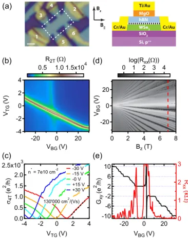
FIG. 1. Device layout and basic characterization of WSe2/graphene/h-BN vdW heterostructures. (a) An optical image of device A before the fabrication of the top gate, whose outline is indicated by the dashed white rectangle. On the right is a schematic cross section and the directions of the magnetic fields are indicated.
The scale bar is 1μm. The data in (b)–(e) are from device B. The two-terminal resistance measured from lead 1 to lead 2 is shown as a function of top and back gate voltage. A pronounced resistance maximum tunable by both gates indicates the charge neutrality point (CNP) of the bulk device, whereas a fainter line only changing with VBGindicates the CNP from the device area close to the contacts that are not covered by the top gate. (c) Cuts inVTGat differentVBGof the conductivity measured in a four-terminal configuration, which are also used to extract field effect mobility (linear fit indicated by the dashed black line) and residual doping as indicated. (d) The fan plot of longitudinal resistanceRxxversusVBGandBzatVTG= −1.42 V and (e) a cut atBz=7 T. Clear plateaus are observed at filling factors ν= ±2,±3,±4, . . ., indicating full lifting of the fourfold degeneracy of graphene for magnetic fields>6 T.
A heavily doped silicon substrate with 300 nm SiO2 was used as a global back gate. An optical image of a typical device and a cross section is shown in Fig. 1(a). In total, three different samples with a total of four devices were fabricated. Devices A, B, and C are presented in the main text and device D is discussed in the Supplemental Material [34]. Standard low-frequency lock-in techniques were used to measure two- and four-terminal conductance and resistance.
Weak antilocalization was measured at temperatures of 30 mK to 1.8 K, whereas a classical background was measured at sufficiently large temperatures of 30 to 50 K.
III. RESULTS A. Device characterization
The two-terminal resistance measured from contact 1 to contact 2 as a function of applied top and bottom gate is shown in Fig.1(b). A pronounced resistance maximum, tunable by both gates, indicates the CNP of the bulk of the device, whereas a fainter line only changing withVBGindicates the CNP from the device areas close to the contacts, which are not covered by the top gate. From the four-terminal conductivity, shown in Fig.1(c), the field effect mobilityμ1.3×105cm2V−1s−1 and the residual dopingn∗ =7×1010 cm−2 were extracted.
The mobility was extracted from a linear fit of the conductivity as a function of density at negativeVBG. At positiveVBGthe mobility is higher as one can easily see from Fig. 1(c). At VBG25 V, the lever arm of the back gate is greatly reduced since the WSe2layer gets populated with charge carriers, e.g., the Fermi level is shifted into some trap states in the WSe2. Although the WSe2is poorly conducting (low mobility), it can screen potential fluctuations due to disorder and this can lead to a larger mobility in the graphene layer, as similarly observed in graphene on MoS2[35].
Figure1(d)shows the longitudinal resistance as a function of magnetic field and gate voltage with lines originating from the integer quantum Hall effect. At low fields, the normal single-layer spectrum is obtained with plateaus at filling factors ν= ±2,±6,±10,±14, . . ., whereas at larger magnetic fields full degeneracy lifting is observed with plateaus at filling fac- torsν= ±2,±3,±4,±5,±6, . . .. The presence of symmetry- broken states, that are due to electron-electron interactions [36], is indicative of a high device quality. In the absence of interaction-driven symmetry breaking, the spin splitting of the quantum Hall states could be used to investigate the SOC strength [37].
The high quality of the devices presented here poses severe limitations on the investigation of the SOC strength using WAL theory. Ballistic transport features (transverse magnetic focusing) are observed at densities larger than 8×1011cm2. Therefore, a true diffusive regime is only obtained close to the CNP, where the charge carriers are quasidiffusive [38].
B. Magnetoconductance
In a diffusive conductor, the charge-carrier trajectories can form closed loops after several scattering events. The presence of time-reversal symmetry leads to a constructive interference of the electronic wave function along these trajectories and therefore to an enhanced backscattering probability compared to the classical case. This phenomenon is known as weak localization (WL). Considering the spin degree of freedom of the electrons, this can change. If strong SOC is present the spin can precess between scattering events, leading to destructive interference and hence to an enhanced forward- scattering probability compared to the classical case. This phenomenon is known as weak antilocalization [39]. The quantum correction to the magnetoconductivity can therefore reveal the SOC strength.
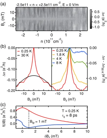
The two-terminal magnetoconductivity σ =σ(B)− σ(B=0) versusBz andn atT =0.25 K and zero perpen- dicular electric field is shown in Fig. 2(a). A clear feature
-10 0 10
Bz (mT)
-2 -1 0 1 2
n (1011cm-2) (a)
-1.0 -0.5 0.0 0.5 Δσ (e/h) 2
-2.5e11 < n < +2.5e11 cm-2, E = 0 V/m
-0.20 -0.15 -0.10 -0.05 0.00
Δσ (e2 /h)
-10 0 10
Bz (mT)
-0.10 -0.05 0.00
Δσ - Δσ30 K (e 2/h)
-10 0 10
Bz (mT) 0.25 K
30 K
0.25 K 1.8 K 4 K 8 K
(b)
0.8 0.4
42 f(δB) (e/h) 0.0
10 8 6 4 2 0
δBz (mT)
T = 0.25 K τφ = 8 ps Bip = 1 mT
(c)
FIG. 2. Magnetoconductivity of device A. (a) Magnetoconduc- tivity versusBz andnis shown at T =0.25 K. A clear feature is observed aroundB=0 mT and large modulations due to UCF are observed inBz and n. (b) Magnetoconductivity averaged over all traces at differentn. The WAL peak completely disappears atT = 30 K, leaving the classical magnetoconductivity as a background. The 30 K trace is offset vertically for clarity. The quantum correction to the magnetoconductivity is then obtained by subtracting the high- temperature background from the magnetoconductivity; see (b) on the right for different temperatures. With increasing temperature the phase coherence time shortens and therefore the WAL peak broadens and reduces in height. (c) Autocorrelation of the magnetoconductivity in red and its derivative in blue (without scale). The minimum of the derivative indicates the inflection point (Bip) of the autocorrelation, which is a measure ofτφ.
at Bz=0 mT is visible, as well as large modulations in Bzandn due to universal conductance fluctuations (UCFs).
UCFs are not averaged out since the device size is on the order of the dephasing length lφ. Therefore, an ensemble average of the magnetoconductivity over several densities is performed to reduce the amplitude of the UCFs [23], and curves as in Fig.2(b)result. A clear WAL peak is observed at 0.25 K, whereas at 30 K the quantum correction is fully suppressed due to a very short phase coherence time and only a classical background in magnetoconductivity remains.
This high-temperature background is then subtracted from the low-temperature measurements to extract the real quantum correction to the magnetoconductivity [24].
In addition to WL and WAL measurements the phase coherence time can be extracted independently from the
autocorrelation function of UCF in magnetic field [40]. UCF as a function ofBzwas measured in a range where the WAL did not contribute to the magnetoconductivity (e.g., 20–70 mT) and an average over several densities was performed. The inflection point in the autocorrelation (Bip), determined by the minimum in its derivative, is a robust measure ofτφ =2eDB3 ¯hip [41] [see Fig.2(c)].
C. Fitting
To extract the spin-orbit scattering times we use the theo- retical formula derived by diagrammatic perturbation theory [42]. In the case of graphene, the quantum correction to the magnetoconductivity σ in the presence of strong SOC is given by
σ(B)= − e2 2π h
F
τB−1 τφ−1
−F
τB−1 τφ−1+2τasy−1
−2F
τB−1 τφ−1+τasy−1+τsym−1
, (2)
where F(x)=ln(x)+(1/2+1/x), with (x) being the digamma function,τB−1=4eDB/¯h, whereDis the diffusion constant,τφis the phase coherence time,τasyis the spin-orbit scattering time due to SOC terms that are asymmetric upon z/−zinversion (HR), andτsymis the spin-orbit scattering time due to SOC terms that are symmetric uponz/−zinversion (HI, HV Z) [42]. The total spin-orbit scattering time is given by the sum of the asymmetric and symmetric rate:τSO−1 =τasy−1+τsym−1. In general, Eq. (2) is only valid if the intervalley scattering rate τiv−1 is much larger than the dephasing rateτφ−1 and the rates due to spin-orbit scattering,τasy−1andτsym−1.
In the limit of very weak asymmetric but strong symmetric SOC (τasyτφ τsym), Eq. (2) describes reduced WL since the first two terms cancel and therefore a positive magneto- conductivity results. Contrary to that, in the limit of very weak symmetric but strong asymmetric SOC (τsym τφτasy), a clear WAL peak is obtained. If both time scales are shorter than τφ, the ratioτasy/τsym will determine the quantum correction of the magnetoconductivity. In the limit of total weak SOC (τasy,τsymτφ), the normal WL in graphene is obtained [43], as the first two terms cancel and other terms explicitly involving the inter- and intravalley scattering must be considered (see the Supplemental Material [34]).
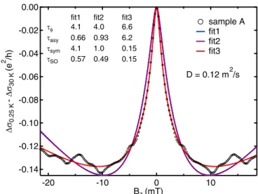
Since the second and the third terms can produce very similar dependencies on Bz it can be hard to properly dis- tinguish between the influence ofτasyandτsym onσ(B), as also previously reported [24,28]. It is therefore important to measure and fit the magnetoconductivity to sufficiently large fields in order to capture the influence of the second and third terms, which only significantly contribute at larger fields (for strong SOC). However, there is an upper limit of the field scale (the so-called transport fieldBtr) at which the theory of WAL breaks down. The size of the shortest closed loops that can be formed in a diffusive sample is on the order ofl2mfp, where lmfp is the mean-free path of the charge carriers. Fields that are larger than0/ lmfp2 , where0=h/eis the flux quantum, are not meaningful in the framework of diffusive transport.
-0.14 -0.12 -0.10 -0.08 -0.06 -0.04 -0.02 0.00
Δσ0.25 K - Δσ30 K (e2 /h)
-20 -10 0 10
Bz (mT)
sample A fit1 fit2 fit3 fit1 fit2 fit3
τφ 4.1 4.0 6.6
τasy 0.66 0.93 6.2 τsym 4.1 1.0 0.15 τSO 0.57 0.49 0.15
D = 0.12 m2/s
FIG. 3. Fitting of quantum correction to the magnetoconductivity of device A. The quantum correction to the magnetoconductivity is fit using Eq. (2). The results for three different limits are shown and their parameters are indicated (in units of picoseconds).τφis estimated to be 8 ps from the autocorrelation of UCF in the magnetic field [see Fig.2(c)].
In the most general case there are three different regimes in the presence of strong SOC in graphene:τasyτsym,τasy∼ τsym, andτasyτsym. Therefore, we fitted the magnetocon- ductivity with initial fit parameters in these three limits. An example is shown in Fig.3, where the three different fits are shown as well as the extracted parameters. Obviously, the case τasyτsym (fit 1) andτasy∼τsym(fit 2) are indistinguishable and fit the data worse than the case τasyτsym (fit 3). In addition,τφ extracted from the UCF matches best for fit 3.
Therefore, we can clearly state that the symmetric SOC is stronger than the asymmetric SOC. The flat background as well as the narrow width of the WAL peak can only be reproduced within the third case. Additionally, measurements at 1.8 K over a larger magnetic field range confirm this finding, as shown in the Supplemental Material [34].
A very similar behavior was found in device C at the CNP.
In device B (shown in the Supplemental Material), whose mobility is larger than the one from device A, we cannot clearly distinguish the three limits as the transport field is too low (≈12 mT) and the flat background at larger field cannot be used to disentangle the different parameters from each other.
However, this does not contradictτasyτsymand the overall strength of the SOC (τSO0.2 ps) is in good agreement with device A shown here.
Obviously, the extracted time scales should be taken with care as many things can introduce uncertainties in the extracted time scales. First of all, we are looking at ensemble-averaged quantities and it is clear that this might influence the precision of the extracted time scales. In addition, the subtraction of a high-temperature background can lead to higher uncertainty of the quantum correction. Lastly, the high mobility of the clean devices places severe limitations on the usable range of magnetic field. All these influences lead us to a conservative estimation of a 50% uncertainty for the extracted time scales.
Nevertheless, the order of magnitude of the extracted time scales and trends are still robust.
2.0x10¹³ 1.5
1.0
0.5 τsym-1 (s-1 )
2 1 0.67 0.5x10⁻¹³
τsym (s) 40
30 20 10 σ (e2 /h)
-10x1015-5 0 5 10 n (m-2)
45'000 cm2/(Vs)
34'000 cm2/(Vs)
CNP 3.3 5.0 -3.3x10⁻¹² cm-2 n:
15x1010 10
-1-1 τ (s)asy 5
350x10-15 300
250
200 τp (s)
2 1 0.67x10⁻¹¹
τasy (s) T = 1.8 K
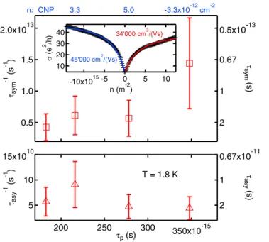
FIG. 4. Density dependence of device C. The dependence of the spin-orbit scattering ratesτsym−1 andτasy−1as a function ofτpare shown for device C. The error bars on the spin-orbit scattering rates are given by a conservative estimate of 50%. The two-terminal conductivity is shown in the inset and the extracted mobilities for thenandpside are indicated. The density of each data point is indicated in blue above the top graph. The magnetoconductivity was averaged over a density range of 3.3×1012cm−2centered around the value given at the top.
The presence of a top and a back gate allows us to tune the carrier density and the transverse electric field independently.
The spin-orbit scattering rates were found to be electric field independent at the CNP in the range of−0.05 to 0.05 V nm−1 within the precision of parameter extraction. Details are given in the Supplemental Material [34]. Within the investigated electric field range, τasy was found to be in the range of 5 to 10 ps, always close toτφ.τsym, on the other hand, was found to be around 0.1–0.3 ps whileτp was around 0.2–0.3 ps (see the Supplemental Material [34] for more details). The lack of electric field tunability ofτasy andτsym in the investigated electric field range is not so surprising. The Rashba coupling in this system is expected to change considerably for electric fields on the order of 1 V nm−1, which are much larger than the applied fields here. However, such large electric fields are hard to achieve. In addition,τsym, which results fromλI and λV Z, is not expected to change much with electric field as long as the Fermi energy is not shifted into the conduction or valence band of the WSe2 [14]. These findings contradict another study [26], which claims an electric field tunability of both SOC terms. However, there it is not discussed how accurately those parameters were extracted.
D. Density dependence
The momentum relaxation timeτpcan be tuned by changing the carrier density in graphene. Figure4shows the dependence ofτasy−1andτsym−1 onτpin device C. The lower mobility of device C allowed for WAL measurements at higher charge-carrier densities not accessible in devices A and B. At the CNP,τasy−1
10x10-12 8 6 4 2 0
τ (s)
2.5 2.0 1.5 1.0 0.5 0.0
B|| (T)
τφ
τSO
(b)
-0.10 -0.05 0.00 0.05
ΔσT=1.8 K - ΔσT=30 K (e2 /h)
-20 -10 0 10 20
Bz (mT)
B|| = 0.0 T B|| = 0.4 T B|| = 1.2 T B|| = 2.0 T B|| = 2.8 T fits
(a) B|| = 5 T
B|| = 7 T B|| = 9 T
FIG. 5. In-plane magnetic field dependence of device A. (a) The quantum correction to the magnetoconductivity at the CNP and at zero perpendicular electric field is shown for different in-plane magnetic field strengthsB. Here,nwas averaged in the range of−1×10¹¹ to 1×1011cm−2. The WAL peak gradually decreases in height and broadens asB is increased. The traces atB =5, 7, and 9 T are offset by 0.03e2/ hfor clarity. (b) The extracted phase coherence timeτφ
and the total spin-orbit scattering timeτSO are plotted versusB .τφ
clearly reduces, whereasτSOremains roughly constant over the full B range investigated. The error bars onτSO andτφ are given by a conservative estimate of 50%.
andτsym−1 are found to be consistent across all three devices A, B, and C. Here,τsym−1 increases with increasingτp, whereasτasy−1 is roughly constant with increasingτp. The dependence of the spin-orbit scattering times on the momentum scattering time can give useful insights into the dominating spin relaxation mechanisms, as discussed later. It is important to note that the extractedτasyis always very close toτφ. Therefore,τasycould be longer than the extracted value sinceτφacts as a cutoff.
E. In-plane magnetic field dependence
An in-plane magnetic field (B ) is expected to lift the influence of SOC on the quantum correction to the magne- toconductivity at sufficiently large fields. This means that a crossover from WAL to WL for z/−z asymmetric and a crossover from reduced WL to full WL correction forz/−z symmetric spin-orbit coupling is expected at a field where the Zeeman energy is much larger than the SOC strength [42]. The experimental determination of this crossover field allows for an estimate of the SOC strength.
The B dependence of the quantum correction to the magnetoconductivity of device A at the CNP and at zero perpendicular electric field was investigated, as shown in Fig.5.
The WAL peak decreases and broadens with increasingB until it completely vanishes atB 3 T. Neither a reappearance of
the WAL peak nor a transition to WL is observed at higherB fields (up to 9 T). A qualitatively similar behavior was observed for device D. Fits with Eq. (2) allow the extraction ofτφ and τSO, which are shown in Fig.5(b)forB fields lower than 3 T.
A clear decrease ofτφis observed whileτSOremains constant.
The reduction in τφ with increasing B was previously attributed to enhanced dephasing due to a random vector potential created by a corrugated graphene layer in an in-plane magnetic field [44]. The clear reduction inτφ with constant τSO and the absence of any appearance of WL at larger B also strongly suggests that a similar mechanism is at play here. Therefore, the vanishing WAL peak is due to the loss of phase coherence and not due to the fact that the Zeeman energy (Ez) is exceeding the SOC strength. Using the range where WAL is still present, we can define a lower bound of the crossover field whenτφdrops below 80% of its initial value, which corresponds to 2 T here. This leads to a lower bound of the SOC strengthλSOC Ez∼0.2 meV given agfactor of 2.
IV. DISCUSSION
The effect of SOC was investigated in high-quality vdW heterostructures of WSe2/graphene/h-BN at the CNP, as there the effects of SOC are expected to be most important. The two-terminal conductance measurements are not influenced by contact resistances or byp-ninterfaces close to the CNP due to the dominance of the intrinsic graphene resistance at the CNP.
At larger doping, the two-terminal conductance would need to be considered with care.
Phase coherence times around 4–7 ps were consistently found from fits to Eq. (2) and from the autocorrelation of UCF.
It is commonly known that the phase coherence time is shorter at the CNP than at larger doping [44,45]. Moreover, large diffusion constants lead to long phase coherence lengths being on the order of the device size (lφ=
Dτφ ≈1μm), which in turn leads to large UCF amplitudes making the analysis harder.
In general Eq. (2) is only applicable for shortτiv. Since τiv is unknown in these devices, only an estimate can be given here. WL measurements of graphene onh-BN and in fullyh-BN encapsulated graphene foundτiv on the order of picoseconds [46,47]. Intervalley scattering is only possible at sharp scattering centers as it requires a large momentum change. It is a reasonable assumption that the defect density in WSe2, which is around 1×1012 cm−2 [48], is larger than in the high-qualityh-BN [49]. This leads to shorterτiv times in graphene placed on top of WSe2and makes Eq. (2) applicable despite the short spin-orbit scattering times found here. In the case of weaker SOC, Eq. (2) cannot be used.
Instead, a more complex analysis including τiv and τ∗ is needed. This was used for device D and is presented in the Supplemental Material [34].
The following part of the discussion is dedicated to the interpretation of the extracted spin-orbit scattering time scales τasyandτsym. First, their magnitude and their relative strength are discussed. Next, the individual spin-orbit components giving rise toτsymandτasyare considered and their strengths are estimated. Finally, an overview and a possible band structure are given.
A. Spin-orbit scattering times and their anisotropy Spin-orbit scattering rates were successfully extracted at the CNP andτasy was found to be around 4–7 ps, whereas τsym was found to be much shorter, around 0.1–0.3 ps. In these systems, ifτiv is sufficiently short,τasy/2 is predicted to represent the out-of-plane spin relaxation timeτ⊥ andτSO then represents the in-plane spin relaxation timeτ [42]. For the time scales stated above, a lower bound of the spin relaxation anisotropyτ⊥/τ ∼20 is found (see the Supplemental Material [34] for detailed calculation). This large anisotropy in spin relaxation is unique for systems with a strong valley-Zeeman SOC [18]. Similar anisotropies have been found recently in spin valves in similar systems [30,31]. While the measured spin relaxation anisotropy is similar, the time scales extracted from Hanle and spin valve measurements differ by roughly one order of magnitude from the time scales extracted here.
This large discrepancy might be attributed to the different measurement techniques that could probe different time scales.
However, further theoretical and experimental work is needed to clarify this issue.
In order to link spin-orbit scattering time scales to SOC strengths, spin relaxation mechanisms have to be considered.
The simple definition of ¯h/τSOas the SOC strength is only valid in the limit where the precession frequency is much larger than the momentum relaxation rate (e.g., full spin precession occurs between scattering events). In the following we concentrate on the parameters from device A that were extracted close to the CNP. The dependence onτp in device A can most likely be assumed to be very similar to that observed in device C. Within the investigated density range of−2.5×10¹¹ to 2.5×1011 cm−2, including residual doping, an average Fermi energy of 45 meV was estimated. This is based on the density of states of pristine graphene, which should be an adequate assumption for a Fermi energy larger than any SOC strengths.
B. z→ −zsymmetric SOC (τsym)
The symmetric spin-orbit scattering time τsym contains contributions from the intrinsic SOC and from the valley- Zeeman SOC. Up to now, only the intrinsic SOC has been considered in the analysis of WAL measurements, and the impact of valley-Zeeman SOC has been ignored. However, as we now explain, it is highly unlikely that intrinsic SOC is responsible for the small values ofτsym.
In a first step, we only consider the intrinsic SOC as a source of spin relaxation. The intrinsic SOC is expected to relax spin via the Elliott-Yafet (EY) mechanism [50], which is given as
τsym,I = 2EF
λI 2
τp, (3)
whereτsym,Iis the spin relaxation time stemming from intrinsic SOC only,EF is the Fermi energy, λI is the intrinsic SOC strength, andτp is the momentum relaxation time [50]. Since the intrinsic SOC does not lead to spin-split bands and hence no spin-orbit fields exist that could lead to spin precession, a relaxation via the Dyakonov-Perel mechanism can be ex- cluded. Therefore, we can estimateλI =2EF/√
τsym,Iτp−1 ∼ 110 meV using τsym,I ∼0.2 ps, a mean Fermi energy of 45 meV, and a momentum relaxation time of 0.3 ps. The
extracted value for λI would correspond to the opening of a topological gap of 220 meV. In the presence of a small residual doping (here 30 meV), such a large topological gap should easily be detectable in transport. However, none of our transport measurements confirm this. In addition, the increase ofτsym−1 withτp, as shown in Fig.4, does not support the EY mechanism. We therefore rule out the intrinsic SOC as the dominant spin relaxation origin.
On the other hand, Cummingset al.have shown that the in-plane spins are also relaxed by the valley-Zeeman term via a Dyakonov-Perel mechanism whereτivtakes the role of the momentum relaxation time [18]:
τsym,V Z−1 = 2λV Z
¯ h
2
τiv. (4)
While this equation applies in the motional narrowing regime of spin relaxation, our measurement appears to be near the transition where that regime no longer applies. Taking this into consideration (see the Supplemental Material [34]), we estimateλV Zto be in the range of 0.23 to 2.3 meV for aτsym,V Z of 0.2 ps and a τiv of 0.1–1 ps. This agrees well with first- principles calculations [22]. The large range in λV Z comes from the fact thatτivis not exactly known.
Obviously, τsym could still contain parts that are related to the intrinsic SOC (τsym−1 =τsym,I−1 +τsym,V Z−1 ). As an upper bound ofλI, we can give a scale of 15 meV, which corresponds to half the energy scale due to the residual doping in the system.
This would lead toτsym,I ∼10 ps. Such a slow relaxation rate (τsym,I−1 ) is completely masked by the much larger relaxation rateτsym,V Z−1 coming from the valley-Zeeman term. Therefore, the presence of the valley-Zeeman term makes it very hard to give a reasonable estimate of the intrinsic SOC strength and we conclude thatτsym=τsym,V Z.
C. z→ −zasymmetric SOC (τasy)
The asymmetric spin-orbit scattering time τasy contains contributions from the Rashba SOC and from the PIA SOC.
Since the PIA SOC scales linearly with the momentum, it can be neglected at the CNP. Here,τasy represents only the spin-orbit scattering time coming from Rashba SOC. It is known that Rashba SOC can relax the spins via the Elliott-Yafet mechanism [50]. In addition, the Rashba SOC leads to a spin splitting of the bands and therefore to a spin-orbit field. This opens a second relaxation channel via the Dyakonov-Perel (DP) mechanism [51]. In principle the dependence on the mo- mentum scattering timeτp allows one to distinguish between these two mechanisms. Here, τasy−1 does not monotonically depend onτpas one can see in Fig.4and therefore we cannot unambiguously decide between the two mechanisms.
Assuming that only the EY mechanism is responsible for spin relaxation, then λR =EF/√
4τasyτp−1∼5.0 meV can be estimated, using τasy of 6 ps, a mean Fermi energy of 45 meV, and a momentum relaxation time of 0.3 ps. On the other hand, pure DP-mediated spin relaxation leads to λR =h/¯
2τasyτp ∼0.35 meV. The Rashba SOC strength estimated by the EY relaxation mechanism is large compared to first-principles calculations [22], which agree much better
-40 -20 0 20 40
E (meV)
-100 -50 0 50 100
|k| (106 m-1) (a) Δ = 0.54 meV
λI = 0.06 meV λVZ = 1 meV λR = 0.35 meV
-6 -4 -2 0 2 4 6
E (meV)
-10 -5 0 5 10
|k| (106 m-1) (b)
~ 2 λVZ
8 4 0 -4 -8
E (meV)
-10 -5 0 5 10
|k| (106 m-1) (c)
λI = 5 meV
FIG. 6. Possible low-energy band structures: (a), (b) band struc- tures using the Hamiltonian of Eq. (1) with the parameters listed in (a). The unknown parametersandλIwere taken from Ref. [22]. In (a), the band structure is shown in the density range of−2.5×10¹¹ to 2.5×1011cm−2 (CNP), which corresponds the one investigated above. The energy range dominated by charge puddles is indicated by the grey shaded region. (b) Zoom-in at low energy. (c)λIof 5 meV is assumed to show the changes due to the unknownλIat low energy.
with the SOC strength estimated by the DP mechanism. This is also in agreement with previous findings [25,27].
D. Band-structure analysis
Since there is a finite valley-Zeeman SOC, which is a result of different intrinsic SOC on the A sublattice and B sublattice, a staggered sublattice potential can also be expected. The presence of a staggered potential, meaning that the on-site energy of the A atom is different from the B atom on average, leads to the opening of a trivial gap ofat the CNP. Since there is no evidence of an orbital gap, we take the first-principles calculations as an estimate of=0.54 meV.
Knowing all relevant parameters in Eq. (1), a band structure can be calculated, which is shown in Fig.6. The bands are spin split mainly due to the presence of strong valley-Zeeman SOC but also due to the weaker Rashba SOC. At very low energies, an inverted band is formed due to the interplay of the valley-Zeeman and Rashba SOC [see Fig.6(b)]. This system was predicted to host helical edge states for zigzag graphene nanoribbons, demonstrating the quantum spin Hall effect [22].
In the case of stronger intrinsic SOC, which we cannot estimate accurately, a band structure as in Fig.6(c)is expected with a topological gap appearing at low energies. We would like to note here that this system might host a quantum spin Hall phase.
However, its detection is still masked by device quality as the minimal Fermi energy is much larger than the topological gap [see also Fig.6(a)].
Our findings are in good agreement with the calculations by Gmitraet al.[22]. However, we have to remark that whereas the calculations were performed for single-layer TMDCs, we have used multilayer WSe2as a substrate. Single-layer TMDCs are direct band-gap semiconductors with the band gap located at theK-point, whereas multilayer TMDCs have an indirect band gap. Since the SOC results from the mixing of the graphene orbitals with the WSe2 orbitals, the strength of the induced SOC depends on the relative band alignment between the graphene and WSe2band, which will be different for single- or multilayer TMDCs. This difference was recently shown by Wakamuraet al.[28]. Therefore, using single-layer WSe2to induce SOC might even enhance the coupling found by our study. Furthermore, the parameters taken from Ref. [22] for the orbital gap and for the intrinsic SOC have to be taken with care.
V. CONCLUSION
In conclusion we measured weak antilocalization in high- quality WSe2/graphene/h-BN vdW heterostructures at the charge-neutrality point. The presence of a clear WAL peak reveals a strong SOC. Whereas previous studies have also found a clear WAL signal, we present a complete interpre- tation of all involved SOC terms considering their relaxation mechanisms. This includes the finding of a very large spin relaxation anisotropy that is governed by the presence of a valley-Zeeman SOC that couples spin to valley. The relaxation mechanism at play here is very special since it relies on intervalley scattering and can only occur in materials where a valley degree of freedom is present and coupled to spin. This is in good agreement with recent spin-valve measurements that found also very large spin relaxation anisotropies in similar systems [30,31].
In addition, we investigated the influence of an in-plane magnetic field on the WAL signature. Due to the loss of phase coherence, a lower bound of all SOC strengths of 0.2 meV can
be given, which is in agreement with the numbers presented above. This approach does not depend on the accurate fit- ting of WAL peaks or on the interpretation of the extracted spin-orbit scattering rates and is therefore a very robust method.
The coupling of spin and valley opens new possibilities in exploring spin and valley degrees of freedom in graphene. In the case of bilayer graphene in proximity to WSe2an enormous gate tunability of the SOC strength is predicted since full layer polarization can be achieved by an external electric field [19,20]. This is just one of many possible routes for future investigations.
ACKNOWLEDGMENTS
The authors gratefully acknowledge fruitful discussions on the interpretation of the experimental data with Martin Gmitra and Vladimir Fal’ko. Clevin Handschin is acknowledged for helpful discussions on the sample fabrication. This work has received funding from the European Union’s Horizon 2020 research and innovation program under Grant No. 696656 (Graphene Flagship), the Swiss National Science Foundation, the Swiss Nanoscience Institute, the Swiss NCCR QSIT, ISpinText FlagERA network, the OTKA PD-121052, OTKA FK-123894, and OTKA K112918. P.M. acknowledges support from the Bolyai Fellowship. ICN2 is supported by the Severo Ochoa program from Spanish MINECO (Grant No. SEV-2013- 0295) and funded by the CERCA Programme/Generalitat de Catalunya. K.W. and T.T. acknowledge support from the Elemental Strategy Initiative conducted by the MEXT, Japan, and JSPS KAKENHI Grant No. JP15K21722.
S.Z. fabricated and measured the devices with the help of P.M. K.M. contributed to the fabrication of device C. S.Z.
anayzed the data with help from P.M. and inputs from C.S..
S.Z., P.M., A.W.C., J.H.G., and C.S. were involved in the interpretation of the results. S.Z. wrote the manuscript with inputs from P.M., C.S., A.W.C., and J.H.G. K.W. and T.T.
provided theh-BN crystals used in the devices.
[1] A. K. Geim and I. V. Grigorieva, Van der Waals heterostructures, Nature (London)499,419(2013).
[2] L. A. Ponomarenko, R. V. Gorbachev, G. L. Yu, D. C. Elias, R.
Jalil, A. A. Patel, A. Mishchenko, A. S. Mayorov, C. R. Woods, J. R. Wallbank, M. Mucha-Kruczynski, B. A. Piot, M. Potemski, I. V. Grigorieva, K. S. Novoselov, F. Guinea, V. I. Fal’ko, and A.
K. Geim, Cloning of Dirac fermions in graphene superlattices, Nature (London)497,594(2013).
[3] C. R. Dean, L. Wang, P. Maher, C. Forsythe, F. Ghahari, Y. Gao, J. Katoch, M. Ishigami, P. Moon, M. Koshino, T.
Taniguchi, K. Watanabe, K. L. Shepard, J. Hone, and P. Kim, Hofstadter’s butterfly and the fractal quantum Hall effect in Moiré superlattices,Nature (London)497,598(2013).
[4] B. Hunt, J. D. Sanchez-Yamagishi, A. F. Young, M. Yankowitz, B. J. LeRoy, K. Watanabe, T. Taniguchi, P. Moon, M. Koshino, P.
Jarillo-Herrero, and R. C. Ashoori, Massive Dirac fermions and Hofstadter butterfly in a van der Waals heterostructure,Science 340,1427(2013).
[5] M. Lee, J. R. Wallbank, P. Gallagher, K. Watanabe, T. Taniguchi, V. I. Fal’ko, and D. Goldhaber-Gordon, Ballistic miniband conduction in a graphene superlattice,Science353,1526(2016).
[6] Z. Wang, C. Tang, R. Sachs, Y. Barlas, and J. Shi, Proximity- Induced Ferromagnetism in Graphene Revealed by the Anoma- lous Hall Effect,Phys. Rev. Lett.114,016603(2015).
[7] J. C. Leutenantsmeyer, A. A. Kaverzin, M. Wojtaszek, and B. J.
van Wees, Proximity induced room temperature ferromagnetism in graphene probed with spin currents, 2D Mater.4, 014001 (2017).
[8] D. K. Efetov, L. Wang, C. Handschin, K. B. Efetov, J. Shuang, R. Cava, T. Taniguchi, K. Watanabe, J. Hone, C. R. Dean, and P. Kim, Specular interband Andreev reflections at van der Waals interfaces between graphene and NbSe2, Nat. Phys.12, 328 (2015).
[9] L. Bretheau, J. I.-J. Wang, R. Pisoni, K. Watanabe, T. Taniguchi, and P. Jarillo-Herrero, Tunnelling spectroscopy of Andreev states in graphene,Nat. Phys.13,756(2017).
[10] C. L. Kane and E. J. Mele, Quantum Spin Hall Effect in Graphene,Phys. Rev. Lett.95,226801(2005).
[11] S. Konschuh, M. Gmitra, and J. Fabian, Tight-binding theory of the spin-orbit coupling in graphene,Phys. Rev. B82,245412 (2010).
[12] A. H. Castro Neto and F. Guinea, Impurity-Induced Spin-Orbit Coupling in Graphene,Phys. Rev. Lett.103,026804(2009).
[13] W. Han, R. K. Kawakami, M. Gmitra, and J. Fabian, Graphene spintronics,Nat. Nanotechnol.9,794(2014).
[14] M. Gmitra and J. Fabian, Graphene on transition-metal dichalco- genides: A platform for proximity spin-orbit physics and op- tospintronics,Phys. Rev. B92,155403(2015).
[15] M. Drögeler, C. Franzen, F. Volmer, T. Pohlmann, L. Banszerus, M. Wolter, K. Watanabe, T. Taniguchi, C. Stampfer, and B.
Beschoten, Spin lifetimes exceeding 12 ns in graphene nonlocal spin valve devices,Nano Lett.16,3533(2016).
[16] S. Singh, J. Katoch, J. Xu, C. Tan, T. Zhu, W. Amamou, J. Hone, and R. Kawakami, Nanosecond spin relaxation times in single layer graphene spin valves with hexagonal boron nitride tunnel barriers,Appl. Phys. Lett.109,122411(2016).
[17] J. Ingla-Aynés, M. H. D. Guimarães, R. J. Meijerink, P. J. Zomer, and B. J. van Wees, 24-μm spin relaxation length in boron nitride encapsulated bilayer graphene,Phys. Rev. B92,201410 (2015).
[18] A. W. Cummings, J. H. Garcia, J. Fabian, and S. Roche, Giant Spin Lifetime Anisotropy in Graphene Induced by Proximity Effects,Phys. Rev. Lett.119,206601(2017).
[19] M. Gmitra and J. Fabian, Proximity Effects in Bilayer Graphene on Monolayer WSe2: Field-Effect Spin Valley Locking, Spin- Orbit Valve, and Spin Transistor,Phys. Rev. Lett.119,146401 (2017).
[20] J. Y. Khoo, A. F. Morpurgo, and L. Levitov, On-Demand Spin-Orbit Interaction from Which-Layer Tunability in Bilayer Graphene,Nano Lett.17,7003(2017).
[21] J. H. Garcia, A. W. Cummings, and S. Roche, Spin Hall effect and weak antilocalization in graphene/transition metal dichalcogenide heterostructures,Nano Lett.17,5078(2017).
[22] M. Gmitra, D. Kochan, P. Högl, and J. Fabian, Trivial and inverted Dirac bands and the emergence of quantum spin Hall states in graphene on transition-metal dichalcogenides,Phys.
Rev. B93,155104(2016).
[23] Z. Wang, D.-K. Ki, H. Chen, H. Berger, A. H. MacDonald, and A. F. Morpurgo, Strong interface-induced spin-orbit interaction in graphene on WS2,Nat. Commun.6,8339(2015).
[24] Z. Wang, D.-K. Ki, J. Y. Khoo, D. Mauro, H. Berger, L. S.
Levitov, and A. F. Morpurgo, Origin and Magnitude of “De- signer” Spin-Orbit Interaction in Graphene on Semiconducting Transition Metal Dichalcogenides, Phys. Rev. X 6, 041020 (2016).
[25] B. Yang, M.-F. Tu, J. Kim, Y. Wu, H. Wang, J. Alicea, R. Wu, M.
Bockrath, and J. Shi, Tunable spin-orbit coupling and symmetry- protected edge states in graphene/WS2, 2D Mater.3,031012 (2016).
[26] T. Völkl, T. Rockinger, M. Drienovsky, K. Watanabe, T.
Taniguchi, D. Weiss, and J. Eroms, Magnetotransport in het- erostructures of transition metal dichalcogenides and graphene, Phys. Rev. B96,125405(2017).
[27] B. Yang, M. Lohmann, D. Barroso, I. Liao, Z. Lin, Y. Liu, L.
Bartels, K. Watanabe, T. Taniguchi, and J. Shi, Strong
electron-hole symmetric Rashba spin-orbit coupling in graphene/monolayer transition metal dichalcogenide het- erostructures,Phys. Rev. B96,041409(2017).
[28] T. Wakamura, F. Reale, P. Palczynski, S. Guéron, C. Mattevi, and H. Bouchiat, Strong spin-orbit interaction induced in graphene by monolayer WS2,arXiv:1710.07483.
[29] D. Kochan, S. Irmer, and J. Fabian, Model spin-orbit coupling Hamiltonians for graphene systems,Phys. Rev. B95,165415 (2017).
[30] T. S. Ghiasi, J. Ingla-Aynés, A. A. Kaverzin, and B. J. van Wees, Large proximity-induced spin lifetime anisotropy in transition- metal dichalcogenide/graphene heterostructures,Nano Lett.17, 7528(2017).
[31] L. A. Benítez, J. F. Sierra, W. S. Torres, A. Arrighi, F. Bonell, M. V. Costache, and S. O. Valenzuela, Strongly anisotropic spin relaxation in graphene/WS2van der Waals heterostructures, Nat. Phys.(2017), doi:10.1038/s41567-017-0019-2.
[32] P. J. Zomer, M. H. D. Guimarães, J. C. Brant, N. Tombros, and B. J. van Wees, Fast pick up technique for high quality het- erostructures of bilayer graphene and hexagonal boron nitride, Appl. Phys. Lett.105,013101(2014).
[33] L. Wang, I. Meric, P. Y. Huang, Q. Gao, Y. Gao, H. Tran, T.
Taniguchi, K. Watanabe, L. M. Campos, D. A. Muller, J. Guo, P.
Kim, J. Hone, K. L. Shepard, and C. R. Dean, One-dimensional electrical contact to a two-dimensional material,Science342, 614(2013).
[34] See Supplemental Material athttp://link.aps.org/supplemental/
10.1103/PhysRevB.97.075434for details of device fabrication and measurement, additional data, including further devices, and an estimate of the valley-Zeeman SOC and the spin relaxation anisotropy.
[35] L. Basnzerus, K. Watanabe, T. Taniguchi, B. Beschoten, and C. Stampfer, Dry transfer of CVD graphene using MoS2-based stamps, Phys. Status Solidi RRL 11, 1700136 (2017).
[36] A. F. Young, C. R. Dean, L. Wang, H. Ren, P. Cadden-Zimansky, K. Watanabe, T. Taniguchi, J. Hone, K. L. Shepard, and P.
Kim, Spin and valley quantum Hall ferromagnetism in graphene, Nat. Phys.8,550(2012).
[37] T. P. Cysne, T. G. Rappoport, J. H. Garcia, and A. R. Rocha, Quantum Hall effect in graphene with interface-induced spin- orbit coupling,Phys. Rev. B97,085413(2018).
[38] S. Das Sarma, S. Adam, E. H. Hwang, and E. Rossi, Electronic transport in two-dimensional graphene,Rev. Mod. Phys.83,407 (2011).
[39] G. Bergmann, Weak anti-localization—An experimental proof for the destructive interference of rotated spin 1/2,Solid State Commun.42,815(1982).
[40] P. A. Lee, A. D. Stone, and H. Fukuyama, Universal conductance fluctuations in metals: Effects of finite temperature, interactions, and magnetic field,Phys. Rev. B35,1039(1987).
[41] M. B. Lundeberg, J. Renard, and J. A. Folk, Conductance fluctuations in quasi-two-dimensional systems: A practical view, Phys. Rev. B86,205413(2012).
[42] E. McCann and V. I. Fal’ko,z→ −zSymmetry of Spin-Orbit Coupling and Weak Localization in Graphene,Phys. Rev. Lett.
108,166606(2012).
[43] E. McCann, K. Kechedzhi, V. I. Fal’ko, H. Suzuura, T. Ando, and B. L. Altshuler, Weak-Localization Magnetoresistance and
Valley Symmetry in Graphene, Phys. Rev. Lett. 97, 146805 (2006).
[44] M. B. Lundeberg and J. A. Folk, Rippled Graphene in an In-Plane Magnetic Field: Effects of a Random Vector Potential,Phys. Rev.
Lett.105,146804(2010).
[45] F. V. Tikhonenko, D. W. Horsell, R. V. Gorbachev, and A. K.
Savchenko, Weak Localization in Graphene Flakes,Phys. Rev.
Lett.100,056802(2008).
[46] WL measurements in additionalh-BN/graphene/h-BN devices prepared in our laboratory revealed intervalley scattering times on the order of picoseconds.
[47] N. J. G. Couto, D. Costanzo, S. Engels, D.-K. Ki, K. Watanabe, T. Taniguchi, C. Stampfer, F. Guinea, and A. F. Morpurgo, Random Strain Fluctuations as Dominant Disorder Source for
High-Quality On-Substrate Graphene Devices,Phys. Rev. X4, 041019(2014).
[48] R. Addou and R. M. Wallace, Surface analysis of WSe2crystals:
Spatial and electronic variability,ACS Appl. Mater. Interfaces 8,26400(2016).
[49] T. Taniguchi and K. Watanabe, Synthesis of high-purity boron nitride single crystals under high pressure by using Ba–BN solvent,J. Cryst. Growth303,525(2007).
[50] H. Ochoa, A. H. Castro Neto, and F. Guinea, Elliot-Yafet Mechanism in Graphene, Phys. Rev. Lett. 108, 206808 (2012).
[51] M. I. Dyakonov and V. I. Perel, Spin relaxation of conduction electrons in noncentrosymmetric semiconductors, Sov. Phys.
Solid State13, 3023 (1972).