Spin transport in two-layer-CVD-hBN/graphene/hBN heterostructures
M. Gurram,1,*S. Omar,1S. Zihlmann,2P. Makk,2Q. C. Li,3Y. F. Zhang,3C. Schönenberger,2and B. J. van Wees1
1Physics of Nanodevices, Zernike Institute for Advanced Materials, University of Groningen, Nijenborgh 4, 9747 AG Groningen, The Netherlands
2Department of Physics, University of Basel, Klingelbergstrasse 82, CH-4056 Basel, Switzerland
3Center for Nanochemistry (CNC), Department of Materials Science and Engineering, College of Engineering, Peking University, 100871 Beijing, People’s Republic of China
(Received 24 October 2017; published 9 January 2018)
We study room-temperature spin transport in graphene devices encapsulated between a layer-by-layer-stacked two-layer-thick chemical vapor deposition (CVD) grown hexagonal boron nitride (hBN) tunnel barrier, and a few-layer-thick exfoliated-hBN substrate. We find mobilities and spin-relaxation times comparable to that of SiO2 substrate-based graphene devices, and we obtain a similar order of magnitude of spin relaxation rates for both the Elliott-Yafet and D’Yakonov-Perel’ mechanisms. The behavior of ferromagnet/two-layer-CVD- hBN/graphene/hBN contacts ranges from transparent to tunneling due to inhomogeneities in the CVD-hBN barriers. Surprisingly, we find both positive and negative spin polarizations for high-resistance two-layer-CVD- hBN barrier contacts with respect to the low-resistance contacts. Furthermore, we find that the differential spin- injection polarization of the high-resistance contacts can be modulated by dc bias from−0.3 to+0.3 V with no change in its sign, while its magnitude increases at higher negative bias. These features point to the distinctive spin-injection nature of the two-layer-CVD-hBN compared to the bilayer-exfoliated-hBN tunnel barriers.
DOI:10.1103/PhysRevB.97.045411 I. INTRODUCTION
Two-dimensional (2D) van der Waals heterostructures of graphene and hexagonal boron nitride (hBN) have gained a lot of attention for charge [1–3] and spin [4–7] transport studies in high electronic quality graphene. An atomically flat and dangling-bond-free hBN dielectric provides a neu- tral environment to probe the intrinsic transport properties of graphene. High-mobility graphene encapsulated between two thick-exfoliated-hBN dielectrics resulted in a large spin- relaxation length up to 24μm with spin diffusion [6], and up to 90μm with spin drift [8]. However, an efficient injection of spin-polarized current into graphene is challenging with the conventional oxide tunnel barriers, which suffer from pinholes and inhomogeneous growth [9,10] and result in irreproducible and low-spin-injection polarizations [9,11]. Recent progress in exploring different 2D materials revealed that the atomically thin, insulating, and pinhole-free nature of single-crystalline hBN makes it a promising tunnel barrier [12] for electrical spin injection and detection in graphene [13].
Combining high-mobility graphene with an exfoliated- hBN tunnel barrier resulted in a uniform mobility and spin- relaxation length across different regions of the encapsu- lated graphene [14]. Furthermore, a fully hBN-encapsulated monolayer-graphene with exfoliated-hBN tunnel barriers showed differential spin polarizations of 1–2 % with monolayer-hBN contacts [13–16], up to 100% with bilayer- hBN contacts [16], and up to 6% with trilayer-hBN contacts [17]. Thicknesses of more than three layers are not suitable for
*Author to whom all correspondence should be addressed:
m.gurram@rug.nl
spin injection [15,17,18] due to very high tunneling interface resistance. However, for large-scale spintronics applications, it is important to incorporate large-area chemical vapor de- position (CVD) grown hBN tunnel barriers in spin valves [18–21] and magnetic tunnel junctions [22,23]. Therefore, it is interesting to combine high-mobility graphene with the efficient CVD-hBN tunnel barriers for spintronics devices.
The potential of CVD-hBN as a tunnel barrier for elec- trical spin injection into graphene has been recently explored [18–21]. Electrical injection of spin current using a monolayer- CVD-hBN tunnel barrier is inefficient [18,19,21] due to its low contact resistance-area productRcA leading to the spin conductivity mismatch problem [24]. This can be overcome by increasing the number of layers, which would increase the RcAvalue leading to an efficient injection of spin current. In addition, the spin-injection efficiency is expected to be higher for a bilayer hBN barrier than for a single-layer hBN barrier [25]. However, practically, controlled and direct growth of bilayer or multilayer (>1 layer) CVD-hBN is difficult [26].
Therefore, for our samples, we prepare a two-layer-CVD-hBN tunnel barrier via layer-by-layer stacking of two individual monolayers of CVD-hBN. Note that this two-layer-CVD-hBN is different from the bilayer-CVD-hBN in that the former is layer-by-layer-stacked using two individual monolayers while the latter is as-grown.
Furthermore, previously reported spin-transport studies in graphene with CVD-hBN tunnel barriers incorporated a bare SiO2/Si substrate [18–21]. Even though hBN substrates have not been reported to enhance the spin-relaxation times of graphene compared to the SiO2/Si substrate [4], it can increase the mobility and thus the carrier diffusion.
Therefore, here we combine few-layer exfoliated-hBN as a substrate and two-layer-CVD-hBN as a tunnel barrier to obtain
TABLE I. Summary of the characteristics of the three devices. The number of layers of graphene is denoted by 1Lfor monolayer and 3L for trilayer. The source of the CVD-hBN tunnel barrier is denoted by GSM for Graphene Supermarket, Inc. The rest of the symbols have the same meaning as in the text.
CVD-hBN RcA Rsq μ Dc Ds τs Rc
Rs
L λs
Device Graphene source (k μm2) (k) (cm2V−1s−1) (m2s−1) (m2s−1) (ps)
Dev1 1L GSM 1.7–10.8 0.7–4.2 3400 0.01–0.03 0.01–0.03 343–404 0.81–12.97 0.61–1.14
Dev2 1L GSM 0.5–1.2 1.7–2.8 90 0.01–0.02 79–162 0.12–3.11 0.15–2.65
Dev3 3L in-house [27] 1.4–8.6 0.3–0.5 255 0.06–0.07 0.01–0.02 96–105 13.64–77.81 0.84–1.19
both high mobilities and high spin polarizations. The mobility of graphene is surprisingly below 3400 cm2V−1s−1, and spin relaxation time is lower than 400 ps. In contrast to the results by Kamalakaret al.[21], we observe both positive and negative spin polarizations for high-RcAcontacts with respect to the low-RcAcontacts.
We have a similar system to that reported by Gurramet al.
[16], wherein the observed behavior of bias-dependent differ- ential spin-injection polarizationpin is unique to the bilayer nature of the hBN barrier. Our system is distinctively different from the exfoliated-bilayer-hBN tunnel barrier as it consists of two individually stacked CVD hBN monolayers. This allows us to investigate whether the spin-injection efficiency depends only on the barrier thickness or also on different parameters such as relative crystallographic orientation or the quality of the interfaces. Therefore, we also studied the bias-dependent pin for high-RcA contacts, and we found that the behavior of pin for two-layer-CVD-hBN is different from that of the bilayer-exfoliated-hBN barrier in two ways. First, there is no change in sign of pin close to zero bias, and the sign does not change within the applied dc bias range of±0.3 V.
Second, the magnitude ofpinincreases only at higher negative bias. Our results represent progress in attaining promising two-layer-CVD-hBN tunnel barriers, but they point to the utmost importance of the transfer process.
II. DEVICE FABRICATION
We have prepared three devices, labeled Dev1, Dev2, and Dev3 (see TableIfor a summary of their characteristics). The devices have similar geometry, which is shown in Fig.1(a).
CVD-hBN for Dev1 and Dev2 is obtained from Graphene Supermarket, Inc. and for Dev3 it is grown in-house by two of the authors [27]. Moreover, Dev1 and Dev2 consist of monolayer-exfoliated-graphene, while Dev3 consists of trilayer-exfoliated-graphene.
The device fabrication is done in two stages. First, the stack of graphene/bottom-hBN on a SiO2/Si substrate is prepared using the dry pick-up and transfer method [28]. Then the two- layer-CVD-hBN tunnel barrier is transferred on top of the stack via the conventional wet transfer method [29].
In the first stage, we prepared a graphene/bottom-hBN stack on a SiO2/Si substrate. The flakes of graphene and bottom-hBN (typically≈10−15 nm thick) substrate were exfoliated from highly oriented pyrolytic graphite (HOPG, SPI Supplies, ZYA grade) and hBN-powder (HQ graphene), respectively, on top of a precleaned SiO2(300 nm)/Si substrate using the conventional scotch tape method [30]. The required flakes were identified via an optical microscope and atomic force microscopy. To make
the graphene/bottom-hBN stack, we followed the dry pick-up procedure described in Refs. [28] and [14]. In short, we used a glass substrate supporting a polydimethylsiloxane (PDMS) stamp prepared with a polycarbonate (PC) layer to pick up a graphene flake. Then, the PC/graphene stack is released onto a thick bottom-hBN on a SiO2(300 nm)/Si substrate by melting the PC layer. The PC layer is dissolved in chloroform for 5 h at room temperature. To remove the PC residues from the pickup and transfer process, the stacks were annealed in an Ar/H2
atmosphere at 350◦C for 12 h.
In the second stage, we first prepared the two-layer-CVD- hBN from two individual monolayers of CVD-hBN. This is achieved as follows. We start with monolayer-CVD-hBN, grown on both sides of a copper (Cu) foil. We spin-coat PMMA on one side of the Cu foil to protect the CVD-hBN layer and use physical dry etching (O2 plasma) to remove
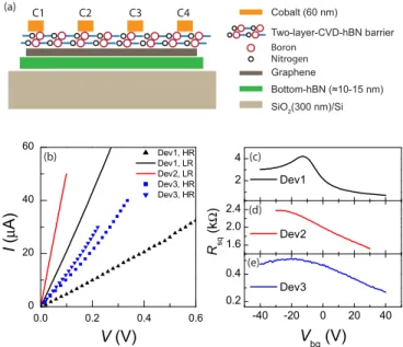
FIG. 1. (a) Schematic of the devices prepared with two-layer- CVD-hBN tunnel barriers. A slight displacement in the vertical posi- tion of the boron and nitrogen atoms of the tunnel barrier represents a crystallographic misalignment between the two CVD-hBN layers.
C1–C4 denote the contacts used for the measurements. Other contacts are not shown. (b) Representative three-terminalI-Vcurves for three devices, labeled Dev1, Dev2, and Dev3. High-resistance (HR) and low-resistance (LR) contacts are denoted in the legend with symbols and solid-line data, respectively. Within Dev2, all contacts show similar LR behavior to that of shown here. Parts (c), (d), and (e) show the square resistanceRsq of the graphene channel as a function of backgate voltageVbgfor devices Dev1, Dev2, and Dev3, respectively.
the CVD-hBN on the other side. We then use chemical wet etching to remove the copper by floating the structure PMMA/CVD-hBN/Cu in contact with ammonium persulfate (NH4)2S2O4etchant solution for 12 h. While the PMMA/CVD- hBN is still floating, the etchant is replaced with deionized (DI) water several times to clean the etchant liquid from the contact area of the PMMA/CVD-hBN. Then we transfer the cleaned PMMA/CVD-hBN on top of another as-obtained CVD-hBN/Cu/CVD-hBN foil to get the two layers of CVD- hBN on one side of the Cu foil.
The resulting two-layer-CVD-hBN/Cu/CVD-hBN struc- ture is etched following the same process as before. While the PMMA/two-layer-CVD-hBN is still floating on DI water, we transfer it onto the already prepared graphene/bottom-hBN stack on a SiO2/Si substrate. Then the final stack is put on a hotplate at 180◦C for 2 min to remove the remaining water.
Since the PMMA on top is too thick for lithography, we dis- solve it in acetone at 40◦C for 10 min. The resulting two-layer- CVD-hBN/graphene/bottom-hBN device is annealed again in an Ar/H2atmosphere to remove any PMMA residues leftover on the topmost layer.
The electrodes were patterned on the PMMA spin-coated stack using electron beam lithography, followed by deposition of ferromagnetic cobalt (Co, 60 nm) capped with aluminum (Al, 5 nm) using electron beam evaporation, and liftoff in acetone at 40◦C for 10 min. A schematic of the final device is depicted in Fig.1(a).
Note that the layer-by-layer-stacking of two individual monolayers of CVD-hBN does not guarantee a crystallo- graphic alignment between the monolayers. The misalignment between the two CVD-hBN layers is schematically represented by a slight displacement in the vertical position of the atoms in Fig.1(a).
III. RESULTS
The electrical characterization of the devices is done using a low-frequency lock-in detection technique. All the measure- ments were carried out at room temperature under vacuum conditions.
The contact resistance of the ferromagnetic tunneling con- tacts plays a crucial role in determining its spin injection and detection efficiencies [16,21]. Therefore, we have char- acterized the contacts using the three-terminal measurement scheme. The three-terminal current-voltage (I-V) characteris- tics of contacts from three devices are shown in Fig.1(b).
The differential contact resistance-area product,RcA, of the contacts measured from the three-terminal scheme at zero bias is found to be in the range 1.0–10.8 k μm2. In the literature [12,14,16,18,19], the reported values ofRcAfor monolayer- hBN fall below 4.0 k μm2, and for bilayer-hBN they fall above 4.0 k μm2. Based on these values ofRcA, we divide all the contacts of the three devices into two categories, namely high-resistance (HR,>4.0 k μm2) and low-resistance (LR, 4.0 k μm2) contacts. Accordingly, Dev1 and Dev3 show contacts ranging from LR to HR, and Dev2 shows only LR contacts. LR (HR) contacts of all devices showed linear (nonlinear)I-Vbehavior [Fig.1(b)], which is probably due to the transparent (tunneling) nature of the two-layer-CVD-hBN barriers.
The spread in theRcAvalues could be due to the inhomo- geneous growth of CVD-hBN, thickness variation from the wrinkles at the interfaces of two-layer-CVD-hBN/graphene and monolayer-CVD-hBN/monolayer-CVD-hBN during two separate wet transfer processes, and PMMA residues at the interfaces of cobalt/two-layer-CVD-hBN and monolayer- CVD-hBN/monolayer-CVD-hBN. The low-resistance of the contacts even with two layers of CVD-hBN can be attributed to the presence of pinholes coming from the inhomogeneous coverage of CVD-hBN, and cracks in CVD-hBN that might be induced during the transfer processes or the annealing step.
We use a four-terminal local measurement scheme to characterize the charge transport in graphene, where we apply a constant magnitude of ac currenti across the outer electrodes [C1 and C4 in Fig.1(a)] and measure the voltage dropvacross the inner electrodes (C2 and C3) while sweeping the backgate voltageVbg. Here, the highlyp-doped Si is used as a backgate electrode. The backgate bias Vbg dependence of the square resistanceRsq= viWL of the graphene in three devices is shown in Figs.1(c)–1(e), whereW andLare the width and length of the graphene transport channel. Typical values ofRsqwere observed for monolayer graphene in Dev1 and Dev2, whereas a very lowRsq for Dev3 is due to the trilayer nature of its graphene (see TableI). The field-effect mobility of electrons is obtained by fitting theRsq data using the relationRsq=neμ1+σ0 +ρs, withnthe carrier density,ethe electron charge,μthe mobility,σ0 the residual conductivity, andρs the contribution from short-range scattering [14,31].
The fitting resulted in surprisingly low electron mobilities μ=3400 cm2V−1s−1 for Dev1, 90 cm2V−1s−1 for Dev2, and 255 cm2V−1s−1 for Dev3. It should be noted that the bottom layers of few-layer-thick graphene could screen the gate-induced electric field. However, it was reported that for multilayer graphene up to five layers, the bulk carrier density determined from the Hall measurements agrees approximately with the backgate-induced carrier density [32]. Therefore, we assume that the obtained value of the field-effect mobility of trilayer graphene in Dev3 is correct.
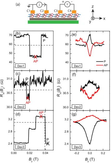
We use the four-terminal nonlocal measurement scheme [10,14] shown in Fig. 2(a)to characterize the spin transport in graphene. A spin-polarized current is injected across a pair of injector contacts [C1 and C2 in Fig. 2(a)] with a constant magnitude of the ac current i=1 μA, and the diffused spins along the graphene channel are probed as a voltagev across different pairs of detector contacts [C3 and C4 in Fig.2(a)], located outside the charge-current path. The nonlocal differential resistance is given byRnl= vi.
For a clear interpretation of the results presented here, we give RcA values of the (inner) injector–(inner) detector contacts pair [C2–C3 in Fig.2(a)]. Dev1 consists of contacts whoseRcAvalues are 1.7–10.8 k μm2(LR-HR), Dev2 with 1.2–1.0 k μm2(LR-LR), and Dev3 has two sets of contacts, namely set1 with 4.7–1.4 k μm2 (HR-LR) and set2 with 8.6–2.3 k μm2(HR-LR).
For nonlocal spin-valve measurements, a magnetic fieldBy is swept along the easy axes of the Co contacts. Magneti- zation switching of the contacts at their respective coercive fields results in sharp changes in the nonlocal differential resistance Rnl(By) value as shown in Figs. 2(b)–2(d). The injector-detector pair of Dev1 consisting of LR-HR contacts
(a)
x z yx
0.00 0.02 0.04
2.4 2.8 3.2
AP
X
P Dev3 X
Rnl(By) (Ω)
By (T)
30.0 30.5
31.0 P
X
Dev2
X
AP 40
50 60 70
P
X
X
AP Dev1
(f) (e)
(d) (c) (b)
-0.2 0.0 0.2
2.4 2.8 3.2
Dev3
(g) Rnl(Bz) (Ω)
Bz (T)
30.0 30.5 31.0
Dev2 40 50 60 70
Dev1
P AP
i v
C1 C2 C3 C4
FIG. 2. (a) Schematic of the four-terminal nonlocal measurement geometry for the spin valve and the Hanle measurements. Parts (b), (c), and (d) show nonlocal differential spin-valve signalsRnl(By) as a function of the magnetic fieldBymeasured at the carrier densities 0, 1×10¹², and 4×1012cm−2for the devices Dev1, Dev2, and Dev3, respectively. Horizontal dashed lines represent the background level of the spin-valve signal. The vertical dashed line in (d) represents the magnetization switching field of the (inner) injector contact. Since the outer-detector contact in Dev3 is also sensitive to the injected spin, we see three switches in its spin-valve signal. Parallel (P) and antiparallel (AP) magnetization configurations of the (inner) injector–
(inner) detector contact pair are denoted by crosses for each spin- valve signal. The nonlocal differential Hanle signalsRnl(Bz) measured corresponding to the spin valves in (b), (c), and (d), as a function of the magnetic fieldBz, when the (inner) injector–(inner) detector magnetizations are aligned in P and AP configurations, are given in (e), (f), and (g), respectively.
showed a regular spin-valve signal with higher Rnl for a parallel (P) configuration and lower Rnl for an antiparallel (AP) configuration of the relative magnetization orientation of the contacts, i.e., the nonlocal differential spin signal Rnl=(RPnl−RAPnl )/2>0 [Fig.2(b)]. A similar behavior is also observed for Dev2 with LR-LR contacts pair [Fig.2(c)].
Interestingly, Dev3 consisting of HR-LR contacts showed an inverted spin-valve signalRnl<0 [Fig.2(d)], whereas HR-HR and LR-LR combinations of the injector-detector pair resulted in regular spin-valve signalsRnl>0.
To determine the spin-transport parameters, we measure nonlocal differential Hanle spin-precession signalsRnl(Bz) for which a magnetic field (Bz) is applied perpendicular to the plane of the spin injection, causing the injected spins to precess in-plane with a Larmor precession frequency ωL= gμhB¯Bz, whereg=2 is the Landé factor,μB is the Bohr magneton, and ¯h is the reduced Planck constant. The Hanle signals RnlP(AP)(Bz), measured for three devices, when the relative magnetization orientation of the injector-detector contacts are set in P (AP) configurations, are shown in Figs.2(e)–2(g). P and AP configurations correspond to the spin-valve signals shown in Figs. 2(b)–2(d). Dev1 and Dev2 showed regular Hanle signalsRnl(Bz) for P (black curve) and AP (red curve) configurations, whereas Dev3 showed an invertedRnl(Bz).
A pure Hanle spin signalRnl(Bz) is obtained by eliminat- ing the spin-independent signals viaRnl=(RPnl−RnlAP)/2.
We assume uniform spin injection along the length of the Co/two-layer-CVD-hBN/graphene contacts, and we fit the Rnl(Bz) data with the one-dimensional steady-state solution to the Bloch equation:Ds2μs− μs/τs+ ωL× μs=0, with
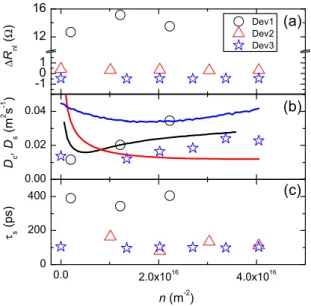
μsthe spin accumulation,Dsthe spin-diffusion constant, and τsthe spin-relaxation time. From the fitting of the Hanle spin signalsRnlmeasured at different carrier densities, we obtain the value ofτs to be lower than 280 ps for Dev1, 80 ps for Dev2, and 100 ps for Dev3.
To study the influence of the LR contacts on spin trans- port [24,35–37], we calculate the values of (Rc/Rs, L/λs) parameters. HereRs=Rsqλs/W is the spin resistance of the graphene with λs=√
Dsτs, the spin-relaxation length, and the ratioRc/Rsquantifies the back-flow of injected spins into the contacts [24]. For the devices Dev1, Dev2, and Dev3 at different carrier densities, we find the values of (Rc/Rs,L/λs) in the range of (0.81–12.97, 0.61–1.14), (0.12–3.11, 0.15–
2.65), and (13.64–77.81, 0.84–1.19), respectively. According to the analysis by Maassen et al. [24] on contact-induced spin relaxation in Hanle spin-precession measurements, the low-Rc/Rs values for Dev1 and Dev2 indicate that the spin relaxation in graphene is influenced by spin absorption at the LR contacts and resulted in underestimated values of the spin-transport parameters obtained via Hanle data fitting.
Therefore, we estimate the true values ofDsandτs for Dev1 and Dev2 by taking the effect of the low-Rc/Rscontacts into account [24]. For Dev3, high values of Rc/Rs indicate that the spin absorption by contacts is negligible, and we can safely assume that the fitted values of Ds and τs represent the true values. For all devices, the corrected values ofDs andτsare plotted in Figs.3(b)and3(c)as a function of the electron carrier density. For Dev1 and Dev3, we observe a good correspondence between the values ofDcandDswithin a factor of 2, confirming the reliability of our analysis [10,38].
After the correction, the value ofτsincreased to 400 ps for Dev1 and to 160 ps for Dev2. Even after the correction, such a low value ofτsfor these devices indicates that the spin relaxation within the graphene channel is dominant.
IV. DISCUSSION
To prepare our devices using CVD-hBN barriers, we used a similar method to that of Fu et al. [19] and Kamalakar et al.[18,21], except we used additionally a thick-exfoliated-
0.00 0.02 0.04
0.0 2.0x10¹⁶ 4.0x10¹⁶
0 200 400 -101 12 16
(c) (b)
Dc,Ds(m2 s-1 )
(a)
τs(ps)
n(m-2)
Dev1 Dev2 Dev3 ΔRnl(Ω)
FIG. 3. Data extracted from the Hanle spin-precession measure- ments for devices Dev1, Dev2, and Dev3 at different electron carrier densities. (a) Nonlocal Hanle spin-precession signalRnl=(RnlP− RnlAP)/2 atBz=0. Note thatRnlfor Dev3 (for set1 contacts) remains negative for all densities. (b) Carrier diffusion constants determined from the chargeDc, and the spinDs transport measurements, lines, and symbols, respectively.Dsfor Dev2 is not given due to unreliable values obtained from the Hanle fitting. We assumeDs=Dc[33] for Dev2 and useDcvalues to fit the Hanle dataRnl(Bz), and we obtain τs.Dcfor Dev3 is calculated from the effective density of states of three-layer graphene [34]. (c) Spin relaxation timesτs.
hBN as a substrate. However, despite having the bottom-hBN substrate, we do not observe an enhancement in the mobility of graphene [4].
From Fig.3(c), it is clear that even after including the correc- tion from the spin absorption due to the low-Rc/Rs contacts [24], the value of τs is still lower than 400 ps for all three devices. We do not observe an increasedτsin our devices with two-layer-CVD-hBN encapsulating tunnel barriers, compared to the monolayer-CVD-hBN [18–20] encapsulating barriers.
In contrast, in the case of an exfoliated-hBN encapsulating tunnel barrier, increasing the number of layers from monolayer to bilayer resulted in an increase of τs due to large RcA contacts and enhanced screening of polymer contamination by bilayer-hBN [14–17].
The lower values of spin-relaxation times and mobilities for our hBN-based graphene devices with top CVD-hBN tunnel barrier encapsulation can be attributed to several factors, such as the quality of graphene due to the wet transfer process, the nonuniform CVD-hBN barrier, their improper interface, and the proximity of the lithography residues. The growth of CVD- hBN can suffer from the inhomogeneous surface coverage, and the copper etching steps could also damage the CVD- hBN and leave some underetched residues, leading to uneven interfacial growth of ferromagnetic cobalt on top [15], which may cause spin dephasing in graphene via randomly oriented magnetic fringe fields near the contacts [39]. Moreover, during the wet transfer of CVD-hBN, some unwanted contamination may get trapped at the interface with graphene, and graphene itself comes in direct contact with DI water. Even though we dry
0 4 8 12
0 2 4 6 8
0.0 0.4 0.8 0
1 Dev1
Dev2 Dev3
ΔEY= 0.5 0.6 meV ΔDP= 74 31μeV ΔDP= 215 142μeV
ε2 Fτ p/τ s(10-5 eV2 )
ε2Fτ2p(10-28eV2ps2)
ΔEY= 2.1 1.9 meV ΔDP= 86 26μeV
FIG. 4. The linear fits (solid lines) of the data using Eq. (1) give the spin-orbit coupling strengths of the EY and DP spin-relaxation mechanisms,EYandDP, respectively, for three devices. The inset shows the data and fits close to zero. A reliable value ofEYfor Dev2 is not obtained due to the nonmonotonic relation betweenτsandn[4]
[see Fig.3(c)].
the stack right after the transfer of CVD-hBN on a hot plate, we do not know how many impurities are removed. Furthermore, we use a two-layer (not the as-grown bilayer) CVD-hBN tunnel barrier, which may come with additional Cu residues, water molecules, or any hydrocarbon molecules trapped in between the two hBN layers from the preparation steps. During the transfer of one CVD-hBN layer on top of another, even folding or shrinking of the individual layers can occur.
To investigate the possible spin-relaxation phenomenon causing the low spin relaxation times for graphene in our devices, we analyze the data in Fig. 3 by following Zomer et al.[4]. We consider Elliott-Yafet (EY) and D’Yakonov- Perel’ (DP) mechanisms contributing to the spin relaxation in graphene, and we analyze the relation between τs and momentum relaxation time,τp, using the equation [4]
ε2Fτp
τs =2EY+ 42DP
¯ h2
ε2Fτp2, (1)
whereεFis the Fermi energy of graphene, andEYandDPare the spin-orbit coupling strengths of EY and DP mechanisms, respectively.
The fits to the data for three devices, shown in Fig.4, using the above equation giveEYandDP. We calculate the spin- relaxation rates due to EY and DP mechanisms fromτs,EY−1 =
2EY
εF2τp andτs,DP−1 = 4h¯2DP2τp. The values of (τs,EY−1 ,τs,DP−1 ) for Dev1, Dev2, and Dev3 are found to be in the range of (0.2–2.7, 2.0–
2.5) ns−1, (–, 10.3–13.8) ns−1, and (0.6–1.8, 8.4–9.4) ns−1. Due to the nonlinear nature of the plotted data for Dev2, it cannot be accurately fitted with Eq. (1). The relaxation rates for both EY and DP mechanisms are in the similar order of 109s−1, and a clear dominance of either of the mechanisms cannot be distinguished.
From the regular spin valve and Hanle signals for Dev1 [Figs. 2(b) and 2(e)], it is evident that the differential spin polarizations of the LR and the HR contacts have the same sign. On the contrary, from the inverted spin valve and Hanle signals for Dev3 [Figs.2(d)and2(g)for set1], at zero dc bias (Vin=0 V), we deduce that the spin polarization of the HR
contact has an opposite sign with respect to that of the LR contact.
Note that the absolute sign of the spin polarization cannot be determined from the nonlocal spin-transport measurements.
For each device, we assume the polarization of the LR contact to be positive. Therefore, for the two-layer-CVD-hBN tunnel barrier contacts, we find both positive and negative spin polar- izations for the HR contacts (in the range 4.7–10.8 k μm2) with respect to the LR contacts (in the range 1.0–2.4 k μm2), i.e., there is no consistent correlation between theRcAvalues of the HR contacts and their polarization signs (positive or negative). This behavior is different from the results reported by Kamalakaret al.[21], wherein a layer of CVD-hBN tunnel barrier with variable thickness (one to three layers) is used, and the sign of the spin polarization is reported to be positive only for the contacts with RcA25 k μm2 and negative for RcA170 k μm2. The authors of Ref. [21] used a layer of CVD-hBN with a spatial distribution of thickness varied between one and three layers. Note, however, that this multilayer-CVD-hBN has not been layer-by-layer-stacked but as-grown with inhomogeneous thickness, and the observed behavior was attributed to the spin-filtering at the cobalt/hBN interface. Since we do not have a perfect Bernal-stacked bilayer CVD-hBN tunnel barrier, we cannot comment on the possible spin-filtering mechanism for the negative polarization of the HR contacts observed here.
In fact, a recent study with bilayer-exfoliated-hBN barriers by Gurramet al.[16] reported that at zero dc bias, different contacts (with RcAin the range 4.6–77.1 k μm2) showed different signs (positive or negative) of differential spin polar- izations, which is also observed here with the two-layer-CVD- hBN barriers. However, in contrast to the layer-layer-stacked two-layer-CVD-hBN, mechanically exfoliated bilayer-hBN is expected to have a crystallographic orientation. Therefore, it makes it more difficult to comment on a possible mechanism causing negative polarization.
Now we study the bias dependence of the differential spin signalsRnland differential spin-injection polarization pin of the two-layer-CVD-hBN contacts. A recent report by Gurram et al. [16] on the effect of bias applied across the ferromagnetic contacts with a bilayer-exfoliated-hBN barrier revealed a dramatic behavior ofRnlandpin, where the sign of the differential polarization is reversed at a very small bias, and its magnitude is increased with bias even up to 100%. In light of these results, it is interesting to study the bias dependence of thepinof the two-layer-CVD-hBN barrier contacts.
In the case of application of a bias across a ferromagnetic tunneling contact with transparent regions (i.e., a tunnel barrier with pinholes), one would observe an increase (decrease) in the magnitude of the spin signal with positive bias for holes (electrons) [11] due to a strong local carrier drift in graphene underneath the metallic electrode. Moreover, the carrier density in graphene underneath such contacts can- not be modified via the backgate voltage as it is partially screened by the proximity of the metal electrode. For fer- romagnetic tunneling contacts (i.e., a tunnel barrier without any pinholes), since the voltage drop occurs across the tunnel barrier, one can study the bias-induced polarization of the contacts [16,21].
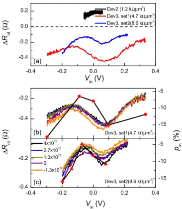
FIG. 5. (a) Nonlocal differential spin signalRnlas a function of the injection biasVinfor Dev2 with LR-LR injector-detector contacts pair, and for Dev3 with two different sets of HR-LR injector-detector contacts pairs. Inversion of the spin signal for Dev3 is due to the inverse polarization of the HR injector contact with respect to the LR detector [see Figs.2(d)and2(g)for set1]. The dashed line represents Rnl=0.RcA values of the respective injector contacts, at zero bias, are given in the legend. The left axis of (b) and (c) shows bias-dependentRnlfor set1 and set2 contacts of Dev3, respectively, at different carrier densities ranging from electrons (n >0) to holes (n <0). The legend in (c) shows the carrier density in cm−2. The right axis of (b) and (c) shows differential spin-injection polarizationpin
at an electron density of 3.4×1012cm−2for set1 and 4×1012cm−2 for set2, respectively.
To bias the injector contact, we sweep dc current bias (Iin) along with a fixed amplitude of ac current i=1 μA.
We use the standard lock-in detection technique to measure the voltage (v) across the nonlocal detector contacts, and we obtain the nonlocal differential resistanceRnl(Iin)= vi at each value of the applied injection current biasIin. Figure5shows the nonlocal differential spin signalsRnl=(RPnl−RnlAP)/2, measured at zero magnetic field, as a function of the bias applied across the injector contacts in Dev2 and Dev3.
For Dev2 with LR contacts, application of the current bias up to±50μA (equivalent voltage bias,Vin≈ ±0.07 V) across the injector resulted in a small change in Rnl of around 0.06[Fig.5(a)]. The signalRnlis measured when the entire graphene channel isp-type at the carrier density n= −5× 1012cm−2. Within the bias range of±0.07 V, the magnitude ofRnlincreases (decreases) with the positive (negative) bias.
Therefore, this behavior could be due to transparent regions of the LR injector resulting in a finite voltage drop in the graphene leading to a strong local carrier drift underneath the metallic Co electrode [11].
For Dev3, Fig.5(a)shows two sets (labeled set1 and set2) of data for two different injector-detector contacts pairs. Each set consists of a HR injector and a LR detector. Under zero bias condition, i.e.,Vin=0, both sets show an inverted spin valve and Hanle signalsRnl[shown in Figs.2(d)and2(g)for set1].
When a dc current bias is applied across the injector contact up to±40μA (equivalent voltage biasVin≈ ±0.3 V for set1, and≈±0.2 V for set2), the value ofRnlchanges in a peculiar way, which is independent of the gate voltage [Figs.5(b)and 5(c)for set1 and set2, respectively]. The sign ofRnlremains the same within the applied gate and bias range. Interestingly, the magnitude ofRnlincreases at large negative bias.
The bias-dependent spin signalsRnlfor Dev3 in Fig.5(a) are measured when the entire graphene channel is n-type.
Within the bias range±0.3 V for set1 and±0.2 V for set2, the magnitude ofRnl increased (decreased) for the higher negative (positive) bias. Moreover, we also measured the same behavior when the carrier density of the graphene between the electrodes was changed to the vicinity of the charge-neutrality point and to thep-type, using the backgate voltage [Figs.5(b) and5(c)]. These observations imply that the carrier density in graphene underneath the contact is screened by the metallic Co electrode due to possible transparent regions in the HR injectors of Dev3. Due to the HR nature of the injectors in Dev3, the voltage drop is mostly across the two-layer-CVD- hBN tunnel barrier. At a small bias range close to zero, we observe a peculiar behavior ofRnlthat does not comply with the contact-induced local carrier drift [11]. We attribute this behavior to bias-induced spin polarization of the two-layer- CVD-hBN tunnel barrier.
We also measured Hanle spin signals Rnl(Bz) at dif- ferent injection current biases for set1 and set2 contacts of Dev3. Using the values of λs obtained from the fitting of Rnl(Bz) data measured at different injection bias, we calculatepinof the (inner) injector contact using the following equation [10]:
Rnl=pinpd
Rsqλse−λsL 2W
, (2)
wherepdis the differential spin-detection polarization of the (inner) detector. We assume that pd is constant, as the bias is applied only across the injector contact, and is equal to the unbiased pin of the injector, i.e.,pd=pin(Vin=0). The resultingpinat different injection bias voltages for the injectors in set1 and set2 are shown on the righty axes of Figs. 5(b) and 5(c), respectively. The change in pin as a function of bias nearly follows the change inRnl, and the sign of pin remains negative. Moreover, the magnitude of bothRnland pin increases at higher negative bias, and the value of pin reaches up to−15% at−0.3 V for set1, and at−0.2 V for set2 contacts of Dev3.
Kamalakaret al.[21] showed a similar inversion behavior of spin signals for thicker (two to three layers) CVD-hBN barriers over a large range of bias,±2 V, where the magnitude of the spin signal decreases at large injection bias voltages|Vin|>
0.5 V. However, the authors of Ref. [21] do not report the data for smaller bias voltages|Vin|<0.5 V, the range within which we measure the differential spin signalRnl and differential spin polarizationpin(|Vin|<0.3 V). Note that we used the low-
frequency lock-in detection technique, which helps to measure the spin signals even at a very small dc bias [16], which is difficult with the pure dc measurements [21]. On the other hand, a recent report by Gurramet al.[16] with a bilayer-exfoliated- hBN tunnel barrier showed a dramatic change in Rnl and pin with the applied bias, and their sign inversion was near zero bias. We do not observe such inversion in the sign of the spin signals with bias for the two-layer-CVD-hBN barriers.
This points to the different nature of the bilayer-exfoliated- hBN and two-layer-CVD-hBN tunnel barriers with respect to spin injection.
V. CONCLUSIONS
In conclusion, we have investigated room-temperature spin transport in graphene, encapsulated by a layer-by-layer- stacked two-layer-CVD-hBN tunnel barrier and a few-layer- thick exfoliated-hBN substrate. Even though the graphene is supported by the bottom-hBN substrate, its mobility is quite low and thus resulted in small diffusion constants. The lower values of mobilities and spin-relaxation times compared to the already reported graphene on hBN devices are attributed to the conventional wet transfer technique used for transferring the CVD-hBN tunnel barrier, and possible copper residues trapped in between the two CVD-hBN monolayers and at the interface with graphene. We analyze the spin-transport data by considering Elliott-Yafet and D’Yakonov-Perel’ spin- relaxation mechanisms, and we find no clear dominance of either of the mechanisms.
For the cobalt/two-layer-CVD-hBN/graphene/hBN con- tacts, we find no correlation between the RcA values of high-resistive contacts and the sign of the spin polarization.
Furthermore, spin polarization of the high-resistance contacts remains reversed with respect to the low-resistance contacts, within ±0.3 V bias, and its magnitude increases at large negative bias. This behavior is different from what has been reported for the contacts with high-resistive thick-CVD-hBN barriers, bilayer-exfoliated-hBN barriers, and oxide barriers.
We emphasize that the two-layer barrier is different from the bilayer, where the former is just an assembly of two indi- vidual monolayers and the latter is as-grown. Despite having equivalent thicknesses, the two-layer-CVD-hBN barrier shows a completely different bias dependence of the spin injection compared to that of the bilayer-exfoliated-hBN barrier [16].
This implies that the quality and the relative alignment of two monolayers of hBN might play a significant role in determining the tunneling characteristics.
We observe a large magnitude of differential spin polariza- tion up to 15% at−0.2 V bias, and it could be enhanced further with application of higher bias for high-resistance contacts with two-layer-CVD-hBN barriers, which is promising for spintronics applications. However, in order to establish the role of CVD-based hBN in graphene spintronics, it is important to prepare a clean device without hampering the quality of graphene for long-distance spin transport. For this purpose, the recently proposed dry transfer technique for CVD-grown materials [40] could be adopted to greatly improve the quality of graphene spin-valve devices. Furthermore, we expect that a controlled growth of bilayer-CVD-hBN [26] tunnel barriers followed by dry transfer on top of recently obtained high-
quality CVD graphene [41] could help to expand the role of CVD-grown materials for spintronics in van der Waals heterostructures.
ACKNOWLEDGMENTS
We kindly acknowledge J. G. Holstein, H. M. de Roosz, H. Adema, and T. J. Schouten for technical assistance. The
research leading to these results has received funding from the European Union’s Horizon 2020 research and innovation programme under Grant Agreement No. 696656 Graphene Flagship, Swiss Nanoscience Institute, Swiss National Science Foundation, iSpinText FlagERA project, National Natural Science Foundation of China (Grant No. 51290272), and it was supported by the Zernike Institute for Advanced Materials and the Nederlandse Organisatie voor Wetenschappelijk (NWO).
[1] L. Britnell, R. V. Gorbachev, A. K. Geim, L. A. Ponomarenko, A. Mishchenko, M. T. Greenaway, T. M. Fromhold, K. S.
Novoselov, and L. Eaves,Nat. Commun.4,1794(2013).
[2] L. Wang, I. Meric, P. Y. Huang, Q. Gao, Y. Gao, H. Tran, T.
Taniguchi, K. Watanabe, L. M. Campos, D. A. Muller, J. Guo, P. Kim, J. Hone, K. L. Shepard, and C. R. Dean,Science342, 614(2013).
[3] J. Wang, F. Ma, W. Liang, and M. Sun,Mater. Today Phys.2,6 (2017).
[4] P. J. Zomer, M. H. D. Guimarães, N. Tombros, and B. J. van Wees,Phys. Rev. B86,161416(2012).
[5] M. H. D. Guimarães, P. J. Zomer, J. Ingla-Aynés, J. C. Brant, N. Tombros, and B. J. van Wees,Phys. Rev. Lett.113,086602 (2014).
[6] J. Ingla-Aynés, M. H. D. Guimarães, R. J. Meijerink, P. J. Zomer, and B. J. van Wees,Phys. Rev. B92,201410(2015).
[7] S. Roche, J. ˚Akerman, B. Beschoten, J.-C. Charlier, M. Chshiev, S. Prasad Dash, B. Dlubak, J. Fabian, A. Fert, M. Guimarães, F.
Guinea, I. Grigorieva, C. Schönenberger, P. Seneor, C. Stampfer, S. O. Valenzuela, X. Waintal, and B. J. van Wees,2D Mater.2, 030202(2015).
[8] J. Ingla-Aynés, R. J. Meijerink, and B. J. van Wees,Nano Lett.
16,4825(2016).
[9] W. Han, K. Pi, K. M. McCreary, Y. Li, J. J. I. Wong, A. G. Swartz, and R. K. Kawakami,Phys. Rev. Lett.105,167202(2010).
[10] N. Tombros, C. Józsa, M. Popinciuc, H. T. Jonkman, and B. J.
van Wees,Nature (London)448,571(2007).
[11] C. Józsa, M. Popinciuc, N. Tombros, H. T. Jonkman, and B. J.
van Wees,Phys. Rev. B79,081402(2009).
[12] L. Britnell, R. V. Gorbachev, R. Jalil, B. D. Belle, F. Schedin, M. I. Katsnelson, L. Eaves, S. V. Morozov, A. S. Mayorov, N.
M. R. Peres, A. H. Castro Neto, J. Leist, A. K. Geim, L. A.
Ponomarenko, and K. S. Novoselov,Nano Lett.12,1707(2012).
[13] T. Yamaguchi, Y. Inoue, S. Masubuchi, S. Morikawa, M. Onuki, K. Watanabe, T. Taniguchi, R. Moriya, and T. Machida,Appl.
Phys. Express6,073001(2013).
[14] M. Gurram, S. Omar, S. Zihlmann, P. Makk, C. Schönenberger, and B. J. van Wees,Phys. Rev. B93,115441(2016).
[15] S. Singh, J. Katoch, J. Xu, C. Tan, T. Zhu, W. Amamou, J. Hone, and R. Kawakami, Appl. Phys. Lett. 109, 122411 (2016).
[16] M. Gurram, S. Omar, and B. J. van Wees,Nat. Commun.8,248 (2017).
[17] M. Gurram, S. Omar, and B. J. van Wees,arXiv:1712.07828.
[18] M. V. Kamalakar, A. Dankert, J. Bergsten, T. Ive, and S. P. Dash, Sci. Rep.4,6146(2014).
[19] W. Fu, P. Makk, R. Maurand, M. Bräuninger, and C.
Schönenberger,J. Appl. Phys.116,074306(2014).
[20] M. V. Kamalakar, A. Dankert, J. Bergsten, T. Ive, and S. P. Dash, Appl. Phys. Lett.105,212405(2014).
[21] M. V. Kamalakar, A. Dankert, P. J. Kelly, and S. P. Dash,Sci.
Rep.6,21168(2016).
[22] A. Dankert, M. V. Kamalakar, A. Wajid, R. S. Patel, and S. P.
Dash,Nano Res.8,1357(2015).
[23] M. Piquemal-Banci, R. Galceran, S. Caneva, M.-B. Martin, R.
S. Weatherup, P. R. Kidambi, K. Bouzehouane, S. Xavier, A.
Anane, F. Petroff, A. Fert, J. Robertson, S. Hofmann, B. Dlubak, and P. Seneor,Appl. Phys. Lett.108,102404(2016).
[24] T. Maassen, I. J. Vera-Marun, M. H. D. Guimarães, and B. J. van Wees,Phys. Rev. B86,235408(2012).
[25] Q. Wu, L. Shen, Z. Bai, M. Zeng, M. Yang, Z. Huang, and Y. P.
Feng,Phys. Rev. Appl.2,044008(2014).
[26] Y. Gao, W. Ren, T. Ma, Z. Liu, Y. Zhang, W.-B. Liu, L.-P. Ma, X. Ma, and H.-M. Cheng,ACS Nano7,5199(2013).
[27] X. Song, J. Gao, Y. Nie, T. Gao, J. Sun, D. Ma, Q. Li, Y. Chen, C. Jin, A. Bachmatiuket al.,Nano Res.8,3164(2015).
[28] P. J. Zomer, M. H. D. Guimarães, J. C. Brant, N. Tombros, and B. J. van Wees,Appl. Phys. Lett.105,013101(2014).
[29] Y. Lee, S. Bae, H. Jang, S. Jang, S.-E. Zhu, S. H. Sim, Y. I. Song, B. H. Hong, and J.-H. Ahn,Nano Lett.10,490(2010).
[30] K. S. Novoselov, A. K. Geim, S. V. Morozov, D. Jiang, Y. Zhang, S. V. Dubonos, I. V. Grigorieva, and A. A. Firsov,Science306, 666(2004).
[31] P. Zomer, S. Dash, N. Tombros, and B. Van Wees,Appl. Phys.
Lett.99,232104(2011).
[32] K. Nagashio, T. Nishimura, K. Kita, and A. Toriumi,Jpn. J. Appl.
Phys.49,051304(2010).
[33] C. P. Weber, N. Gedik, J. E. Moore, J. Orenstein, J.
Stephens, and D. D. Awschalom,Nature (London)437,1330 (2005).
[34] T. Maassen, F. K. Dejene, M. H. D. Guimarães, C. Józsa, and B.
J. van Wees,Phys. Rev. B83,115410(2011).
[35] E. Sosenko, H. Wei, and V. Aji, Phys. Rev. B 89, 245436 (2014).
[36] H. Idzuchi, A. Fert, and Y. Otani,Phys. Rev. B 91, 241407 (2015).
[37] G. Stecklein, P. A. Crowell, J. Li, Y. Anugrah, Q. Su, and S. J.
Koester,Phys. Rev. Appl.6,054015(2016).
[38] M. H. D. Guimarães, A. Veligura, P. J. Zomer, T. Maassen, I.
J. Vera-Marun, N. Tombros, and B. J. van Wees,Nano Lett.12, 3512(2012).
[39] S. P. Dash, S. Sharma, J. C. Le Breton, J. Peiro, H. Jaffrès, J.-M.
George, A. Lemaitre, and R. Jansen,Phys. Rev. B84,054410 (2011).
[40] M. Drögeler, L. Banszerus, F. Volmer, T. Taniguchi, K.
Watanabe, B. Beschoten, and C. Stampfer, Appl. Phys. Lett.
111,152402(2017).
[41] L. Banszerus, M. Schmitz, S. Engels, J. Dauber, M. Oellers, F. Haupt, K. Watanabe, T. Taniguchi, B. Beschoten, and C.
Stampfer,Sci. Adv.1,e1500222(2015).