ARTICLE
OPENRobust quantum point contact operation of narrow graphene constrictions patterned by AFM cleavage lithography
Péter Kun 1✉, Bálint Fülöp 2,3, Gergely Dobrik1, Péter Nemes-Incze 1, István Endre Lukács1, Szabolcs Csonka2,3, Chanyong Hwang 4and Levente Tapasztó 1✉
Detecting conductance quantization in graphene nanostructures turned out more challenging than expected. The observation of well-defined conductance plateaus through graphene nanoconstrictions so far has only been accessible in the highest quality suspended or h-BN encapsulated devices. However, reaching low conductance quanta in zero magneticfield, is a delicate task even with such ultra-high mobility devices. Here, we demonstrate a simple AFM-based nanopatterning technique for defining graphene constrictions with high precision (down to 10 nm width) and reduced edge-roughness (+/−1 nm). The patterning process is based on the in-plane mechanical cleavage of graphene by the AFM tip, along its high symmetry crystallographic directions. As-defined, narrow graphene constrictions with improved edge quality enable an unprecedentedly robust QPC operation, allowing the observation of conductance quantization even on standard SiO2/Si substrates, down to low conductance quanta. Conductance plateaus, were observed atn× e2/h, evenly spaced by 2 × e2/h(corresponding ton=3, 5, 7, 9, 11) in the absence of an external magneticfield, while spaced by e2/h(n=1, 2, 3, 4, 5, 6) in 8 T magneticfield.
npj 2D Materials and Applications (2020) 4:43 ; https://doi.org/10.1038/s41699-020-00177-x
INTRODUCTION
Due to its mechanical, optical, and electronic properties, graphene has been at the forefront of low dimensional materials research for fifteen years, starting with the early discovery of the half-integer quantum Hall effect and non-zero Berry phase1,2. Due to its outstanding electronic quality, manifesting itself in particularly high charge carrier mobility3 and long coherence lengths4, enormous efforts have been invested into realizing graphene- based quantum devices5–7. However, one of the most fundamental quantum size effects, the precise detection of charge quantization in graphene nanoconstrictions turned out to be particularly challenging, hindering the implementation of graphene-based quantum point contacts.
Before the discovery of 2D crystals, the research on quantum transport phenomena focused on two-dimensional electron systems in semiconductor nanostructures8. Among others, quan- tum point contacts (QPC)—a narrow constriction between two extended electrically conducting areas—have been realized, conventionally through charge carrier depletion with the help of split-gate electrodes9,10. Similarly, in bilayer graphene, a transverse electricfield can open a band gap11, which allows for depletion of the gated area, but the full pinch-off state is hard to achieve due to leakage currents. Recently, by improved device fabrication, this obstacle has been removed, allowing the observation of con- ductance quantization, unexpected mode crossings12,13, as well as the interplay between spin-orbit coupling and electron-electron interaction at zero magneticfield14. However, the presence of AB- BA stacking domain walls cannot be fully avoided in bilayer samples15. Acting as current leakage pathways, they limit the reliability of the bilayer QPC device fabrication process.
By contrast, in the case of monolayer graphene, employing a similar split-gate geometry cannot induce a complete electrical depletion, instead it leads to the formation of p-n junctions,
short-circuiting the constriction16. Nonetheless, the physical removal of material (etching, cutting) provides a viable solution to overcome this problem, and to realize confinement. In this case, the main factors defining the electronic transport characteristics are the charge carrier mobility in graphene and the structural quality of the constriction edges. A major bottle- neck is the extended charge localization area, implying that the detrimental effects of edge disorder are felt even relatively far from the constriction17. Even so, signatures of quantized conductance have been reported in graphene constrictions.
Tombros et al. applied a high current annealing method on suspended graphene18. Quantized edge modes have also been observed in tapered brides formed during the exfoliation of graphene by a metallic tip19. However, similar techniques offer a limited control on the width and geometry of the constriction. E- beam lithography combined with etching is the most wide- spread nanofabrication technique for graphene quantum QPCs20. Although, e-beam lithography is capable of defining constrictions down to a few tens of nanometers width, the size of the investigated constrictions is typically in the hundred nanometers range. This is required to mitigate the effect of edge disorder21 that precludes obtaining well-defined QPC characteristics in narrower constrictions. However, to reach lower conductance quanta, in such wide constrictions, the Fermi wavelength of graphene has to be of comparable scale to the constriction width. This imposes highly demanding requirements on the graphene quality for enabling QPC operation. Such requirements can only be met by suspending graphene or encapsulating it between hexagonal boron nitride layers. Only in the best ultra-high mobility devices can the signatures of size quantization be observed, in the form of more or less evenly spaced modulations (kinks) superimposed on the linear con- ductance22–25. However, in the absence of magneticfield, these
1Centre for Energy Research, Institute of Technical Physics and Materials Science, 1121 Budapest, Hungary.2Department of Physics, Budapest University of Technology and Economics, 1111 Budapest, Hungary.3MTA-BME“Momentum”Nanoelectronics Research Group, H-1111 Budapest, Hungary.4Korea Research Institute for Standards and Science, Daejeon 305340, South Korea.✉email: kun@mfa.kfki.hu; tapaszto@mfa.kfki.hu
1234567890():,;
plateaus only become well-defined further away from the Dirac point, corresponding to high conductance quanta (typically,σ>
10 e2/h). Reducing the constriction width is important as it can ensure a more robust QPC operation, allowing the observation of plateaus at lower conductance quanta, and enabling QPC characteristics to persist up to higher temperatures, by increas- ing the energy separation between transversal modes. However, reducing the constriction width cannot be efficient without improving the edge quality. These are two of the next important steps towards improving the feasibility and reliability of graphene QPCs.
Besides e-beam lithography, scanning probe microscopy-based techniques can also be employed for patterning graphene.
For instance, AFM-based local anodic oxidation lithography has been applied on graphene to form nanoribbons, quantum dots or nanorings, by etching, down to 30-nm-wide, insulating trenches26–28. The precise direct mechanical cutting of graphene by AFM turned out quite difficult, as graphene tends to tear and fold along various directions during the scratching29. An under- lying thin layer of polymethyl methacrylate (PMMA)30 has been employed, to provide stronger adhesion to the substrate, and improve the cutting precision. On conducting substrates scanning tunneling microscope lithography can be employed, for defining graphene nanoribbons with nanometer precision31,32. However, the conductive substrates required by STM do not allow the direct integration of the patterned graphene structures into electronic devices.
Here, we have developed an improved AFM lithographic method enabling a much more precise direct mechanical patterning (in-plane cleavage) of graphene sheets. This technique enabled us to define graphene nanoconstrictions down to 10 nm
width, with edges of improved structural quality (lower rough- ness), by cleaving the graphene sheet along its high symmetry crystallographic directions (armchair, zigzag). The as-defined graphene nanoconstrictions allow the observation of conductance quantization down to a few conductance quanta, even on standard SiO2/Si substrates, at temperatures up to 40 K.
RESULTS AND DISCUSSION
AFM cleavage lithography of graphene
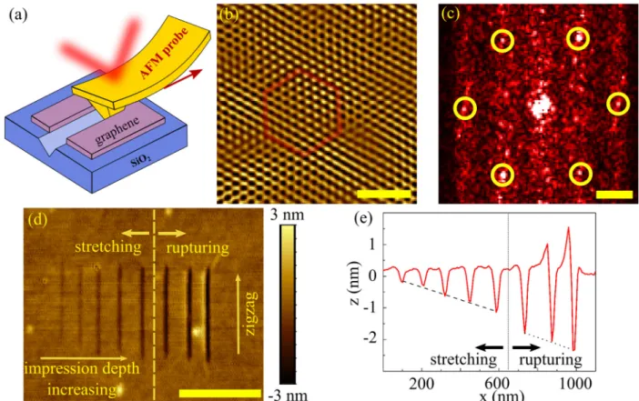
Graphene samples have been prepared by micromechanical exfoliation on the most commonly used silicon substrate with 285 nm SiO2 capping layer (see Supplementary Fig. 1). For defining high-quality graphene constrictions with high precision, we have developed an improved AFM-based lithographic technique (Fig. 1a). To enable this, we have exploited the capability of AFM to determine the crystallographic orientations of the graphene lattice before patterning33. By imaging the surface in contact mode, the atomic potentials modulate the friction forces between tip and sample, revealing the high symmetry lattice directions of the graphene sheet (Fig. 1b, c).
This enables us to choose the precise crystallographic orientation of the cutting direction, which—as it turns out—is of key importance for defining high quality edges. For cutting the graphene sheet, the AFM tip is lowered and pushed into the sample surface to a predetermined deflection (corresponding to 100–200 nm apparent lowering of the tip, depending on the force constant), with the feedback-loop switched off. Then, the tip is moved along the line of the desired cutting direction (Fig. 1d).
Considering the outstanding tensile strength of graphene, for low indentation depths graphene is only stretched, adhering to the
Fig. 1 AFM-based in-plane mechanical cleavage of graphene. aSchematic of the AFM cleavage lithography process.bLattice resolution on graphene acquired in contact mode, (FFT filtered for clarity), revealing the main crystallographic directions. Scale bar: 2 nm. c Fourier transform of the original lattice resolution image. Scale bar: 2 nm−1.dLinear AFM indentations in graphene along zigzag direction with gradually increasing depth. Scale bar: 500 nm.eDepth profiles of the patterned lines from paneld, revealing the border between stretching and cutting of the graphene sheet.
2
1234567890():,;
surface of the plastically deformed underlying silica substrate34. After reaching the indentation depth of approximately 1.5 nm, the chances of graphene rupture increase dramatically, in accordance with our previousfindings35.
On Fig.1d, linear patterns running along a zigzag direction can be seen, prepared with gradually increased indentation depth. As a result of the smooth edges of the indentation line, it is hard to differentiate, when the graphene layer is cut instead of just being pushed/stretched into the groove of the substrate. However, by analyzing the line profiles (Fig. 1e) the two regions can be distinguished. Further confirmation of the successful cutting of graphene comes from Raman spectroscopy mapping, where the D peak intensity is highly sensitive to the presence of edges (see Supplementary Fig. 3).
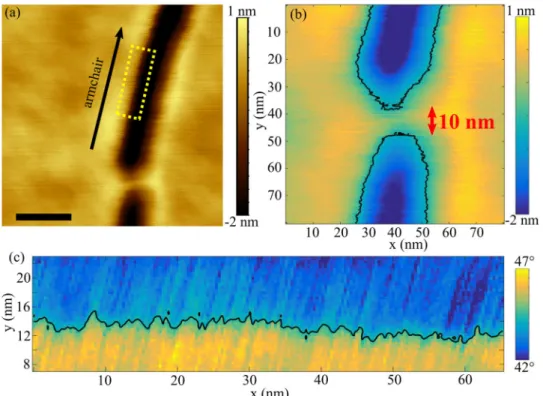
Graphene constrictions can be formed by cutting two lines with one of their ends in close proximity, and the other ends reaching the edges of theflake. This, results in a narrow bridge between two large and intact graphene areas. To demonstrate the precision of our nanolithography technique in Fig.2we show the topography of an approximately 10 nm wide constriction with the cutting lines running along an armchair direction. Note that while the two cutting lines have the same (armchair) orientation relative to the graphene lattice, they are not perfectly aligned. This slight misalignment helps avoiding strong back- scattering, as discussed later. The smoothness of the edges is due to the fact, that graphene can be cut (cleaved) more easily along its high symmetry (armchair/zigzag) lattice directions36,37 (see also Supplementary Fig. 4). This is similar to cleaving bulk crystals along their high symmetry planes. Exploiting the useful ability of AFM to image and cut graphene along these easy cleaving directions, enables us to highly improve the precision of the nanofabrication process and reduce the roughness of edges. While the fabrication of graphene constrictions with
~10 nm width is still challenging, constrictions of a few tens of nanometers can be reliably defined by our AFM cleavage
lithography technique. To quantify the characteristic edge roughness, the phase image obtained in tapping mode proved to be the most suitable, as it reveals the boundaries more clearly than topographic images. The graphene edge—indicated by the black line in Fig.2c—is determined based on the deviation from the average value of the phase on the graphene sheet (44.4°). By analyzing the edge line, about +/−1 nm deviations can be measured from the averageyposition, indicating a ~2 nm edge roughness. This roughness is similar to that defined by cryo- etching of encapsulated graphene24, but achieved using a far simpler technique. The roughness of the short horizontal edge segment in Fig. 2, defining the nanoconstriction, can also be estimated, yielding a similar edge roughness of about+/−1 nm.
A more precise determination of the edge roughness is not feasible, since the scale of the observed roughness is on the verge of measurability by AFM, considering the practically achievable smallest tip radius of about 2 nm (see also Supplementary Fig. 5). Most importantly, our AFM based nanofabrication technique has the advantage of avoiding energetic beams and aggressive chemical etching that can induce additional disorder extending tens of nanometers inwards from the nominal edges20. Moreover, the quality of the edges is further preserved, since after the mechanical cleavage, constriction edges never come into contact with resist material or wet chemistry.
Residues generated by material removal during the AFM cleavage lithography, stick to the AFM tip. At the end position of the cutting, the tip often deposit debris (see Supplementary Fig.
2). To make sure that the leftover debris does not short circuit the constriction additional devices have been prepared, cutting across the whole graphene flake by AFM cleavage. The two-point resistance of such devices was in MΩrange, which is about two orders of magnitude higher than corresponding to conductance quanta, measured across constrictions, proving that the con- ductance of the cut section can be safely neglected.
Fig. 2 High resolution AFM cleavage lithography of graphene quantum point contacts. aTopographic tapping-mode AFM image of a 10 nm wide graphene constriction. Scale bar: 500 nm.bLocating the graphene edges.cEstimating the edge roughness from the phase image of the dashed rectangular area of Fig.2a: The black line marks the border of the step-like deviation from the average phase value on graphene.
3
Quantized conductance of graphene constrictions
Ti/Au (5/70 nm) electrodes have been defined on the graphene flakes by standard electron beam lithography technique prior to the AFM patterning step, to avoid the contamination of the constriction edges. To achieve lattice resolution AFM images, the resist residue has been eliminated by annealing in argon/
hydrogen atmosphere at 400 °C38. In addition, an AFM sweeping-based cleaning technique was also applied (see Supplementary Fig. 6.)39,40. Transport measurements in two- probe configuration have been performed at 1.5 K, using the heavily doped Si substrate as back-gate electrode. (Charge carrier mobility estimation can be found in Supplementary Fig. 8.) Plotting the conductance as a function of the applied gate voltage (Fig. 3a) for a ~75 nm wide constriction patterned by AFM cleavage lithography, reveals well-defined plateaus around G values of 3, 5, 7, 9, and 11e2/h, evidencing the conductance quantization, on top of the square root gate-dependence (see also Supplementary Fig. 7).
From the square root fitting of the G (Vg) characteristics, the width of the constriction can also be estimated. Using degeneracy factor of 2, and lever arm of α≈7.2 × 1010cm−2V−2, a channel length of W≈60 nm is obtained, which is in reasonably good agreement with the topographic AFM measurement (W≈75 nm) of the constriction. Similarly good agreement have been found for the other investigated constrictions (see Supplementary Fig. 7), supporting the interpretation of our results. For narrow constric- tions, contact resistances can be safely neglected (see also Supplementary Fig. 7). This is also confirmed by the fact that the conductance plateaus align reasonably well with n× e2/h values even without contact resistance corrections (Fig. 3). For graphene nanoribbons, conductance steps of 4 e2/h height are predicted41, where the factor of 4 comes from the spin and valley degeneracy of the charge carriers. However, as also reported earlier, graphene constrictions often display 2 e2/h conductance steps instead18,22–24, attributed to the lifting of the valley degeneracy. This is also predicted by the theoretical calculations of Guimarães et al. in which plateau-like features with a spacing of 2 e2/h can be observed in graphene nanoconstrictions that are less or equal in length than width (L≤W)42. Additional constric- tions fabricated by us by AFM lithography, display similar 2 e2/h steps, as can be seen in the Supplementary Fig. 9. We have also performed transport measurements with an externally applied (8T) magnetic field. The results shown in Fig. 3b. reveal conductance steps with roughly e2/h step heights. This can be attributed to the lifting of the spin degeneracy in addition to the lifted valley degeneracy. The phenomenon is similar to that
observed on QPC devices approaching the quantum Hall regime43. On the inset of Fig. 3. the layout of the devices, as well as the 3D topographic AFM images of the corresponding nanoconstrictions are shown. We note that constriction edges appear less regular than in Fig.2mainly due to less than optimal imaging conditions in order to preserve the structural integrity of the nanoconstrictions. The differences in the Vgvalues (xaxis of Fig.3) for different devices originate from the differences of the Dirac point position. A substantial p doping of the samples originates from the charged impurities in the SiO2substrate, as well as the annealing step employed for cleaning the samples from resist residues. Due to the relatively highpdoping levels of graphene in our devices, we were not able to measure the electron branch of the characteristics. However, the significant p doping, together with the slight misalignment of constriction ends, helps us approaching the adiabatic limit, and avoiding strong back-scattering, due to sharp changes of the constriction widths on the scale of the Fermi wavelength. We also note that we could not obtain reliable conductance characteristics for the narrowest (~10 nm wide) constrictions fabricated here, as they were broken very fast during the measurements. Nevertheless, constrictions as narrow as ~30 nm could be measured (Fig. 3b) displaying quantized conductance plateaus. Most constrictions also display oscillations superposed on the step-like conductance characteristics. This is commonly observed in QPC devices, and is often attributed to transmission resonances from reflections at the two ends of the constrictions, as well as quantum interference form impurity scattering near the constrictions8.
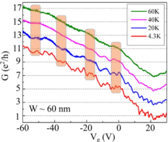
We have also investigated the temperature dependence of the QPC characteristics (Fig.4). In accordance with expectations, by increasing the temperature, the conductance plateaus are gradually smeared out, while also acquiring a finite slope, until they are no longer resolved. In our case, conductance plateaus could be clearly observed up to 20 K, and signatures of conductance quantization could be detected even at 40 K. This is in accordance with the estimated energy separation of transversal modes (~5 meV for 60 nm width), expected to persist up to ~3kBT (~5 meV at 20 K) thermal energy. Moreover, the energy separation of the transverse mode in the narrowest constriction fabricated by AFM lithography (order of 100 meV) is large enough for the QPC operation to persist even up to room temperature holding the promise of opening an entirely new regime for quantum point contact devices.
We have developed a high precision nanolithography techni- que for the fabrication of robust graphene quantum point contact devices. We showed that defining graphene constrictions through Fig. 3 Conductance measurements (1.5 K) of graphene QPCs patterned by AFM cleavage lithography with cuts running along zigzag directions.(Upper insets: optical images of the devices. Lower insets: 3D topographic AFM image of the nanoconstrictions, scale bars are 100 nm.)aTwo-probe conductance curve in zero magneticfield, for a ~75 nm wide constriction revealing conductance plateaus at integern× e2/hvalues separated by 2e2/h steps.b Two-probe conductance curve measured through a ~30 nm wide graphene constriction in 8 T magneticfield displaying quantization steps withe2/hspacing.
4
cleaving graphene sheets by AFM along their high symmetry directions, enables us to fabricate graphene nanoconstrictions down to 10 nm width and with reduced edge roughness of +/−1 nm. Narrow graphene constrictions with high quality edges display robust QPC behavior manifesting in well-defined zero-field conductance quantization plateaus down to a few conductance quanta, even on SiO2/Si substrates, and temperatures up to 40 K.
In zero magneticfield, evenly spaced conductance plateaus could be detected, roughly spaced by 2 e2/hattributed to the lifting of the valley degeneracy, while the application of magnetic field resulted in plateaus spaced by e2/h, indicating the lifting of both valley and spin degeneracy. Our AFM based nanopatterning technique enables the fabrication of robust graphene QPCs, lifting the highly demanding requirements for the device quality, prohibitive for most applications. Furthermore, such devices could also be employed as cheap resistance standards, providing precise resistance plateaus without requiring externally applied magnetic fields or very low temperatures for their reliable operation.
METHODS
Sample preparation
Graphene sheets have been prepared by mechanical exfoliation of natural graphite crystals, with the standard scotch tape method on Si/SiO2substrate.
Standard electron beam lithography (EBL) technique, followed by metal evaporation, has been utilized for device fabrication. To contact the graphene layer, Ti/Au (5/70 nm) has been evaporated at 10−8mbar. To improve the quality of the devices, a 1-h long annealing step has been performed in Ar:H2
atmosphere at 400 °C. Additional to this, cleaning of graphene by AFM sweeping has been carried out (see Supplementary Fig. 6).
Atomic force microscopy cleavage and characterization
For AFM imaging and patterning, a Bruker Multimode 8 AFM has been used, equipped with a closed loop scanner. For patterning, diamond-like carbon coated silicon AFM probes (Tap300DLC, Budget Sensors) have been used, with a nominal force constant of 40 N/m and a tip radius of 15 nm. The AFM cutting has been controlled by the NanoMan lithography software of Bruker.
For imaging the edges, AFM tips of 2 nm nominal tip radius (SSS-NCH type, NanoWorld) have been employed. The contact-mode AFM measurements have been carried out with contact tip (DNP-S10) characterized by nominal force constant of 0.06 N/m, and a tip radius of 10 nm.
Raman spectroscopy
For Raman mapping, a confocal Raman microscope system (Witec Alpha 300 RSA) has been used with Nd:YAG laser (532 nm, 2 mW).
Electrical characterization
Transport measurements have been performed at 1.5 K in two-probe configuration using standard lock-in techniques at f=177 Hz and AC excitation voltageVAC=10 µV with a Stanford SR-830 lock-in amplifier and external low-noiseI/Vconverter.
DATA AVAILABILITY
The authors confirm that the data supporting thefindings of this study are available within the article. Related additional data are available on reasonable request from the authors.
Received: 10 July 2020; Accepted: 11 November 2020;
REFERENCES
1. Novoselov, K. S. et al. Two-dimensional gas of massless Dirac fermions in gra- phene.Nature438, 197–200 (2005).
2. Zhang, Y., Tan, Y.-W., Stormer, H. L. & Kim, P. Experimental observation of the quantum Hall effect and Berry’s phase in graphene.Nature438, 201–204 (2005).
3. Morozov, S. V. et al. Giant intrinsic carrier mobilities in graphene and its bilayer.
Phys. Rev. Lett.100, 016602 (2008).
4. Miao, F. et al. Phase-coherent transport in graphene quantum billiards.Science 317, 1530–1533 (2007).
5. Stampfer, C. et al. Tunable graphene single electron transistor.Nano Lett.8, 2378–2383 (2008).
6. Baringhaus, J. et al. Exceptional ballistic transport in epitaxial graphene nanor- ibbons.Nature506, 349–354 (2014).
7. Bischoff, D. et al. Localized charge carriers in graphene nanodevices.Appl. Phys.
Rev.2, 031301 (2015).
8. Beenakker, C. W. J. & van Houten, H. Quantum transport in semiconductor nanostructures.Solid State Phys.44, 1–228 (1991).
9. van Wees, B. J. et al. Quantized conductance of point contacts in a two- dimensional electron gas.Phys. Rev. Lett.60, 848–850 (1988).
10. Wharam, D. A. et al. One-dimensional transport and the quantisation of the ballistic resistance.J. Phys. C.21, L209 (1988).
11. Zhang, Y. et al. Direct observation of a widely tunable bandgap in bilayer gra- phene.Nature459, 820–823 (2009).
12. Overweg, H. et al. Electrostatically induced quantum point contacts in bilayer graphene.Nano Lett.18, 553–559 (2017).
13. Lee, H. et al. Edge-limited valley-preserved transport in Quasi-1D constriction of bilayer graphene.Nano Lett.18, 5961 (2018).
14. Banszerus, L. et al. Observation of the spin-orbit gap in bilayer graphene by one- dimensional ballistic transport.Phys. Rev. Lett.124, 177701 (2020).
15. Alden, J. S. et al. Strain solitons and topological defects in bilayer graphene.Proc.
Natl Acad. Sci. USA110, 11256–11260 (2013).
16. Nakaharai, S., Williams, J. R. & Marcus, C. M. Gate-defined graphene quantum point contact in the quantum hall regime.Phys. Rev. Lett.107, 036602 (2011).
17. Bischoff, D., Libisch, F., Burgdörfer, J., Ihn, T. & Ensslin, K. Characterizing wave functions in graphene nanodevices: Electronic transport through ultrashort gra- phene constrictions on a boron nitride substrate.Phys. Rev. B90, 115405 (2014).
18. Tombros, N. et al. Quantized conductance of a suspended graphene nanocon- striction.Nat. Phys.7, 697–700 (2011).
19. Kinikar, A. et al. Quantized edge modes in atomic-scale point contacts in gra- phene.Nat. Nanotechnol.12, 564 (2017).
20. Han, M. Y., Özyilmaz, B., Zhang, Y. & Kim, P. Energy band-gap engineering of graphene nanoribbons.Phys. Rev. Lett.98, 206805 (2007).
21. Molitor, F. et al. Energy and transport gaps in etched graphene nanoribbons.
Semicond. Sci. Tech.25, 034002 (2010).
22. Terrés, B. et al. Size quantization of Dirac fermions in graphene constrictions.Nat.
Commun.7, 11528 (2016).
23. Somanchi, S. et al. From diffusive to ballistic transport in etched graphene con- strictions and nanoribbons.Ann. Phys.529, 1700082 (2017).
24. Clericò, V. et al. Quantum nanoconstrictions fabricated by cryo-etching in encapsulated graphene.Sci. Rep.9, 13572 (2019).
25. Caridad, J. M. et al. Conductance quantization suppression in the quantum Hall regime.Nat. Commun.9, 659 (2018).
26. Weng, L., Zhang, L., Chen, Y. P. & Rokhinson, L. P. Atomic force microscope local oxidation nanolithography of graphene.Appl. Phys. Lett.93, 093107 (2008).
27. Masubuchi, S., Ono, M., Yoshida, K., Hirakawa, K. & Machida, T. Fabrication of graphene nanoribbon by local anodic oxidation lithography using atomic force microscope.Appl. Phys. Lett.94, 082107 (2009).
Fig. 4 Temperature dependence of QPC characteristics for a
~60 nm wide constriction cut along zigzag direction.For clarity the curves are successively offset by 2e2/h(from blue to green).
5
28. Morgenstern, M., Freitag, N., Nent, A., Nemes-Incze, P. & Liebmann, M. Graphene quantum dots probed by scanning tunneling microscopy. Ann. Phys. 529, 1700018 (2017).
29. Vasic, B. et al. Atomic force microscopy based manipulation of graphene using dynamic plowing lithography.Nanotechnology24, 0153303 (2013).
30. He, Y. et al. Graphene and graphene oxide nanogap electrodes fabricated by atomic force microscopy nanolithography.Appl. Phys. Lett.97, 133301 (2010).
31. Tapasztó, L., Dobrik, G., Lambin, P. & Biró, L. P. Tailoring the atomic structure of graphene nanoribbons by scanning tunnelling microscope lithography. Nat.
Nanotechnol.3, 397–401 (2008).
32. Magda, G. Z. et al. Room-temperature magnetic order on zigzag edges of narrow graphene nanoribbons.Nature514, 608–611 (2014).
33. Lee, C. et al. Frictional characteristics of atomically thin sheets.Science328, 76–80 (2010).
34. Lee, C., Wei, X., Kysar, J. W. & Hone, J. Measurement of the elastic properties and intrinsic strength of monolayer graphene.Science321, 385–388 (2008).
35. Nemes-Incze, P. et al. Preparing local strain patterns in graphene by atomic force microscope based indentation.Sci. Rep.7, 3035 (2017).
36. Kim, K. et al. Atomically perfect torn graphene edges and their reversible reconstruction.Nat. Commun.4, 2723 (2013).
37. Kotakoski, J. & Meyer, J. Mechanical properties of polycrystalline graphene based on a realistic atomistic model.Phys. Rev. B85, 195447 (2012).
38. Ishigami, M., Chen, J. H., Cullen, W. G., Fuhrer, M. S. & Williams, E. D. Atomic structure of graphene on SiO2.Nano Lett.7, 1643–1648 (2007).
39. Goossens, A. M. et al. Mechanical cleaning of graphene.Appl. Phys. Lett.100, 073110 (2012).
40. Lindvall, N., Kalabukhov, A. & Yurgens, A. Cleaning graphene using atomic force microscope.J. Appl. Phys.111, 064904 (2012).
41. Peres, N. M. R., Castro Neto, A. H. & Guinea, F. Conductance quantization in mesoscopic graphene.Phys. Rev. B73, 195411 (2006).
42. Guimaraes, M. H. D., Shevtsov, O., Waintal, X. & van Wees, B. J. From quantum confinement to quantum Hall effect in graphene nanostructures.Phys. Rev. B85, 075424 (2012).
43. Zimmermann, K. et al. Tunable transmission of quantum Hall edge channels with full degeneracy lifting in split-gated graphene devices.Nat. Commun.8, 14983 (2017).
ACKNOWLEDGEMENTS
This work has been supported by the NanoFab2D ERC Starting Grant, the Korea- Hungary Joint Laboratory for Nanosciences, and the Graphene Flagship, H2020 GrapheneCore3 project no. 881603. P.N.I. acknowledges the support of the
“Lendület”program of the Hungarian Academy of Sciences, LP2017-9/2017. The work was also supported by the NKFIH, Quantum Technology National Excellence Program 2017-1.2.1-NKP-2017-00001, by QuantERA SuperTop project 127900, by
AndQC FetOpen project, by Nanocohybri COST Action CA16218 and by TopoGraph Flag ERA project.
AUTHOR CONTRIBUTIONS
L.T. and P.K. conceived and designed the experiments. P.K. fabricated the samples and performed AFM and Raman measurements. I.E.L. supervised the e-beam lithography and evaporation processes. With the supervision of S.C., B.F., and P.K.
carried out the electronic transport measurements. L.T. and C.H. supervised the project. P.K. analyzed the data and wrote the manuscript. L.T., G.D., and P.N.-I. advised on experiments, data analysis, and writing the paper. All authors discussed the results and commented on the manuscript.
COMPETING INTERESTS
The authors declare no competing interests.
ADDITIONAL INFORMATION
Supplementary informationis available for this paper athttps://doi.org/10.1038/
s41699-020-00177-x.
Correspondenceand requests for materials should be addressed to P.K. or L.T.
Reprints and permission information is available at http://www.nature.com/
reprints
Publisher’s noteSpringer Nature remains neutral with regard to jurisdictional claims in published maps and institutional affiliations.
Open AccessThis article is licensed under a Creative Commons Attribution 4.0 International License, which permits use, sharing, adaptation, distribution and reproduction in any medium or format, as long as you give appropriate credit to the original author(s) and the source, provide a link to the Creative Commons license, and indicate if changes were made. The images or other third party material in this article are included in the article’s Creative Commons license, unless indicated otherwise in a credit line to the material. If material is not included in the article’s Creative Commons license and your intended use is not permitted by statutory regulation or exceeds the permitted use, you will need to obtain permission directly from the copyright holder. To view a copy of this license, visithttp://creativecommons.
org/licenses/by/4.0/.
© The Author(s) 2020
6