Nanostructures based on graphene and functionalized carbon nanotubes
Grafén és szén nanocső alapú nanoszerkezetek előállítása és jellemzése
Nemes – Incze Péter
Eötvös Loránd Tudományegyetem – Természettudományi Kar
Fizika Doktori Iskola, vezetője: Prof. Dr. Csikor Ferenc
Anyagtudomány és Szilárdtestfizika Program, programvezető: Prof. Dr. Lendvai János
Témavezető: Prof. Dr. Biró László Péter, DSc
Magyar Tudományos Akadémia Természettudományi Kutatóközpont Műszaki Fizikai és Anyagtudományi Intézet
2
Table of contents
1. Introduction ...5
1.1. Motivation ...6
1.2. Discovery, physical properties and the importance of carbon nanostructures ...7
1.2.1. The discovery of sp2 carbon nanostructures ...8
1.2.2. Electronic properties of graphene ... 10
1.2.3. Electronic properties of carbon nanotubes... 15
1.3. Production of carbon nanotubes and graphene ... 19
1.3.1. Carbon nanotubes ... 19
1.3.2. Graphene ... 21
1.4. Tailoring the electronic properties of carbon nanotubes and graphene ... 23
1.4.1. Carbon nanotube functionalization ... 24
1.4.2. Graphene nanoribbons and other graphene nanostructures ... 27
1.4.3. Preparation of GNRs ... 32
2. Methods ... 35
2.1. Scanning tunneling microscopy ... 35
2.2. Atomic force microscopy ... 40
3. Results and Discussion ... 42
3.1. Mapping of functionalized sites on carbon nanotubes ... 42
3.1.1. Challenges in STM measurement of functionalized CNTs ... 43
3.1.2. Methods, sample preparation and initial characterization ... 44
3.1.3. Mapping of functionalized CNTs by CITS ... 48
3.2. Measurement artefacts in AFM imaging of graphene ... 54
3.2.1. Anomalous graphene thickness measurements... 55
3.2.2. Experimental methods ... 56
3.2.3. Experimental investigation of the source of the artefacts ... 56
3.2.4. A model for the tip – surface interaction and measurement regimes ... 62
3
3.2.5. Reproducible thickness measurements of FLG ... 70
3.3. Preparing graphene nanoarchitectures with zigzag edges ... 74
3.3.1. Sample preparation and experimental methods... 75
3.3.2. Controlled patterning of graphene ... 79
3.3.3. Revealing the orientation of the etch pits ... 80
3.3.4. Crystallinity and edge roughness ... 82
4. Summary ... 88
5. Thesis points ... 90
6. List of publications ... 92
6.1. Publications used to compose the thesis points ... 92
6.2. Other publications ... 92
7. Acknowledgements ... 95
References ... 95
4
Abbreviations:
ADC: amplitude – distance curve
AFM: atomic force microscope/microscopy ATR-IR: attenuated total reflectance infrared CITS: current imaging tunneling spectroscopy CNT: carbon nanotube
CVD: chemical vapor deposition
DMT: Derjaguin-Muller-Toporov (model) DOS density of states
FET: field effect transistor FLG: few layer graphite GNR: graphene nanoribbon
HOPG: highly ordered pyrolytic graphite LDOS: local density of states
MWCNT: multiwall carbon nanotube
SEM scanning electron microscope/microscopy STM: scanning tunneling microscope/microscopy STS: scanning tunneling spectroscopy
SWCNT: single walled carbon nanotube TAFM: tapping mode AFM
TEM: transmission electron microscopy
5
1. Introduction
Throughout human history, technology and the gathering of scientific knowledge seems to have progressed in a more or less exponential, self enhancing manner. This has certainly been true after the enlightenment when in the western world, the gain in scientific knowledge and technological mastery that has been enabled by it has spurred on the development of the natural sciences, this itself helping to create new technologies to better exploit our resources and create new opportunities. From the early days of cross ocean ship travel, through the industrial revolution in the latter part of the XVIIIth century to the internet age, the frequency of technological revolutions has increased and will likely increase further through the XXIst century, global resources permitting. Today, we stand at the beginning of what looks like another scientific and technological revolution: the age of nanotechnology. This holds the promise of enabling us to manipulate materials at the nanometer scale, resulting in tools and technologies never dreamt of in earlier centuries, from nanoparticle based cancer therapy [1] to high performance composites [2, 3], nanotechnology opens up new frontiers for innovation in medicine, electronics, materials, etc. [4].
A leading thread in the unfolding story of nanotechnology are carbon nanostructures, the discovery and research of which has significantly contributed to shaping the route that science at the nanoscale has taken. These carbon nanostructures include: fullerenes, carbon nanotubes and recently prepared single layers of graphite: graphene [5]. All of these nanostructures are composed entirely of sp2 hybridized carbon atoms forming various structures, from the soccer ball like fullerene (C60) to the single atom thick plane of carbon called graphene, to the “rolled up”, tubular sheets of graphene: carbon nanotubes (see Figure 1). The physical properties of these materials, although all of them being composed of sp2 carbon, are as varied as their atomic structure. From the earliest theoretical investigation in the 40’s into the electronic properties of graphene and graphite, it became ever clearer that graphite has some unusual properties, for example a difference of around 100 in the in plane and out of plane electrical conductivity [6]. Later, more and more properties of graphite, graphene and CNT have come to light, for example the high charge carrier mobility of graphene and carbon nanotubes [7, 8, 9], exceptional mechanical properties, such as a
6
Young’s modulus higher than 1 TPa [10] for CNTs and similar values for graphene [11], the soccer ball-like cage structure of the C60 fullerene, etc. With the discovery of more and more of their exotic properties the incentive for further research and the promise of practical applications of these materials became ever greater.
Figure 1. (from left to right) A C60 fullerene molecule, a carbon nanotube and graphite. Graphene, a single sheet of graphite, can be considered as a building block of all these carbon structures. Image reproduced from ref 12.
The evolution of the research into carbon nanostructures has also shown a self enhancing character, in part due to the highly interconnected character of this field of research and the fact that experts and research groups in the field work on various carbon nanostructures simultaneously. This way the discovery of fullerenes in 1985 [13] paved the way and provided the context for the discovery of carbon nanotubes [14] and later the discovery of graphene [5, 15]. In the following chapters I will briefly describe the evolution of this field of research, the physical properties of these carbon nanostructures, in order to provide an overall picture of the research field and to place my own results into context.
1.1. Motivation
The challenges of nanotechnology and of carbon nanostructure research in particular can be addressed on two fronts, one of them being the preparation of nanostructures, the other the investigation of their physical properties. In order to explore and harness the rich physics
7
of graphene and carbon nanotubes, new methods are required to tailor their properties and current methods of sample investigation need to be adapted. This thesis is a contribution to the advancement of both of these goals, through the following studies:
- Exploring a novel route of nanostructuring sheets of graphene in a crystallographically selective manner.
- Introducing a sample preparation technique that solves the sample stability issues plaguing the scanning tunneling microscopy investigation of functionalized carbon nanotubes.
- Investigating the anomalous and sometimes contradictory size measurements of graphene by the dynamic atomic force microscopy method.
In the introductory chapters the physical properties of graphene, carbon nanotubes and functionalized carbon nanotubes will be presented, as well as relevant experimental investigation methods. I will delve into the challenges faced in the investigation of the above three topics and the answers I was able to give to them during my research.
1.2. Discovery, physical properties and the importance of carbon nanostructures
Carbon in the form of coal has been the driving force of the industrial revolution. Today, carbon nanostructures are a significant part of another technological and scientific revolution: nanotechnology. Fibrous carbon materials are already part of everyday life in the form of carbon fiber reinforced composites [16]. During the 1960s and 1970s carbon fibers have started out on the road to becoming an important industrial material [16, 17] and today they have found uses from sports equipment to vehicle parts, anywhere where low weight and high strength is required. Carbon nanotubes and graphene promise even greater benefits if their extraordinary properties could be harnessed.
In the following sections an introduction to the physical properties of carbon nanotubes and graphene will be given. Since the electronic properties of carbon nanotubes can be derived from that of graphene I will discuss the properties of graphene first.
8
1.2.1. The discovery of sp2 carbon nanostructures
The successful isolation of graphene came in a time when research into other forms of carbon nanostructures, namely fullerenes and carbon nanotubes was already a well established field of research (see publication data in Figure 2). This fact helped spur on the rapid development of graphene research.
Figure 2. Publication data from Web of Science (Thomson - Reuters) database.
The discovery of fullerenes in 1985, was purely by chance, a typical case of a scientist setting out to explore a particular problem and in the process stumbling on something completely unexpected. Researchers at Rice University were investigating the formation of carbon chains in interstellar space, by using a laser beam to evaporate graphite targets [13]. In the beam formed by the vaporized carbon species, they have found a remarkably stable carbon cluster, consisting of 60 carbon atoms. They have proposed a truncated icosahedron structure (similar to a soccer ball) which later turned out to be the correct structure of this molecule. Curiously, later research has revealed that fullerenes actually exist in interstellar space [18].
Not a decade has passed after the discovery of fullerenes and carbon nanotubes have entered the scientific stage in 1991, when Sumio Iijima published transmission electron microscopy (TEM) images of cylindrical graphitic carbon structures. This publication has sparked the imagination of a scientific community already involved in the research of
9
fullerenes, eager to look into the properties of “buckytubes” [19]. It is worth mentioning at this point that even though the research into carbon nanotubes has been kicked off in the early 90s, following the paper of Iijima, TEM images of carbon nanostructures very similar to nanotubes have been reported as early as 1952 [20], though their importance was not recognized at that time. In the years following the discovery of Iijima, the properties of carbon nanotubes have come to light: extraordinary charge carrier mobility, with a band gap dependent on the specific ordering of carbon atoms in the nanotube, Young’s modulus and tensile strength in the 1 TPa and 200 GPa range respectively, the maximal supported electrical current density is >109 A/cm2 (~100 times greater than for copper wires) [21, 22, 23], etc. The fact that a lot of these properties are dependent on the chirality, seemed at first to be an exciting benefit of CNT, but it has later turned out to be an hindrance to their application. The task of producing samples containing CNT of a specific chirality has proven to be a difficult endeavor [24]. Furthermore, separating the different chiralities from one another has only recently shown some success, with the ability to enrich a sample in semiconducting or metallic nanotubes [24, 25]. This ability to synthesize or to produce CNT with a particular chirality is needed to obtain any useful application which is based on the electronic or optical properties of the nanotubes [24]. In this respect, graphene looks promising because various methods present themselves to tailor its electronic properties [26, 27, 28], with a novel procedure being one of the main subjects of the present thesis. In the case of carbon nanotubes, various forms of chemical doping and addition of functional groups offer a way to tailor their electronic properties to a certain degree. I will give a brief description of these methods in the following sections.
Graphene as a thin film grown on metallic substrates has been obtained and studied since the 1970s when Blakely and colleagues reported single layer graphite growth on various transition-metal substrates [29, 30, 31]. Even before these experiments, the separation of the graphene layers in graphite in the form of graphite intercalation compounds, exfoliated graphite and so called graphene oxide has been studied [32, 33]. The term graphene was proposed by Boehm et al. in 1986 to describe a single atomic sheet of graphite [34].
However during this time it was thought that graphene cannot exist outside of a 3D crystalline matrix, much like monolayers of atomic species grown as thin films [35]. Later this thinking was proven wrong by Novoselov and Geim. In 2004 their research group has
10
prepared single atomic layers of graphene by mechanical exfoliation from bulk graphite [5].
This method produces samples of very high crystallinity and purity, which makes possible the exploration of the very specific transport properties of graphene. Following this discovery, Novoselov et al. [36, 37], Zhang et al. [38] and Berger et al. [39] have shown that graphene has very unique properties, not found in bulk graphite.
1.2.2. Electronic properties of graphene
Graphene consists of carbon atoms arranged in a honeycomb lattice having two atoms in the unit cell (see Figure 3). These two atoms make up two non-equivalent sublattices in graphene, the atoms forming the trigonal σ bonds with each other, with an interatomic nearest neighbor separation of acc = 1.42 Å. The σ bonding sp2 orbitals are formed by the superposition of the s, px and py orbitals of atomic carbon leaving the pz orbital unhybridized.
The geometry of the hybridized orbital is trigonal planar. This is the reason why each carbon atom within graphite has three nearest neighbors in the graphite sheet. The pz-orbitals of neighboring carbon atoms overlap and form the distributed π-bonds that reside above and below each graphite sheet. This leads to the delocalized electron π bands, much like in the case of benzene, naphthalene, anthracene and other aromatic molecules. In this regard graphene can be thought of as the extreme size limit of planar aromatic molecules. Covalent σ bonds are largely responsible for the mechanical strength of graphene and other sp2 carbon allotropes. The σ electronic bands are completely filled and have a large separation in energy from the π bands and thus their effects on the electronic behavior of graphene can be neglected in a first approximation. It needs to be mentioned that in a real sample the graphene layer is not strictly a 2D crystal, as it becomes rippled when suspended [40] or adheres to the corrugation of its supporting substrate [41]. In such a situation a mixing of the σ and π orbitals occurs, which may have to be taken into consideration when calculating the electronic properties of graphene [42, 43].
One of the simplest evaluations of the band structure and therefore the electronic properties of graphene can be given by examining the π bands in a tight binding approximation. The first account of this band structure calculation was given by Wallace in 1947 [6]. The lattice vectors forming the basis of the unit cell are: a1 =a/ 2(3, 3) and
11
2 / 2(3, 3)
a =a − , while the reciprocal lattice vectors can be written as: b1=2 / 3 (1, 3)π a and b2 =2 / 3 (1,π a − 3)
. Here a is the nearest neighbor interatomic distance: 1.42 Å.
Figure 3. The honeycomb lattice of graphene showing the two sublattices marked A and B and the first Brillouin zone of graphene marking some of the high symmetry points Γ, M, K and K’. (Image reproduced from ref. 44)
Each non equivalent carbon atom in the unit cell donates one pz electron to the lattice, thus when writing the wave function, this becomes a linear combination of the pz electron wavefunctions originating in sites A and B within the unit cell (ϕA, ϕB):
(I).
1 2
( ) 1 [ ( ) ( ) ( ) ( )]
( ) / 3
ikR
A A B B
k
R
r k r R k r R d e
N
d a a
ψ = φ ϕ − +φ ϕ − −
= +
∑
,
with φA and φB the coefficients needed to be determined and N the number of unit cells.
Using this wave function in the Schrödinger equation Hˆψk( )r =E k( )ψk( )r and writing it in matrix form, we obtain:
(II). A ( ) A
B B
H φ E k S φ
φ φ
=
, where *AA AB
AB AA
H H
H H H
=
and *AA AB
AB AA
S S
S S S
=
We can determine the eigenvalues of this equation from:
(III).
* *
0 1 1 0 2 3
3
( ) ( )
det 0
( ) ( )
2 ( 2 ) 4
( ) 2
AA AA AB AB
AB AB AA AA
H S E k H S E k H E k S H S E k
E E E E E E
E k E
±
− −
=
− −
− ± − −
=
12
where E0 =H SAA AA, E1=S HAB *AB+HABSAB* , E2 =HAA2 −HABH*AB and E3 =SAA2 −S SAB *AB. A fairly simple treatment and one that which gives a good approximation of the band structure calculated from first principles [45], is if we consider a first nearest neighbor interaction, not neglecting the overlap matrix elements S. The diagonal elements of the Hamiltonian are HAA =ε0 , while the off diagonal elements
( )
0 1 exp( 1) exp( 2)
HAB =γ + −ika + −ika . Similarly, the elements of the overlap matrix elements, assuming the atomic wave functions to be normalized, are: SAA=1
( )
0 1 exp( 1) exp( 1)
SAB =s + −ika + −ika . The values of the onsite energy 0 ˆ
A H A
ε = ϕ ϕ , the nearest neighbor hopping integral 0 ˆ
A H B
γ = ϕ ϕ and s0 = ϕ ϕA| B can be used as fitting parameters or can be calculated starting from first principles. Using these expressions the eigenvalues become:
(IV). 0 0
0
( ) ( )
1 ( )
E k f k
s f k ε γ
± ±
= ±
where f k( ) = +3 2 coska1+2 coska2+2 cos (k a 1−a2). The 2D nature of graphene allows us to plot the E k( )
relationship in the whole first Brillouin zone (Figure 4). Curiously in the case of graphene the bottom of the conduction band and the top of the valence band is not at the Γ point as is the case with a lot of metals and semiconductors, but at another high symmetry point at the boundary of the first Brillouin zone, at the so called K points (see Figure 4). Here the valence and conduction bands meet, but do not overlap, with zero number of states just at the K points themselves. Because of this, graphene is called a zero band gap semiconductor or semimetal. The first Brillouin zone contains two non equivalent K points called K and K’. In the vicinity of these points the E k( ) relationship becomes linear (see Figure 4c), which has significant consequences for the electronic transport and optical properties of graphene.
13
Figure 4. (a) The E(k) relationship and (b) contour plot of the energy (E k−( )
) of graphene in the first Brillouin zone (red hexagon) setting ε0=0. The parameters used were: γ0=-2.84 eV and s0= 0.07 [45]; the Fermi energy is at 0. The valence and conduction bands touch at the six K points or valleys. (c) The energy around the K and K’ points has a linear dependence on k
.
Taking the first order expansion of the off diagonal elements of the Hamiltonian around the K point, we find that HAB ≅v kF( x+iky), while around the K’ point HAB′ ≅v kF( x−iky), vF
being the Fermi velocity. This way the energy eigenvalues for states around K can be obtained from:
(V). 0
0
x y A A
F
x y B B
k ik
v E
k ik
φ φ
φ φ
+
− =
,
while around the K’ point we have:
(VI). 0
0
x y A A
F
x y B B
k ik
v E
k ik
φ φ
φ φ
− ′ ′
+ ′ = ′
,
where φA, φB and φ′A, φ′A are the wave function amplitudes around K and K’ points respectively. The above two equations bear a striking resemblance to the Dirac equation in which the mass of the particle and the z component of the momentum is set to zero, this is why the K points are sometimes referred to as “Dirac points”. These equations can be written in a more concise form using the Pauli matrices σ =
(
σ σx, y)
and the momentum operator p= − ∂ ∂ ∂ ∂i( / x, / y) as: v pF ⋅ Φ = Φσ E . The operator v pF ⋅σ acts on the two14
component spinor Φ =
(
φ φA, B)
made up of the wave function amplitudes of the A and B sublattices. From a mathematical perspective the states A and B behave like spins, but have nothing to do with the spin state of the electrons, they are a kind of valley degree of freedom called pseudospin [46] or isospin [47]. Taking the states from both the K and K’valleys we can construct the full four dimensional Dirac equation:
(VII). 0
0
F
F
v p E
v p σ
σ
⋅ Φ Φ
⋅ Φ′ = Φ′
It has been suggested that this extra degree of freedom could be utilized much like the real spin of the charge carriers in spintronics, in a kind of valley-tronics, where one could confine the charge carriers to a specific valley [48]. This limit of the graphene bands was discussed and was well known before the discovery of graphene [49], and is the starting point for theoretical investigations into the low energy excitations of graphene. It is important to note here, that the above Dirac equation holds for massless ½ spin particles, which means that at low energies the electrons (and holes) in graphene have zero effective mass and travel at the
“speed of light” the analogue of which is the Fermi velocity vF. The energy around the K points can be written as E= v kF
. This linear E k( ) dependence is a hallmark of graphene and is in stark contrast to the behavior of electrons near the band edges in most semiconductors, which if expressed in an effective mass approximation yields a quadratic relationship: E k( )≈2k2 / 2meff .
This Dirac physics of the charge carriers is the root cause of a lot of interesting physics observed in graphene. Starting from the very first observation of an anomalous, so called half integer, quantum Hall effect in graphene [37, 38] where the sequence of steps in the Hall conductivity is shifted with ½, with respect to the classical quantum Hall effect. Another consequence of the gapless linear bands is the peculiar scattering properties of the charge carriers, which for certain incidence angles on electrostatic potential barriers can have a transmission probability of 1 [46]. This, so called Klein tunneling makes for the charge carriers in graphene to be unhindered by electrostatic potentials that vary smoothly on the atomic scale and that localization to be very weak in graphene [37]. The massless Dirac quasiparticles also affect the optical behavior of graphene, one interesting consequence
15
being, the almost constant absorption of light, in the visual frequency range, equal to πα, α being the fine structure constant, so roughly 3.14/137 [50]. Perhaps the most interesting aspect of graphene physics is that the band structure and physical properties of this material may be influenced by nanostructuring, functionalizing, mechanically straining, etc., yielding rich new physics to be studied and exploited [8, 12, 84].
1.2.3. Electronic properties of carbon nanotubes
As their name implies, CNTs are tubular nanostructures and can be thought of as sheets of graphene rolled up along a specific crystallographic direction (Figure 1). We can define a chiral vector (Ch
), which characterizes this specific wrapping of the nanotube (see Figure 5).
This vector can be expressed as a linear combination of the basis vectors Ch =na1+ma2, where n and m are integers. The structure of CNTs can be described by these two indices.
For example, the diameter of the nanotube is just the length of Ch divided by π. As a function of the wrapping direction of the nanotubes two special circumstances are sometimes considered. One is when both n and m are equal, the other when n or m is zero, these two special cases are called armchair and zigzag nanotubes. The names themselves result from the special arrangement of carbon atoms along the nanotube circumference (Figure 5). The zigzag and armchair type nanotubes are sometimes referred to as achiral, while the nanotubes with any other chirality are called chiral.
Figure 5. Scheme depicting how the wrapping direction influences the structure of carbon nanotubes.
Reproduced from ref. 51. Sometimes the wrapping of the nanotube is described by the angle Θ. Examples of nanotubes having different chiral vectors.
16
The values of n and m have significant consequences regarding the electronic properties of CNTs. This was first predicted by Saito et al. closely after the discovery of CNTs [52, 53] and later directly measured, using scanning tunneling microscopy (STM) by Wildöer et al. [54].
They have shown that the band structure of SWCNTs is determined entirely by the specific chiral vector (Ch
) of the nanotube in question. They have found that depending on the choice of this vector the 1/3rd of the nanotubes are metallic and 2/3rd of them are semiconducting. Armchair nanotubes are always metallic, while other chiralities can be metallic or semiconducting. The band structure of CNTs can be deduced from that of graphene and the dependence on the chiral indexes can be explained by considering the boundary conditions imposed on the charge carriers in graphene. As a consequence of the tubular structure, only certain k
states can exist along the circumference of the nanotube.
Thus, by “rolling up” a graphene sheet, a periodic boundary condition is imposed on the charge carriers in the direction of Ch
. This can be visualized by considering that only the states which have a phase of a multiple of 2π can exist along the tube circumference. This condition can be expressed as the quantization relation Ch⋅ =k 2πq
, where q is an integer.
It is interesting that in the case of CNTs the periodic boundary condition of solid state physics has a very exact physical meaning. Contrary to the circumferential direction there is no constraint on the states along the nanotube axis.
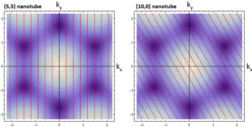
Figure 6. Contour plot of the E k( )
relationship of graphene showing the cutting lines (red) imposed by the periodic boundary condition, turning the 2D graphene system into a 1D CNT. The examples shown here are for a (5,5) metallic and a (10,0) semiconducting nanotube.
17
Thus, the band structure of CNTs is derived from that of graphene, plus the boundary condition. This results in the quantization of the graphene states shown in Figure 6, with red lines showing the allowed states. For a (5,5) nanotube the K points fall on the red lines, meaning that it has states around the Fermi level. In the case of the (10,0) nanotube, none of the allowed K points cross the allowed states, resulting in a band gap. The nanotube bands can be calculated using this so called zone folding method [52] in the tight binding approximation [55]. These bands are plotted in Figure 7 for both nanotubes.
Figure 7. Bands and density of states (DOS) for a (5,5) metallic (a, b) and a (10,0) semiconducting nanotube (c, d), calculated using the tight binding approximation for s0 = 0 [55]. The bands are plotted along the k
vector parallel to the tube axis. The (10,0) semiconducting nanotube has a band gap of roughly 1 eV. Van Hove singularities appear in the DOS, at the minimum and maximum points of the tube bands. The structural model of the (5,5) armchair (top) and (10,0) zigzag (bottom) nanotubes can be seen on the right.
A general rule is that a nanotube is metallic if the chiral indexes n and m obey the following relation: 2n+ =m 3p, where p is an integer [52]. In the case of semiconducting nanotubes,
18
the band gap scales inversely with the tube diameter: Egap =(2 / 3)γ0a d/ t, where dt is the CNT diameter. The density of states of nanotubes shows a series of sharp peaks, so called Van Hove singularities [56]. These peaks determine the charge transport properties and the transitions between these states, the optical properties of CNTs [57].
The simple picture used above to describe the band structure can be further refined by taking into account the curvature of the nanotubes, where the mixing of the sp and π bonds modifies the above description. This effect is significant in the case of small diameter nanotubes [58, 59].
Another type of nanotube, are the so called multiwalled CNTs (MWCNT). In the case of a MWCNT individual, concentric graphene tubes are stacked one into the other (Figure 8).
Figure 8. A multiwalled carbon nanotube composed of single walled tubes of different chiralities. The interlayer spacing of the nanotubes is roughly the same as the layer to layer spacing of graphite. (Image rendered using nanohub.org [55])
It was MWCNTs that were described in the landmark paper by Iijima [14], using TEM to reveal the structure of these tubes (Figure 9). The discovery of SWCNTs came later in 1993 by two teams publishing in the same issue of the journal Nature [60, 61]. The interlayer spacing between the concentric nanotube shells is slightly larger than the interlayer spacing in graphite: 0.335 nm and its exact value depends on the chiral indices of the individual tubes forming the MWCNT, having an average value of 0.339 nm [62]. Another important feature of MWCNTs is that while SWCNTs can have diameters of only up to 2 nm,
19
multiwalled tubes can have diameters in the range of tens of nanometers and in some cases even more than 100 nm [63, 64]. Since graphite can be considered a MWCNT of infinite diameter, such very large diameter nanotubes behave much like graphite under certain circumstances.
Figure 9. Transmission electron microscopy (TEM) image of MWCNTs published by S. Iijima. The individual nanotube walls can be resolved by electron microscopy. Reproduced from ref. [14]
1.3. Production of carbon nanotubes and graphene 1.3.1. Carbon nanotubes
The method used by Iijima [14] and adopted by other early investigators was that of arc discharge between two graphite electrodes in an inert atmosphere [14, 60, 65, 66, 68]. To prepare SWCNTs, the graphite electrodes are loaded with a metallic catalyst (Fe, Co, Ni, Y, Mo) and in the high temperature plasma that forms in the electric arc, the graphite electrodes are vaporized along with the catalyst and the carbon condenses in the form of nanotubes. In later years the laser ablation method used to produce fullerenes [13] was adapted for the production of CNTs, mostly SWCNT [65, 66]. Successful as these methods may be, none of them can be used to produce CNTs in the large scales required by the modern CNT industry. The breakthrough technique that enabled CNTs to become an industrial material was a route that involved chemical vapor deposition (CVD).
20
The catalytic decomposition of hydrocarbons was used well before the discovery of CNTs for the production of certain kinds of carbon fiber [67] and it was Yakaman et al. that successfully used this technique to obtain CNTs [68]. This synthesis route makes possible the production of CNTs in a continuous manner and enables a kind of control over the nanotube parameters that other techniques do not offer [23, 69, 70, 71], including: the patterned growth of nanotubes [72]; the growth of centimeter long nanotubes [73]; doped CNTs [74], etc. Since CVD was used to prepare the nanotubes investigated in this work, I will introduce this method in more detail.
CVD growth involves the use of a transition metal nanoparticles as catalyst (usually Fe, Ni, Co, Mo) either in the pure form or as an alloy [75, 76]. This catalyst is introduced into a furnace as a metal-organic precursor or supported on a substrate in the form of metallic nanoparticles and heated to a temperature in the range of 500oC to 1200oC [77]. Carbon nanotube synthesis begins on the nanoparticles if a suitable source of carbon is introduced.
The carbon source is usually a hydrocarbon (methane, ethane, ethanol, benzene, etc) or CO as in the case of the HiPCO method [78]. The hydrocarbon gas is catalytically decomposed at the metallic nanoparticles, it diffuses through the bulk or surface of the nanoparticle finally forming graphitic shells. The graphitic material precipitating on the catalyst nanoparticle follows the morphology of the particle, forming the graphitic cylinders of single- or multiwalled nanotubes (Figure 10).
Figure 10. (a) Schematic of the CVD nanotube growth process. (b) The role of metallic nanoparticles during MWCNT growth.
21
The reaction mechanism briefly described above is much more complex and is still not completely understood [77]. The complete process involves the subtle interplay between nanoparticle dynamics, surface and bulk diffusion of carbon and the energetics of the metal surface – graphene – gas phase system.
1.3.2. Graphene
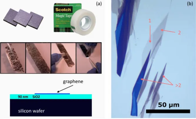
The method by which single layer graphene flakes were isolated from bulk graphite for the first time is still the most widely used technique to obtain graphene layers for research purposes. In 2004 Novoselov et al. used ordinary “scotch” tape to peel off layers of graphite from HOPG, a highly crystalline form of graphite produced synthetically [5]. This so called micromechanical cleaving technique consists of repeated pealing of the graphite crystallites stuck to the scotch tape, during which ever thinner crystals are produced on the tape surface. The graphite crystals separate very easily because the individual graphene planes in graphite are bound only by weak Van der Waals forces. After pealing, the tape is pressed against the surface of a silicon wafer having either a 90 or 300 nm of SiO2 capping layer.
While the tape is removed from the surface of the wafer the crystallites sticking to the SiO2
surface cleave one last time and the result is an assortment of graphite crystals with varying thicknesses on the SiO2 (Figure 11b). One of the most important factors that enabled the discovery of single layer graphite among these crystallites is that even graphene, not to mention bilayer graphene, can be seen with a conventional optical microscope on top of a wafer with carefully chosen SiO2 thickness. This effect arises because graphene has a certain opacity and it also adds to the optical path of the light traversing the SiO2 capping layer [79].
Together, these effects are enough to give graphene a well discernible contrast in an optical microscope.
The graphene samples investigated in this work have all been prepared by the method described above. The reason this technique is preferred for many research purposes is because of the ease of preparation, the ability to prepare graphene flakes with large lateral size (even up to 1 mm) and that the graphene layers are nearly free of crystal defects.
Nevertheless, micromechanical cleaving is not the only method available.
Another important graphene preparation technique, also published in 2004 [39], involves the formation of graphene layers on either the silicon or carbon face of SiC single crystals.
22
The SiC wafer is heated to temperatures in the 1200-1400oC range allowing the removal of surface silicon, leaving a carbon rich phase which forms graphene layers at these high temperatures. This process is ideally suited for future electronics purposes, because the graphene covers the entire surface of the SiC wafer and the substrate. However, the graphene prepared this way has more crystal defects than cleaved graphene [80].
Figure 11. (a) Process of preparing graphene. In this “top-down” process, some highly crystalline graphite, like HOPG is repeatedly pealed using sticky tape. (b) Optical microscopy image of single layer graphene on 90 nm thick SiO2. Single, bi- and multi layered graphite is highlighted by the red arrows.
Similarly to the case of CNTs, CVD methods have evolved to becoming one of the most important methods of graphene preparation, enabling the growth of graphene samples of macroscopic size [81]. Especially important is the growth of graphene layers on copper, pioneered by the group of Rodney S. Ruoff [82]. During this process a flow of hydrocarbons (usually methane) at low partial pressure is passed above a transition metal poly- or single crystal, heated to ~1000oC. Depending on the CVD parameters (pressure, temperature, cooling rate) single or multilayer graphene is deposited on the metal surface, which can be etched away and the graphene transferred to arbitrary substrates [81, 82]. Using this growth process, the size of the graphene is limited only by the size of the metal substrate, but it is important to mention that the graphene prepared this way is not a single crystal. During
23
growth multiple nucleation sites form on the metal surface, making the graphene a patchwork of grains a few 100 nm to a few microns in size [ 83]. Controlling this microstructure of CVD grown graphene remains a challenge.
1.4. Tailoring the electronic properties of carbon nanotubes and graphene Since 2004 and the milestone papers describing some of the exciting properties of graphene [5, 36, 38, 39], the research into its basic properties has expanded in an almost exponential manner (Figure 2) [84]. The industrial use of graphene seems to be following suit, with some niche applications almost ready for market, most notably the use of graphene in displays, due to the fact that graphene has begun to match and in some sense to outperform indium- tin-oxide as a transparent electrode material [81]. But one of the biggest potentials for applications lies in exploiting the superior electronic properties of graphene in electronics.
For example: it has high carrier mobility, for a wide interval of the value of the chemical potential [7, 8]; large charge carrier saturation speed [85]; high thermal conductivity [86]
and in transistors: the smallest possible (one atom thick) channel thickness [87]; flexibility [81], etc. These properties make graphene based field effect transistors (FET) a candidate for future electronics applications. From among these properties, large charge carrier mobility is required for high speed devices, while high thermal conductivity 30-50 W cm-1 K-1 (about 10x the value for copper) aides heat dissipation in devices [87]. In recent years, very promising radio frequency transistors have been prepared, which use graphene as a channel material.
These devices have a cut-off frequency (the frequency at which the transistor is still usable in RF applications) of 100 GHz [88], exceeding the performance of Si based, and approaching that of GaAs based high electron mobility transistors of similar gate lengths [87].
On the other hand, despite the proposals made for graphene based logic FET devices [89], this kind of application still eludes us, due to the high on/off current ratios (104-107) required for such applications. The crux of the problems is the lack of a band gap in graphene.
However this “deficiency” can be addressed by various means of “band gap tailoring“ [8].
In the case of CNTs the lack of a band gap is seemingly not a problem, as one of the interesting properties of nanotubes is that their electronic structure can be tuned by changing the chirality of the nanotubes. The band gap can vary from a metallic state to large
24
gap values in the 1 eV range. However, “tuning” is a misnomer. To be able to tune the properties, one would need to be able to synthesize CNTs with a specific chirality, or be able to separate a single chirality from among many in a sample. Research effort in this direction has begun to bear fruit [24, 25] but there are other, depending on application, more convenient routes to tailor the properties of CNTs through the attachment of chemical groups to the nanotube sidewall.
1.4.1. Carbon nanotube functionalization
The chemical modification of the nanotube sidewalls enables the tuning of the interaction of the tubes with their environment and tailoring of the nanotube properties [90, 91], while allowing researchers to employ the vast possibilities offered by chemical methods in tackling these problems. The attachment of chemical groups to the nanotube sidewalls (functionalization) can be used to alter the nanotube electronic properties [90, 92, 93, 94, 95, 96] and may be used to tune the interaction of the nanotubes with their surrounding [3, 97] and each other, for example to achieve their self assembly into device architectures [98].
Various forms of functionalization exist, depending on the nature of the chemical bond between nanotube and chemical group [90], for example physisorption of molecules can have influence on the CNT properties [99]. However, in the present work I explore the properties of CNTs, which have functional groups attached to their sidewalls by covalent bonds. As such, I introduce these systems in more detail.
The addition of functional groups to the nanotubes usually takes place at defect sites in the CNTs or at the end caps. This is due to the lower activation energy for chemical reactions at defect sites (vacancy, non hexagonal arrangement of C atoms, etc.). The defect concentration on CNTs is in the order of 1-3% of the carbon atoms [100], so the functional group concentration will have a similar value. Only very harsh conditions, such as fluorination, allow the addition of chemical species directly to the sidewalls [101]. Thus, usually before the functionalization reactions are implemented, further defect sites are generated by oxidation [ 102]. After defect creation the nanotube sidewall can be functionalized by a variety of chemical groups [91], a very common option being carboxylic groups, which can be introduced by exposing the CNTs to nitric acid (Figure 12) [91, 100].
25
Figure 12. A flow-chart of CNT functionalization. A usual route is the introduction of defects into the nanotube sidewall and ends (red circles). This is followed be the addition of chemical species to the as obtained defect sites, in this case carboxyl groups, using nitric acid treatment.
After the addition of the functional groups (in our case carboxylic groups), a wide range of chemical modifications can be performed on them, allowing the coupling of other molecules by covalent bonds [76, 90, 91, 102, 103, 104].
The changes induced by functionalization in the nanotube electronic structure is a strong function of functional group concentration and type. At very high functionalization degrees and random distribution of functional groups, the translational symmetry of the nanotube will be broken and we can no longer talk about the CNT band structure, as such. If a high concentration of functional groups are arranged in an ordered and periodic fashion on the nanotube sidewall the band structure changes dramatically [105]. However, this kind of ordering has not yet been achieved experimentally and the distribution of functional groups in samples studied to date can be considered random [90]. At low functional group concentrations discussed in this work (a few % of the C atoms) the influence of the functional groups can be considered as a perturbation of the nanotube band structure. This perturbation manifests itself in many forms. The addition of functional groups can change in the Fermi level of the nanotube, often referred to as doping, for example in the case of the addition of dichlorocarbene [94] or the physisorption of nitric acid on the tube sidewall [99].
During functionalization, as in the specific case of carboxyl group addition, the sp2 carbon in the tube sidewall transforms into a sp3 type atom. This change in the hybridization has significant influence on the charge transport properties of the CNT [95]. These effects are a kind of global influence, effecting the whole of the nanotube sample. More localized types of
26
perturbation are changes induced by specific chemical groups in the local electronic structure of the nanotube. The addition of functional groups creates additional states in the CNT band structure. Such changes are specific to the kind of functional group producing them, and are localized around the chemical group [92] (Figure 13).
Figure 13. (Left) States induced in a (10,0) nanotube by carboxyl and hydroxyl groups, calculated from first principles. (Right) Iso plot of the impurity wave function induced by a carboxyl group. Reproduced from ref. 92.
Other changes in the CNT band structure as a result of functionalization are the observation of band gap opening in the case of metallic nanotubes and a suppression of the optical transitions between the nearest van Hove singularities [94]. Of course the ultimate goal of CNT functionalization is the exploitation of the nanotubes with tailor made properties in various applications. In Table 1 a list of such possible applications is given.
Characterization of the functional groups and the changes in the CNT electronic structure are predominantly investigated by optical spectroscopic methods [90]. Part of my work has been focused on enabling the visualization and characterization of functional sites on CNTs by scanning probe methods, specifically scanning tunneling microscopy (STM), which yield significant new information and complement existing spectroscopic techniques. In the chapters to come I will describe advantages of STM and new insights gained.
27
Table 1. Potential applications of functionalized CNTs, adapted from ref. 91.
(Potential) Application Function of the covalently bonded chemical group
Nanostructured electronic devices Local modification of the electronic band
structure
Mechanically reinforced composites Chemical coupling with a matrix
(Bio-) chemical sensors Selective recognition of analyte molecules
Catalyst supports Anchoring of molecules or metal
nanoparticles Chemically sensitive tips for scanning probe
microscopy Selective chemical interaction with surfaces
Field emission Reduction of the work function for electrons
at the tube ends
Artificial muscles Mechanical stabilization of nanotube films
through covalent cross-linking
Controlled drug release Biocompatibility; recognition of biological
fingerprints
Directed cell growth on surfaces Specific interactions with cell surfaces
Pharmacology Enzyme inhibition or blocking of ionic
channels in the cell
1.4.2. Graphene nanoribbons and other graphene nanostructures
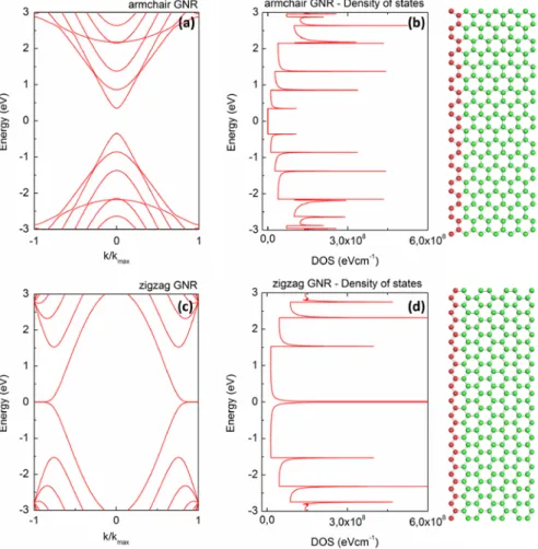
One of the most interesting features of graphene is the rich physics encountered when various nanostructures of graphene are considered. One type of nanostructuring was considered even before the discovery of exfoliated graphene. In 1996 Nakada et al. have theoretically explored the properties of graphene strips of a few nanometers width [106]
(Figure 14). This lateral confinement has a similar effect on the electrons as the periodic
28
boundary condition in the case of CNTs. In a first approximation, the bands of such a graphene nanoribbon (GNR) can be obtained by applying the same kind of zone folding on the graphene band structure as in the case of CNTs and using the tight binding approximation [55, 106, 107] (Figure 14).
Figure 14. Band structure plotted along the wave vector parallel to the GNR axis (a, c) and density of states (b, d) for a armchair (top) and zigzag (bottom) type GNR. Structural models of the ribbons can be seen on the right.
The bands are calculated using the tight binding approximation [55], neglecting the edge states of the ribbons.
This particular armchair GNR has a band gap of almost 0.7 eV. A peculiar feature of the zigzag GNR bands is the flat bands at the Fermi level, which result in a sharp peak in the DOS.
We can analyze the case of GNRs with one of the two most stable edge geometries, either zigzag or armchair type. Analogous to the case of CNTs the bands of GNRs depend very strongly on the crystallographic orientation of the GNRs, with zigzag edged GNRs being metallic in character and some armchair type GNRs having a band gap. The size of this band gap scales roughly as a power law with the width of the nanoribbon (roughly 1/width).
Zigzag edged GNRs have states all the way through the Fermi energy, making them metallic.
29
They also have a very flat band right at the Fermi energy, which results in a sharp peak in the density of states (Figure 14). This state is localized on the zigzag edge [106] and can be observed in scanning tunneling microscopy (STM) images of graphite edges [108]. The nanoribbons studied here are considered to have hydrogen terminated edge atoms.
Observing that atoms at the edges of the nanoribbons do not have three other neighbors as in an infinite graphene crystal, we realize that in the above description the periodic boundary condition imposed on the graphene has no real physical meaning. Thus, we need to take into account the perturbation introduced by the edges. Son et al. have calculated the bands of graphene nanoribbons using first principles [109], including these edge effects.
These calculations also reproduce the particular edge state of zigzag nanoribbons, but as it turns out these ribbons also have a minute band gap (Figure 15b). The band gap arises if the spin degrees of freedom are taken into account, with a predicted ferromagnetic state at the zigzag edge and antiferromagnetic ordering between the opposing nanoribbon edges.
Figure 15. (a) Band gap of armchair type GNRs calculated from first principles. (b) Taking into account edge effects, even zigzag GNRs display a small band gap. Images adapted from ref. 109
Later theoretical investigation has shown that the magnetic states at the zigzag GNR edges can grant the nanoribbon a half metallic behavior if an electric field parallel to the GNR strip is applied [110]. Half metallic in the sense that the nanoribbon behaves like a metal for one spin state and as an insulator for the other. This prediction makes zigzag edged GNRs a possible candidate for use in spintronics devices, where usually d band metals are thought to be usable and not carbon, which has no intrinsic magnetism.
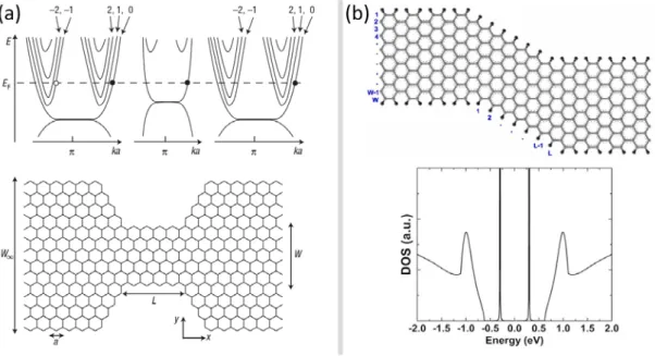
Beyond the spin properties of GNRs other, more exotic behavior is predicted for example in a kind of graphene nanoribbon structure seen in Figure 16a. Such a device would only admit charges from one K valley of graphene to pass through the narrow ribbon region. This would
30
enable the use of the valley degree of freedom in graphene for information processing, a kind of valley-tronics analogous to spintronics [111]. Going a step further, if we combine armchair and zigzag GNR structures into more complex systems, equally interesting properties can result, for example a quantum dot-like system in a zigzag nanoribbon device with armchair GNR leads (Figure 16b) [112].
Figure 16. (a) A „valley-filter” realized in a graphene zigzag edged constriction, where the device only lets electrons from one K valley through (bands of the leads and constriction shown on the top). (b) A z shaped constriction consisting of a zigzag GNR section, with armchair GNR leads. The zigzag region shows quantum dot-like states. Image (a) reproduced from ref. 111 and (b) from ref. 112.
The predicted behavior of all the above examples, not to mention the properties of GNRs in general, rest on the assumption that the GNRs have atomically smooth edges, as shown in Figure 14. As is the case with all nanosized systems, graphene is very susceptible to the effects and interactions occurring at the surface atoms. In the case of graphene, all atoms are at the nanostructure surface or edges, thus the properties of GNRs, or of other graphene nanostructures will depend strongly on the kind of environment (supporting substrate, ambient, etc.) it is subjected to and the specific configuration of edge atoms. Real samples of GNRs and graphene will have a certain concentration of defects (vacancies, pentagon- heptagon pairs, disorder at the edges, etc.), which have a significant influence on the electronic structure and charge transport properties. It has been shown theoretically that the degree of edge functionalization [113, 114], not to mention the type of functionalizing radical [115] can have drastic effects on the charge transport mechanism [116,117] and
31
nanoribbon structure [118, 119]. This is one of the reasons, why the strong difference between zigzag and armchair nanoribbons, resulting from their different edge geometries, has not been detected in real systems yet [120, 121, 122]. Conventional routes of obtaining nanoribbons produce ribbons with highly disordered edges, the result of which is that the nanoribbon properties will not be dominated by the specific physics of armchair or zigzag edge terminations, but the degree of disorder [120, 122], although there have been some hints at edge specific behavior in zigzag edged graphene quantum dots [123] and the observation of possible quantum confinement effects [124].
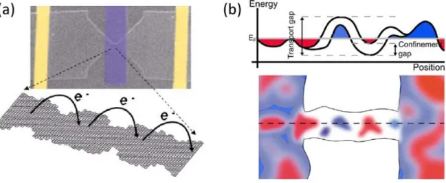
It has been shown that in graphene nanoribbons obtained by traditional electron beam lithographic methods one finds a band gap, but this gap is not the result of the lateral confinement of the graphene [120]. It is a so called transport gap, being the result of various processes induced by disorder. Charge transport in this gap region is determined by thermally exited hopping between localized states [121]. The disorder responsible for this kind of behavior is either edge disorder in the GNR [121, 122] or charge inhomogeneity in the supporting SiO2 substrate [125, 126]; it is most likely an interplay of both these effects (Figure 17).
Figure 17. (a) A GNR produced by electron beam lithography. Due to edge disorder, the ribbon can be considered as a series of quantum dots, transport can be considered as a hopping of charge carriers between these. (b) Such quantum dot-like states can form as a result of charged impurities present in the SiO2 substrate.
Images reproduced from ref. 122 and 126.
32
Beyond charge transport experiments, optical means of differentiating between graphene’s zigzag and armchair edges has proven to be a difficult endeavor. Inelastic light scattering has been proposed as a means to differentiate between the zigzag and armchair edges of graphene flakes, with a particular peak in the Raman spectra of graphene predicted to be localized on armchair edges [127]. According to theoretical considerations, this so called D peak, at 1350 cm-1, should be absent on the zigzag edges. However, it has proven difficult to find such a marked difference in real graphene samples [127].
As mentioned before, the planar structure of graphene makes this material ideal for patterning it on the nanoscale. The breathtakingly fast evolution of research into graphene growth, mainly by the CVD method [81], has made possible the preparation of graphene samples of arbitrary size. Such sample production, combined with the right patterning tools could be used to tailor the graphene sheet into functional nanostructures, even whole electronic circuits [128]. However, based on the experimental results reviewed above, it is clear that observing the predicted edge specific physical phenomena in graphene nanostructures remains a challenge. The preparation of graphene nanostructures and the validation of theoretical predictions regarding specific effects arising from zigzag and armchair edges is one of the major goals of graphene research. In this thesis I describe a lithographic procedure, which allows the creation of zigzag edged graphene nanostructures and nanoribbons [T129*], opening up a new sample preparation route, bringing us one step closer the experimental validation of the predicted physical phenomena in zigzag type graphene nanostructures.
1.4.3. Preparation of GNRs
One method of graphene patterning has been used since the beginning of graphene research to pattern it into the “Hall-bar” geometries used to explore its peculiar magneto- transport properties [36, 38]. This technique relies on the creation of a polymer mask on top of graphene, by spin coating PMMA (polymethyl methacrylate) and exposing certain regions of the mask with an electron beam, making the polymer in the exposed regions selectively dissolve in a solvent. Such a mask can be used to etch certain regions of the graphene flake
* For the purpose of clarity the letter “T” is added in front of citations to articles used as a basis for writing the thesis points of the dissertation.
33
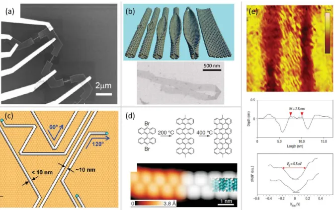
and to deposit metal contacts to the graphene structures defined this way. This is by far the most widely used technique to prepare nanoribbons [120] (Figure 18a). On its own, this technique cannot produce graphene nanostructures with crystallographically well defined edges, because the scanning electron microscope used to expose the polymer film does not have the desired lateral resolution. Furthermore, due to the oxygen plasma etching used, the edges of the graphene are highly disordered [122].
One technique which looked promising is the etching of CNTs along the tube axis in such a way as to obtain GNRs [130, 131] (Figure 18b). This may be a promising way to prepare GNRs in large quantities, but on closer inspection, it becomes clear that the technique inherits the problems plaguing CNTs. Namely that the diameter of CNTs cannot be controlled precisely. This is because the width of the GNRs is determined by the diameter of the nanotube we’re “unzipping”. Furthermore, the crystallographic orientation of the GNR edges is not known, or cannot be controlled [131]. There are only some hints that the GNR edge obtained using certain techniques [130] is predominantly of the zigzag type [T132].
The etching of graphite and graphene layers by metallic nanoparticles is also a promising
“nanomachining” process [133]. Metallic nanoparticles (Ni, Fe, Co) are deposited on graphene flakes and annealed at ~500oC, usually in a flow of Ar and H2. During this treatment the metallic nanoparticles cut trenches into the graphene, with well defined crystallographic orientation (Figure 18c). There is evidence that at least in certain cases the trench edges have zigzag orientation [134].
One method which was able to successfully pattern GNRs with a well defined crystallographic orientation and width is STM lithography [135]. The STM tip is scanned over the surface, with a tip – sample bias voltage higher than that used for imaging and as a result very narrow trenches can be carved into the surface of graphite. Crystallographic orientation control is achieved because the STM is able to resolve the atomic structure of the surface.
Very narrow nanoribbons (2.5 nm in Figure 18e) can be prepared due to the high precision with which the STM tip can positioned over the surface. One drawback is that the GNRs cannot be prepared on an insulating surface.
34
Figure 18. Methods of GNR preparation. (a) electron beam lithography; (b) „unzipping” of CNTs; (c) etching by metallic nanoparticles; (d) self assembly of aromatic molecules. (e) An armchair edged GNR patterned by STM lithography. Images adapted from ref.: 120, 130, 133, 135 and 136.
All the methods and processes of obtaining graphene nanostructures rely on some kind of nanostructuring of large area graphene layers. Alongside these top-down approaches, bottom-up processes, such as the self assembly of large aromatic molecules has been successfully applied to produce nanoribbons [136]. Chemically assembling GNRs from large organic molecules has the advantage of allowing the creation of very narrow nanoribbons (Figure 18d) , which have crystallographically well defined edges. However, the control over the width and length of the GNR and the controlled patterning or placement on a substrate has not been achieved yet. Furthermore, such self assembled graphene structures are usually grown on a metal substrate, which means that their electronic structure may be seriously perturbed by the vicinity of the metal. Table 2 compares the properties of the graphene patterning techniques discussed. These techniques are the ones most investigated and most relevant. However, over the years many different graphene patterning techniques have been developed, far too many for this work to give a completely accurate account of the field [137].

![Figure 7. Bands and density of states (DOS) for a (5,5) metallic (a, b) and a (10,0) semiconducting nanotube (c, d), calculated using the tight binding approximation for s 0 = 0 [55]](https://thumb-eu.123doks.com/thumbv2/9dokorg/1310187.105425/17.893.203.730.359.898/figure-density-metallic-semiconducting-nanotube-calculated-binding-approximation.webp)