Compressed sensing in FET based terahertz imaging
Gergelyi Domonkos
A thesis submitted for the Doctor of Philosophy
Pázmány Péter Catholic University
Faculty of Information Technology and Bionics Roska Tamás Doctoral School of Sciences and Technology
Supervisor Péter Földesy, Ph.D.
Budapest, 2014
- 2 -
T É M A V E Z E T Ő I N Y I L A T K O Z A T O K
1. PUBLIKÁCIÓS TELJESÍTMÉNY
Alul írott Dr. Földesy Péter Témavezető nyilatkozom, hogy Gergelyi Domonkos doktorjelölt publikációs teljesítménye megfelel a doktori (PhD) fokozatszerzési eljárás előfeltételeként a Tudományterületi Doktori és Habilitációs Tanács által támasztott követelményeknek.
2. PhD disszertáció
Alul írott Dr. Földesy Péter Témavezető nyilatkozom, hogy Gergelyi Domonkos doktorjelölt benyújtott doktori munkájában meghatározott téma tudományosan értelmezhető, hiteles adatokat tartalmaz, az abban foglalt tudományos eredmények a jelölt saját tudományos eredményei, az értekezés megfelel a PPKE PhD szabályzat, és a MMT DI SzMSz előírásainak.
A PhD disszertáció nyilvános vitára történő benyújtását támogatom.
2015. Május 13.
………
Dr. Földesy Péter, PhD, Egyetemi docens, PPKE-ITK
- 3 -
Table of Contents
1 Introduction ... 8
1.1 Introduction of the field ... 8
1.1.1 Terahertz sensing ... 8
1.1.2 Terahertz spectroscopy ... 8
1.1.3 Terahertz imaging ... 9
1.2 Compressed sensing ... 11
1.3 Related work in the application of CS ... 15
1.3.1 SLMs in the THz domain ... 15
1.3.2 CS capable focal plane arrays for viewable light ... 16
2 The research project... 17
2.1 Aims of the project ... 17
2.2 The goals of my research work - problems to solve ... 20
2.3 Setup ... 20
2.3.1 Source ... 20
2.3.2 Quasi optical setups ... 22
2.3.3 Antenna coupled FET detectors... 23
2.3.1 A/D conversion ... 29
2.4 180 nm Serially connected sensor array ... 29
3 Noise performance of compressed sensing based detectors ... 40
3.1 Motivation ... 40
3.1.1 The aspect of implementation and system integration... 40
3.1.2 Considerations on the setup ... 41
3.2 Methods ... 42
3.2.1 General approach ... 42
3.2.2 Cross validation for increasing SNR ... 44
3.2.3 Figure of merit ... 44
3.2.4 Noise reduction basics ... 46
3.2.5 Assumptions ... 47
3.2.6 Noise model of terahertz FET detectors ... 47
3.2.7 Detector response ... 48
3.2.8 Modeling of the system ... 49
3.3 Results and conclusions ... 49
Thesis 1 [SNR enhancement of imaging systems with compressed sensing] ... 49
Thesis 2 [Relation of CS to physical implementations of terahertz imaging systems – holistic approach] ... 55
3.3.1 Passive gain of a CS architecture... 55
3.3.2 Considerations on the implementation ... 60
3.4 Related problems ... 68
- 4 -
3.4.1 The problem of the optical setup ... 68
3.4.2 Raster scanning on non-uniform grids ... 68
3.4.3 Depth of sensing ... 69
4 Experimental validation - Measurements ... 71
4.1 Targeted diagnostic usage ... 71
4.1.1 Water concentration ... 72
4.1.2 Ex-vivo investigation of human tissue ... 72
4.2 Imaging of phantoms and test objects ... 74
5 Fields of application ... 77
6 Summary ... 78
7 Acknowledgements ... 80
8 Author’s publications ... 81
9 References ... 82
Structure of the work
After a short introduction of the field in section 1, I summarize the long-term aims of the terahertz research group at the Computational Optical Sensing and Processing Laboratory (COSPL) that drove the work during the past years. I continue with describing the utilized setup giving also an insight to the process of the project that helps to clearly position my own contribution.
The third section constitutes the core of this thesis starting with the general approach of my investigations and an overview of the used methods. Then, I present the scientific results of my work.
In the next part, a collection of some measurements brings the work closer to the reader demonstrating the technological problems and challenges of terahertz sensing. I close the work by outlining the conclusions and discussing the fields of application.
For several sections of the document, I utilized the text of my publications word by word as concise description of a number of topics (especially [2]).
- 5 -
List of Abbreviations and Symbols
2DEG Two Dimensional Electron Gas ADC Analog to Digital Converter AMC Amplifier Multiplier Chain
BP Basis Pursuit
BPDN Basis Pursuit Denoising
BSIMv3 A physics based circuit simulation model of a MOSFET developed by the UC Berkeley Device Group; version 3.0; first industry-wide standard, 1996
CCD Charge-coupled Device
CMOS Complementary Metal Oxide Semiconductor
CoSa Compressed Sampling
CoSaMP An optimal CS reconstruction algorithm regarding, the reconstruction error, and the number of measurements
COSPL Computational Optical Sensing and Processing Laboratory of the ICSC
CS Compressed Sensing
CV Cross-validation
CW Continuous Wave
DAQ Data Acquisition
DMD Digital Micromirror Device FET Field Effect Transistor
FFT Fast Fourier Transform
FPA Focal Plane Array
ICSC – HAS Institute for Computer Science and Control of the Hungarian Academy of Sciences
IMPATT diode IMPact ionization Avalance Transit-Time diode; high power semiconductor diode; oscillator, amplifier in the range 3-100 GHz
ITU International Telecommunications Union
LC Liquid crystal
LNA Low Noise Amplifier
MOS Metal Oxide Semiconductor
NA Numerical Aperture
NEP Noise Equivalent Power
NF Noise Figure
OMP Orthogonal Matching Pursuit PSD Phase Sensitive Detection
SLM Spatial Light Modulator
SNR Signal to Noise Ratio
- 6 -
SoC System on Chip
THF Tremendously High Frequency band (ITU) or THz; 300 GHz – 3 THz THz Terahertz; frequency of 1012 Hz
VLSI Very Large Scale Integration
YIG Yttrium Iron Garnet
ρ-Si High resistivity silicon
---
tint It is used if no capacitance is considered inside the pixel, only integration after the LNA; therefore, tint= tint2
tint1 In-pixel integration ratio (referenced to 0.5s – that is the base of NEP calculation by definition); also known as the relative integration time; this assumes an integrating capacitance inside the pixel (below the antenna) – hence, very limited – we assume no in pixel capacitance
tint2 Relative integration time after the LNA (tint2 = (int. time in sec)/0.5 sec);
otherwise the same as the in-pixel integration ratio or relative int. time 𝑀𝑝𝑐 Number of needed CS measurements per cluster (Mpc < Npc) to be able to
reconstruct all, Npc number of pixel values within the cluster
𝑁𝑐𝑠 The average number of active pixels in the CS patterns (within the integration time)
𝑁𝑝𝑐 Number of pixels per cluster (pixel cluster size) 𝑃𝑡𝑜𝑡𝑎𝑙 Total noise power of a detector transistor
𝑇0 290 K
𝑓𝑠𝑚𝑎𝑥 The theoretical, summed maximum sampling frequency of all A/D unit working as a single unit in an ideal, time interleaved fashion
𝑓𝑠 Sampling frequency of the A/D converters (we assume the total resources available for A/D is limited by the chip area; 𝑓𝑠= 𝑓𝑠𝑚𝑎𝑥/𝑟) 𝑓𝑠𝑚 The modulation frequency of the source; it is used for the lock-in
detection that is the assumed basic measurement scheme fps Acquisition speed; frame per second
L0 norm The “sparsity” of a vector; see section 1.2 for details
L1 norm The “absolute value norm” of a vector; see section 1.2 for details
λ Wavelength
𝐵 Bandwidth of the measurement (usually determined by the lock-in amplifier – 𝑓𝑠𝑚)
𝑀 Number of needed CS measurements to reconstruct the image; at an estimated average compression: M ≈ 4s log(N), if the image is s-sparse; it is for the whole imagein contrast to 𝑀𝑝𝑐 that considers only a small cluster 𝑁 Number of pixels in the imager
𝑁𝐹 Noise figure of the LNA
- 7 -
𝑆 Sample count (see definition in section 3.3.1) 𝑘 Number of pixel clusters
𝑟 Number of A/D converters; we assume ideal resource sharing; 𝑟 = 𝑘 𝒙 The signal/image to be measured, rearranged in a vector form (column
wise repacking, where the columns get below each other)
𝒚 The measurement vector; 𝒚 ∈ ℝ𝐌 – it stores a single value for each measurement
𝛟 Measurement matrix; consisting of the patterns as its rows; 𝛟 ∈ ℝ𝐌×𝐍 𝜂 Efficiency of summation at the compressed sampling (here ~0.81);
summing the unity signal of 𝑁 pixels, results in a signal amplitude: 𝑁𝜂
- 8 -
1 I NTRODUCTION
1.1 Introduction of the field
1.1.1 Terahertz sensing
Terahertz science is a relatively new, fast developing research area that covers the electromagnetic spectrum from 0.1 THz to 30 THz. Its main topics cover the info- communication field and sensing in general. Astronomy was its first application field, where imaging started. Since then, surveillance applications came to everyday use to help security screening in avionics. The non-destructing imaging capabilities proved its usefulness for historians as well, by giving insight to ancient, closed crocks. Surface inspection, material characterization and biological observation are also in the forefront. Spectroscopy developed a lot since the beginnings; the new techniques provide much more information about molecular fine structures.
Non-invasive inspection of cell cultures and thick excisions of various tissues paved the way for the first clinical in-vivo application: breast cancer diagnosis [2].
1.1.2 Terahertz spectroscopy
The 0.1 THz to 30 THz frequency spectrum covers the 0.4∙10-3 – 120∙10-3 eV energy range.
Thus, the electromagnetic field affects rotational and vibrating modes of the molecules making it applicable to gather information about the molecular structure of the objects and to characterize compounds via recording such features.
Investigations in this field started quite early in the 60s and 70s [3]. Since then, the aim has not changed much yet: increase accuracy further and further to create ever finer spectral traces and determine the observed molecular structure more faithfully.
With development of the technology many other subfield emerged and lower part of the spectrum, the THF band became more easily measurable (for instance the Schottky diode sources and detectors of the Bell Labs got widespread accessible).
Several methods are available to unveil spectral patterns of substances. Complementary or alternative approaches might provide the same spectral features (peaks) with different relative amplitudes, when the intensity values result from variant underlying processes. By way of example Raman spectroscopy, infrared spectroscopy and incoherent inelastic neutron scattering based crystallography relay on fundamentally different interactions.
However, there are many equivalent techniques giving the same results at different speed, precision and complexity.
- 9 - 1.1.2.1 Time domain spectroscopy (TDS)
This proven technique is popular in the field of terahertz inspection, where a non-linear crystal such as ZnTe or LiNbO3 converts the power of a pulsed laser source to terahertz radiation. The laser beam is divided to object and reference beams to allow the reference beam gating the detector through a delay line. This fine controlled delayed gating signal makes possible to scan the generated THz pulse in an iterative manner. All techniques utilizing such a conversion have advantage at in-vivo measurements as the probe consisting only the converter crystal and the detector can be “powered” through flexible, fiber cables. This makes the setup compact and ergonomic allowing probing arbitrary parts of the body in a diagnostic setup. The head of the probe can be relatively small with a silicon lens at its tip that couples the terahertz radiation from the crystal into the skin on a short traveling path and vice versa, gathering the backscattered signal from a greater solid angle. Then the sources of reflection are differentiated on a time of flight basis.
1.1.2.2 Raman spectroscopy
Matured forms of Raman spectroscopy use mainly gratings with CCD sensors providing a relatively simple and fast way of spectral recording. However, spontaneous inelastic scattering used in Raman spectroscopy is generally weak compared to the elastic scattering portion. Thus, efficient filtering of the emitted, frequency shifted photons is essential. Several improvements exist that increase the ratio of Raman - Rayleigh scattering to enhance the signal that is orders of magnitude lower in power than the irradiating beam.
Even so, the acquisition provides reliable and specific data by its nature: the indirect detection with the high frequency filtering lowers the disturbing sources within the signal. Therefore, this technology is among the firsts reaching the market with real non-invasive diagnostic applications. The Verisante AuraTM can differentiate malignant and premalignant lesions from benign tissue at 99 % sensitivity according to the survey of the inventors [4]. The device performs single point, in-vivo measurements on the surface of the human tissue ‘in less than a second’. The spectral features consist of intensity values at 14 discrete frequencies. Although, there are other variants that can create 2D or even 3D images (at a significantly lower speed).
1.1.3 Terahertz imaging
Several imaging solution exist in the field; their spectrum ranges from handheld devices to near- field microscopes. Both continuous wave (CW) and pulsed sources are applicable. Electro- optical setups relay on pulsed laser sources and non-linear crystals that convert from the range of the laser source to the terahertz domain and vice versa. Then, CMOS or CCD detectors acquire the pixel information, even at real-time rate. This solution is fast and specific features of pulsed sources can be exploited for instance gating with the laser pulse (TDS, time of flight,
- 10 -
lock-in detection). However, the achievable SNR is moderate due to the low conversion efficiencies. Another point is the needed bulky and expensive laser source.
Terahertz focal plane arrays consist of bolometers, Schottky diodes and antenna coupled FETs among others. Surface plasmon technology just emerges and promises the possibility of wide band high sensitivity detection.
Room temperature bolometers have higher noise equivalent power (NEP) values 10-8–10-9 W/√Hz and their settling time is in the millisecond range.
Schottky diodes – developed at the Bell Labs in the late 60s – mean a matured technology providing NEP on the order of 10-9 W/√Hz and a settling time of nanoseconds [5].
The theory of two dimensional electron gas (2DEG) peaked at the development of antenna coupled FETs that can be embedded to standard, silicon based planar technologies as well ensuring reliable, simple and cost effective designs with the possibility for high scale integration. Antenna coupled FETs achieve 10-11 –10-12 W/√Hz NEP; however, NEP values of 10-20 W/√Hz are the theoretical lower bounds of the technology utilizing mixing and assuming a local oscillator power of 10 µW. As local oscillator technology develops, this branch of detector design can be interesting for future THz focal plane array (FPA) research.
The real importance of we are allowed to use standard MOS technologies is one can omit costly post processing steps that are not part of the planar technology (for instance connecting and fitting extra metal layers to the chip surface at a given distance). This also means that proof-of- concept designs may easily turn into mass production and – last, but not least – research groups without semiconductor fabricating facilities are able to create terahertz detectors as well. (This is how the COSPL could also investigate FET based THz sensing.)
2D and 3D electron plasma theory predicted the DC response of FET detectors to THz radiation and their behavior around instability. However, their in-circuit models failed to explain all the experimental results. Földesy gave a sound model in [6] that covers all biasing configurations.
1.1.3.1 Fourier pattern imaging
For Fourier pattern imaging (FPI), consider one mirror collimates the THz beam. Then, the object diffracts these parallel rays that a second mirror focuses in the end. In this general configuration, directly the Fourier transform of the object shows up in the focal plane whose acquired, spatially quantized variant will be denoted by "U". The inverse Fourier transform of the registered intensity image reconstructs a real picture of the object (V). The resolution of this resulting image (∆x, ∆y) depends on the screen size (UdimX, UdimY). (I consider the screen as the registered spatial area – now, in the focal plane; unless scanning occurs, it equals the size of the sensor.) In ideal case:
∆x = λf/UdimX , (1)
- 11 -
where λ is the wavelength and f is the focal length of the focusing mirror. The same relationship holds for the other spatial dimension. Aside from the smallest resolvable feature, the size of the real image is also a key point. The number of pixels in 𝑉 will equal the number of sample points.
Therefore, the dimension of the real image (VdimX or VdimY) depends on the sensor pitch (d𝑠):
VdimX = ∆x UdimX/d𝑠 . (2)
Thus, VdimX gives the image size in meteres, whereas UdimX/d𝑠 shows the number of pixels along the “x axis”. (If scanning consists of measurements at uniform grid points, then d𝑠 can be smaller than the physical distance of the sensor pixels.)
1.1.3.2 Holographic imaging
By holographic imaging both the amplitude and phase of the radiation is registered by fixing the relative phase with the help of a reference beam. The path difference of the object and reference beam should be less than the coherence length of the source. By THz CW sources, the coherence length expands to 0.5 m giving freedom in the setup design.
By holographic imaging, there is no need for a convergent beam to perceive the image of the object. The interference pattern is enough to reconstruct the real image; therefore, imaging is possible without any optics.
1.2 Compressed sensing
The response time of the FET plasma wave detector falls into the nanosecond region, giving an equivalent 8-10 bit precision supposing a desktop mW range source and near real time operational speed [26]. These properties are competitive regarding other technologies and give grounds to apply compressed sensing (CS) [8] that proved its usefulness in several areas for instance image acquisition at short wavelengths [12], astronomy [27], and quantum state tomography [28] including the terahertz domain as well [29], [30]. However, any non-linear reconstruction algorithm could be used as a post-processing framework by dropping the acquisition speed from the performance criteria.
The L0, L1 and Lp norm of the vector 𝒗 refer to the following three definitions throughout the work, respectively:
‖𝒗‖𝟎={# of 𝑣𝑖-s that are greater than 0} (3)
‖𝒗‖𝟏 = ∑𝒏𝒊=𝟏|𝒗𝒊| (4)
‖𝒗‖𝑝= √∑𝑝 𝒏𝒊=𝟏𝒗𝒊𝑝 for 𝑝 = 2, 3, 4, … (5)
- 12 -
I note that the “L0 norm” is not a true norm from the mathematical sense, as it does not fulfill all the axioms of a norm. The smoothed-L0 norms utilize some function f – other than the absolute value – in order to make the problem treatable:
‖𝒗‖𝒔𝟎= ∑𝒏𝒊=𝟏𝒇(𝒗𝒊) (6)
The complex sampling is the inherent part of CS, where a discrete signal is represented as the multiplication:
𝒚 = 𝚽𝒙 (7)
where 𝚽 is an M by N special matrix, called the measurement matrix. It can be for instance a random matrix containing only binary values with equal distribution. ′𝒙′ is the signal vector and 𝐲 is the vector of measurements. In Figure 1, one can see a possible realization of such a measurement in a stylized form.
Figure 1 Stylized scheme of a complex measurement. A random pattern is set on a small detector array.
The dark squares represent the active, ‘ON’ pixels that contribute to the summed response
The signal can be reconstructed, if a proper basis exists, in which the representation of the observed signal is sparse:
𝚿𝒂 = 𝒙 . (8)
Here Ψ is the matrix of the special basis and a is the sparse representation of the signal x.
Exploiting this extra information one can minimize according to the l0 norm, that is finding an a vector with the most zero components. Substituting (8) into (7), the problem formulated as:
𝒂∗= 𝐚𝐫𝐠 𝐦𝐢𝐧
𝒂 ‖𝒂‖𝟎 such that 𝚽 𝚿𝒂 = 𝒚 . (9) To solve the combinatorial problem above is too hard, for greater sizes (N>1000) it is actually hopeless. However, a few seminal works proved that exact reconstruction can be ensured easily in the L1 norm as well:
𝒂∗= 𝐚𝐫𝐠 𝐦𝐢𝐧
𝒂 ‖𝒂‖𝟏 such that 𝚽 𝚿𝒂 = 𝒚 . (10) This problem is much easier to solve, because it fits into the framework of convex optimization.
Thus, a rigorous mathematical background emerged due to its practical impact. There are several One summed
output (yi)
One row of the measurement matrix (Φ):
Projected beam on the detector surface
- 13 -
algorithms available to solve efficiently this problem. For instance, the ‘state of the art’ basis pursuit (BP), the orthogonal matching pursuit (OMP) or the basis pursuit denoising (BPDN) algorithm are of this kind.
Many L1 optimization tool utilizes the L2 solution for an initial guess that is the least-squares solution of the problem and comes down to multiplication with the pseudo-inverse ((𝐀T𝐀)−1𝐀T, where 𝐀 = 𝚽 𝚿).
In the more important noisy case the measurements are corrupted with noise and (10) is relaxed:
𝚽𝐱 + 𝛈 = 𝐲 (11)
𝒂∗= 𝐚𝐫𝐠 𝐦𝐢𝐧
𝒂 ‖𝒂‖𝟏 such that ‖𝚽 𝚿𝒂 − 𝒚‖𝟐< 𝑏 , (12) where 𝑏 is the allowed deviation of the projected candidate solution from the measurements.
The problem unites two goals in itself, the sparsity and the
We call the signal k-sparse if 𝑎∗ has only k number of non-zero elements. However, this notion has practically no importance, because in a real-word problem all components have at least small non-zero values. Therefore, it is customary to assume that the rest N-k number of elements are less than a given ε. However, often, a power law is required for the proofs: the signal 𝒙 is ‘p- compressible’ with amplitude R, if the following condition holds at any 𝑝 ∈ (0,1).
|𝒙|𝒊 < 𝑹 𝒊−𝟏𝒑 (13)
However, k-sparse vectors approximate ‘k-compressible’ signals quite good [31]:
|𝒙 − 𝒙𝒌|𝟏 < 𝑪𝒑∙ 𝑹 ∙ 𝒌𝟏−𝟏𝒑 (14)
|𝒙 − 𝒙𝒌|𝟐 < 𝑫𝒑∙ 𝑹 ∙ 𝒌𝟎.𝟓−𝟏𝒑 (15) where, 𝒙 is the p-compressible signal and 𝑥𝑘 is its k-sparse variant having non-zero elements only at the k largest components of 𝒙. 𝐶𝑝 and 𝐷𝑝∙are both constants depending on p.
To calculate the original signal from the sparse reconstructions we have several options; Needle gives a comprehensive survey of the available algorithms in [31] as of 2010, whereas [32] gives a recent insight to the topic concentrating on impulsive noise. Here, I summarize the basic notions behind the regularized reconstruction methods.
Candes [16] gave a universal condition for 𝛟 with which one can ensure exact reconstruction of the signal with high probability in the form of the restricted isometry property (RIP). The measurement matrix (𝛟) satisfies the r-RIP, if there exist a 𝛿𝑟 > 0, such that:
(1 − 𝛿𝑟)‖𝒙‖22≤ ‖𝛟𝒙‖22≤ (1 + 𝛿𝑟)‖𝒙‖22, for all 𝑥 that fulfills ‖𝒙‖0≤ 𝒓 (16) where, the least 𝛿𝑟 is the so called r-th restricted isometry constant.
- 14 -
The L1 based convex optimization methods have guaranteed, optimal reconstruction error on s- sparse signals, assuming that the following – most recent – condition hold for the 2s-th RIP constant (𝛿2𝑠) of their measurement matrix:
𝛿2𝑠≤ 0.4652 (17)
Interior point variants succeeding within 𝑂(𝑁1.5𝑀2) time. If the vector is s-sparse, then the reconstruction of the L1-norm based optimizations is optimal. This means that not only the error, but also the needed number of samples is minimal. Hence, the RIP condition is an elegant and powerful tool to ensure the quality of reconstruction. However, it needs 𝑂(2𝑁) time to determine the RIP constant that involves the calculation of the greatest singular value of all r-column submatrices of 𝛟 (NP-hard problem). Therefore, the following general results help much the application of RIP.
Gaussian or Bernoulli random measurement matrices – having elements from i.i.d. Gaussian random variables or from uniformly distributed ±1 values – have a 2k-RIP constant: 𝛿2𝑘< 𝜖, if the number of samples fulfills the following condition [33]:
𝐌 ≥𝐬∙𝐥𝐨 𝐠(
𝐍 𝐬)
𝛜𝟐 (18)
For subsampled Fourier matrices, the bound is higher having a component raised to a low power (𝑙𝑜𝑔5(. )). The conjecture is 𝑀 = 𝑂(𝑠 ∙ log(𝑁)) measurements are enough to have an exact reconstruction with high probability. (I note the used expression “high probability” is not corresponds to the exact mathematical definition; for the noiseless case the probability is even higher (overwhelming probability); however, due to the small practical importance of the noiseless case I do not give more detailed description of that – see the essential works of Candes, Tao [18] and Donoho [8] for that.)
These methods are robust and uniform, meaning they have guaranteed error on noisy, non-sparse signals as well and they work with a single measurement matrix on arbitrary inputs.
There are several different algorithms that solve this convex optimization problem. The best inner point methods succeed within O(M2*N1.5) running time.
Iterative greedy methods like the orthogonal matching pursuit (OMP) are faster, but most of them have greater guaranteed error and they may need more number of samples.
The compressed sampling matching pursuit (CoSaMP) algorithm and their variations give an optimal solution to the L1 problem – (10) and (12) – considering guaranteed minimal error, minimal number of samples, stability, uniformity and computation speed [34] [31].
Even faster algorithms are available (sublinear in the signal vector), however they need highly structured measurement matrices and a bit more number of measurements (Fourier sampling, HSS pursuit).
- 15 -
I tried out the state-of-the-art algorithms and used the BP, CoSaMP and a fast alternating projection method based on smoothed zero norm functions [35] [36]. According to my experience, the different algorithms produced images of similar quality in this application setting. (The squared error showed slight differences depending on the size, the content and the noise of the images and especially on the sensor noise – that is the total error of data acquisition.)
1.2.1.1 Complex sampling
I use the expression ‘complex sampling’ as the capability to perform a somehow aggregated sampling that results in appropriate data for a non-linear reconstruction complying with the above mentioned notation (equation 7 and 8). Thus, the concept relies on the basic measurement and reconstruction scheme of compressed sensing, but covers any non-linear reconstruction mechanism e.g. it is not restricted to the M < N case.
1.3 Related work in the application of CS
1.3.1 SLMs in the THz domain
The spatial light modulator (SLM) based compressed sensing cameras promise the fast acquisition of large fields of view at high SNR within the THz domain as they can omit the slowly raster scanning of single pixel confocal setups. The first experiments were carried out with mechanical masks changed manually or fixed on rotating disks. In the recent years, electronic and optically controlled metamaterials emerged that can form the core of the SLM.
At the beginning, the optically controlled THz SLMs relied on a digital micro mirror device (DMD). Here, the DMD controls an expanded laser beam that goes through a high resistivity silicon (ρ-Si) wafer simultaneously with the THz beam. With enough optical power, the photo excited electron plasma changes the transmittance characteristic of the ρ-Si wafer significantly.
More developed solutions improve on the modulation depth with a metamaterial structure whose frequency characteristics (transmittance peaks) can be shifted with photo excited electrons in the underlying ρ-Si wafer [20]. This configuration achieved 64-1000 pixel resolution at 0.5 Hz and has about 67 % modulation depth with 10-15 % loss and a SNR greater than 100. The moving mechanical components limits the modulation frequency to a theoretical maximum of 20 kHz, however, the lock-in needs about 5 ms to settle in the actual design.
Full solid-state, electronic SLMs reduce the complexity of the setup by eliminating the need for any moving parts. Liquid crystals (LC) are proper birefringent materials whose refractive index can be changed with biasing. [13] and [21] shows such setups, demonstrating a 6 by 6 pixel and an 8 by 8 pixel reflective SLM, respectively. Their modulation depth is over 75 %, however, there are still severe shortcomings of the technique. First, the losses are high: by the actual liquid crystal covered metamaterial, the loss is more than 70 % at the highest modulation depth.
Second, the technology is not matured yet, the manufacturing process includes several costly
- 16 -
steps, and the resistivity of the LC compound should be properly controlled (avoiding ion trapping at the surfaces).
1.3.2 CS capable focal plane arrays for viewable light
Robucci et. al gave a 65 kpixel CS capable CMOS solution for short wavelengths [9]. This imager performs the complex sampling via the small pixel blocks of 8 units connected in parallel and a separate set of analog multipliers. With this, the IC generates 8 samples from every single measurement, however, the sampling consists an additional analog operation. The advantage of the array is the potential increase of the speed and the reduction of the power consumption according to [9].
- 17 -
2 T HE RESEARCH PROJECT 2.1 Aims of the project
The goal of the research project was to develop sensor arrays based on standard CMOS technology that make possible room temperature terahertz imaging for diagnostic applications.
For this reason, we contacted with the Department of Dermatology, Dermatooncology and Venerology of the Faculty of Medicine at the Semmelweis University. The needed device specification for skin cancer diagnostics was determined with the help of the clinical professionals there. The obtained data regarding an in-vivo measurement is summarized in Table 1.
Min. lateral resolution 100 μm
Min. axial resolution 10 μm
Min. depth of sensing in human tissue 1 mm
Max. acquisition time 1-3 min.
Min. field of view 1.5 × 1.5 cm
Min. water content detectability < 1 %
Measurement positioning flexible (arbitrary point of the body) Cancer indicator features water content, spectral pattern, …
Min. diagnostic sensitivity rate of a system > 99 % (this is the level of a human professional)
Min. diagnostic specificity rate of a system > 85 % (avg. human is between 51-85 %) Table 1 Rough requirements of a possible diagnostic device
The targeted lateral resolution (< λ) can be achieved only with super resolution techniques or at a considerably higher frequency (3 THz instead of 460 GHz). The field of view is large (22.5 kpixel with the given lateral resolution), although the diffraction limit reasons only about 534 pixels at 460 GHz.
To calculate an approximate irradiance showing up at the detector I used the following simple formula and assumed a homogeneous medium.
I = Iincidente−αz [mW2] , (19) where 𝛼 is the absorption coefficient and z is the traveled distance within the medium. ‘𝛼’ varies on a wide range, however, as water absorbs high frequencies, all the wet environments have significantly large absorption coefficient:
in air at 52 % humidity 𝛼 is about 0.1 m-1 at 0.5-1 THz (except an absorption peak at 0.55 THz)
in water 𝛼 is around 145-240 cm-1 (0.1-1 THz)
in biological tissues 𝛼 can be approximated to be between 100-200 cm-1
- 18 -
in adipose tissue it is only between 25-125 cm-1 (that is why the technology already successful in breast cancer diagnosis)
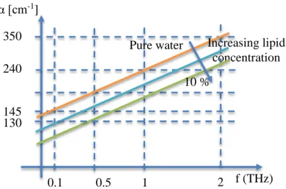
Figure 2 and Figure 3 give a more comprehensive notion about the absorption coefficient in the form of simplified sketches. These figures show only trends and omit the various absorption peaks.
Figure 2 Sketch of the absorption coefficient of air at 1.5 THz
Figure 3 Sketch of the simplified absorption spectrum of water and water-lipid solutions
Of course, the diffraction can also seriously affect the total attenuation, but it has smaller significance on the millimeter scale traveling paths. Additionally, diffraction depends much on the actual structure of the specimen.
Here, I give the needed SNR and detectability to meet the specification with the actual setup at the COSPL. Because of the required minimum water content detectability of 1 %, there is demand for at least 1:100 signal-to-noise ratio that is 40 dB SNR. 1 mm depth means 2 mm travel length (the incident plus the reflected path). For this, the irradiance can be calculated in the following way in a homogeneous medium: I = Iincident∙ e−200∙0.2≈ Iincident∙ 4.24 ∙
6 12.5 25 52
0.8
0.01 α [m-1]
Humidity [%]
0.1 0.5 1 2 f (THz)
145 130 240 350 α [cm-1]
Increasing lipid concentration 10 %
Pure water
- 19 -
10−18 [mW2] (at 𝛼 = 200 cm−1) and for 0.5 mm depth it is I ≈ Iincident∙ 2 ∙ 10−9 [mW2] (at 𝛼 = 200 cm−1).
If I approximate the obtainable SNR (not given in dB) in the following way with the noise floor that is the limit of sensitivity:
𝑆𝑁𝑅 ≈ I∙A
Pnoise floor, then (20)
Pnoise floor≈SNRI∙A ≈Psource∙4.24∙10100 −18= 4.24 ∙ 10−20∙ Psource [W], (21) where “I” is the irradiance and “A” stands for the area of the detector. (For simplicity, I assume perfect focusing to the detector, that is Iincident∙ A = Psource). (21) shows how strong illumination would be needed to achieve these goals with a noise floor in the pW range, what we can get from the noise equivalent power (NEP):
NEPsystem≈Pnoise floor
√B [√HzW ], (22)
where “B” is the bandwidth of the system. It is obvious that this implies infeasible system NEP values even at good frequency filtering regarding the available source power of ~100 µW. Such depth is achievable only with high power sources, heterodyne detection and efficient frequency filtering.
However, the 1 mm depth can be achievable in other tissues with lower absorption coefficient and sensing is still possible at about 0.25 mm depth in biological tissues assuming a minimum NEP of 20 pW
√Hz , 10 Hz bandwidth, ensured by the lock-in amplifier and a minmum required SNR of 100:
𝑧 =1
2 1
𝛼ln (Iincident
Imin ) = 1
400ln (Pnoise floorPsource𝐴
A ∙SNR) = 1
400ln ( 100∙10−6
√10∙20∙10−12∙100) ≈ 241 [μm] (23) See more considerations on the depth of sensing in section 3.4.3.
I conclude the main bottleneck of applicability is the limited SNR of the sensor. Sensitivity has to be improved in order to increase the depth of examination and the acquisition speed.
Moreover, fulfilling the specification of lateral resolution may require silicon immersive lenses or super-resolution techniques.
Today THz FPAs are still far from their theoretical NEP values. The performance of the integrated systems within real application scenarios are often far from the reported best achievable NEP values of the devices [7]. Therefore, it is an important task to study the FPA architectures to help designers improve on system noise particularly for heterodyne detection, where the incoming signal mixes with the signal of a much stronger local oscillator (~10 µW) inside the channel improving the sensitivity several orders of magnitude.
- 20 -
However, with high power sources (W-mW range) imaging at discrete frequencies is already possible in the 0.08-0.2 THz frequency range (see the IMPATT diode powered simple camera systems of TeraSense). The versatility of these low frequency setups imply the future power of imaging in the 0.2-1.5 THz range and motivates the work of the terahertz research group at the COSPL.
Water content measurements can be seen in Section 4.1.1, but Section 4 contains other related experiments as well.
2.2 The goals of my research work - problems to solve
The focus of my work was to study the compressed sensing based THz detectors and their forms of application. This served the ultimate goal of promoting the application of our FET based detectors in the field of THz diagnostics. This emerging research direction raises many basic problems. I list here a few big areas out of which I touched several ones during my work:
Determine the specification of the sensor array
Acquisition speed
Weak signals, low SNR, high noise, small response, low penetration depth
Low resolution (spatial), low NA optics
Small pixel number
Low quality images, low sensitivity, low contrast
Scanning problem (time, accuracy)
Low specificity at sub THz frequencies
2.3 Setup 2.3.1 Source
An yttrium iron garnet (YIG) base oscillator – tunable from 9.5 GHz to 14 GHz – powers the source of the quasi-optical setup that is a semiconductor based amplifier-multiplier chain (AMC). The AMC multiplies the base frequency with a factor of nine providing approximately 14 dBm (~0.25 W) typical output power in the frequency range of 82.5-125 GHz. The output of the AMC is a waveguide and a horn antenna couples the power to the air.
However, additional multipliers may connect to the output to cover higher frequency ranges with decreasing efficiency. Table 2 summarizes the technical data of the different configurations. These are the typical technical parameters of the setup from the datasheets; the measured output power at 460 GHz was 102 µW.
- 21 - Table 2 The characteristics of source configurations
In Figure 4 one can see the output characteristics of the WR2.2 multiplier head. Due to the waveguide-based structure, the spectrum has high variance with many narrow peaks.
The theoretical accuracy of the frequency tuning is on the order of 7 MHz, however any noise of the system deteriorates it. Aside from this, the YIG seems to have relatively high offset error that decreases the absolute precision of the source. Hence, by recording spectral features one has to sweep at higher frequency resolution than the targeted one and average several correlated spectra. This way one can create data appropriate for comparison.
Figure 4 Power spectrum of the utilized terahertz source
The coherence length is around 0.5 m that means great freedom in holographic recordings considering the object and reference path difference, but rises severe technical problems by making the system very sensitive to any physical effects due to self-interference. This means that sub-millimeter (< 100 µm) changes of the optical path can cause over 50% changes in the recorded intensity. This issue makes in-vivo measurements a hard task, where the precise positioning of the body parts for at least tens of seconds is challenging. However, we had problems with in-vitro measurements as well, when solutions of different temperature were investigated: the thermal expansion of the plastic sample holder caused significant discrepancies. Diffusor plates could partially circumvent the problem of high coherence at the cost of decreasing the source intensity.
Head Mult.
factor Configuration Typical
power Frequency range
WR9.0 9 WR9.0AMC + 14 dBm 82.5-125 GHz
WR4.3 18 WR9.0AMC + WR4.3X2 + 3 dBm 170-250 GHz
WR2.8 27 WR9.0AMC + WR2.8X3 -1 dBm 250-375 GHz
WR2.2 36 WR9.0AMC + WR4.3X2 + WR2.2X2 -10 dBm 340-500 GHz WR1.5 54 WR9.0AMC + WR4.3X2 + WR1.5X3 -21 dBm 550-750 GHz
- 22 -
2.3.2 Quasi optical setups
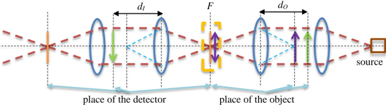
Quasi-optical setups may consists of parabolic mirrors, plastic lenses and beam splitters. Figure 5 presents the schematics of the imaging setups for CS measurements.
Figure 5 A transmissive and a reflective setup is depicted on the left and right side, respectively; the main components are: a) Terahertz continuous wave (CW) source: amplifier-multiplier chain (AMC) and yttrium iron garnet (YIG) oscillator, b) off-axis parabolic mirrors, c) target object d) detector chip e) 3 axis moving stage
The calculation of the sensor and image position is straightforward. For the real image, I used the mirror equation:
1 𝑓= 1
𝑑𝐼+ 1
𝑑𝑂 , (24)
where dI and dO means the distance of the object and that of the image, respectively. Figure 6 gives an overview about the basic configurations and helps to compare them.
Figure 6 The basic image projection methods: a) real image with magnification ratio, 𝑀 = −𝑑𝐼/𝑑𝑂
(green), b) confocal scanning (orange), c) Fourier imaging; the image is also right in the focal plane (purple); lenses are interchangeable with parabolic mirrors; the distances are not proportional
In the case a), the distances are not proportional in the figure, of course, when 𝑓 < 𝑑𝑂 < 2𝑓, then 2𝑓 < 𝑑I.
To measure the resolution of the system in confocal scanning configuration and all pixel activated, I fixed the actual chip on a high precision, 3 axes moving stage. The parabolic mirrors
d)
AMC
YIG freq. mod.
a)
c) b) AMC
YIG freq. mod.
d) a)
c) b)
e)
e) e)
dO
dI F
source
place of the detector place of the object
- 23 -
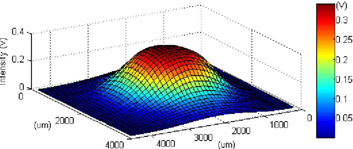
collimated and focused the source beam onto the detector array. The Gaussian like spatial intensity distribution was registered with 100µm precision and presented in Figure 7.
Figure 7 Raw measurement data of the focused Gaussian beam of the terahertz source
2.3.3 Antenna coupled FET detectors
2.3.3.1 Principle of detection
Here, I summarize the principle of FET based sensing and highlight some problems of such detector arrays. These gave additional motivation to make complementary architectural investigations.
Figure 8 The scheme of a Si MOS based terahertz sensor element
In the followings I mean on ‘terahertz sensing’ power intensity measurements in the 125-750 GHz frequency range. Figure 8 shows the scheme of a single detector element, where detection is realized in the channel of an nMOS transistor. The high frequency signal of the antenna arrives to the transistor pads. The free electrons behave similarly as a gas or shallow water [23] under the gate, because plasma waves obey linear dispersion laws (𝜔 = 𝑠𝑘), where 𝜔, 𝑠, 𝑘 denotes the frequency, the wave velocity and the wave vector, respectively. The velocity, 𝑠 = (𝑈𝑒𝑚)1 2⁄ , where 𝑒 and 𝑚 is the charge and mass of the electron, in turn, 𝑈 is the gate to channel voltage.
Therefore, the Euler equations describe the excitation of the two-dimensional electron gas (2DEG) by small amplitude AC signal. The channel has a Reynolds number around 60
planar antenna on top metal layer
GND LNA
pseudo-resistors stabilized bias
feed lines SiO2
Si ground plane
air/passivation
detector transistor output
- 24 -
(regarding HEMTs) as a cavity of the “fluid”. Due to the nonlinearities of the plasma and the boundary conditions, a DC voltage emerges in the active zone of the channel. This is the
“intrinsical” response of the device that is measured through the terminals, presenting a given load to the detector. The loading (or change in the boundary conditions) alters the intrinsical response. In the same time, the transistor works as a common gate amplifier according to the biasing conditions. Therefore, the measured, in-circuit response of the detector depends on the connectings of the antennas, the load and the biasing (among other factors) on a complex way [6].
Noise is another issue that changes on a different way, therefore minimum NEP and maximum response do not coincide.
2.3.3.2 Antenna design
The chief designer, Péter Földesy considered three main types of antenna arrangement for realization:
I. Aperture coupled variants:
a) Chip on board (signal comes from the back through the substrate) b) Chip with covering (signal comes from the top)
c) Chip with suspended covering (optionally with Fresnel aperture) II. Planar antenna laying directly in the top metal layer of the chip
a) Patch antenna
1. Patch with striped, grid structure (to reduce capacitive losses) b) Fresnel aperture antenna
III. Flip –chip –like arrangement with isolating layer – its feasibility is questionable, however this way the distance of the patch and the chip surface could be tuned accurately with the thickness of the isolating layer.
These findings were shown to microwave communication specialists (Gergely Károlyi and Csaba Füzy) for performance comparison estimation. In the followings, I depict the schematics of the different antenna types to reveal the main difficulties of integration (See Fig. 9-13 for details; these are modified, extended versions of figures from [24].). I mention only the two most important problems: which antenna structure can be the most efficient and how to realize the feedline to minimize losses i.e. how to match the antenna to the detector. In the case of aperture coupled realizations the electromagnetic field couples through an aperture – practically a slot in a metal layer – to a planar feedline. This line is a simple metal wire of about 15 µm width with a closing stub at its ends. This stub is an overhang of the wire starting from the geometrical center of the aperture that takes place a few layers above the feedline what lays generally on the first metal layer.
- 25 -
With this, the closing of the feedline can be tuned easily and accurately. Matching of the patch to the detector is only the question of proper distances between the feedline, the aperture, and the patch antenna. However, the distance of the aperture to the feedline can be set only in discrete steps of the metal layers within a very small range relative to the wavelength. The fixing of the patch is another problem. It needs a solid supporting surface that can be metalized. The space holder can be this carrier material itself or some auxiliary support structure (suspended covering). Here, the distance can be set more freely, but the fixing, accurate manufacturing and positioning of the patches is a hard and costly post-processing task. These facts make the variations in group I. and III. disadvantageous from feasibility point of view.
The direct planar antennas are easier to manufacture, however one have to be more cautious during design. For acceptable matching, one has to estimate the input impedance of the detector transistor at frequencies that are above the cut off frequency of the technology and not covered by the conventional channel models.
To steer clear of this problem, that could be solved precisely only with iterative design- manufacture-measure steps, we used the design strategy suggested by Csaba Füzy. According to this, we took the MOS transistor with near threshold gate bias as it was an open circuit from the GS and GD points, where G, S, D are the gate, source, drain contact points, respectively.
Each of us simulated the antenna structures with its feedline and the transistor contacts. The antenna design and characterization was not carried out with the conventional antenna design methods. In that scheme a proper port configuration, often frequency domain simulation and S- parameters calculation takes place. Then the S-parameters are used as the key figure of merit.
In the investigated system, however, the design was driven by the maximal field strength between the transistor contacts.
For this reason, the via stacks that constitute the feedline were not pure vertical columns, but they formed a V-shape approaching gradually the two contact point of the transistor from the opposite sites.
Details with schematics about the antenna connecting can be seen later in chapter 2.4.1.2.
- 26 -
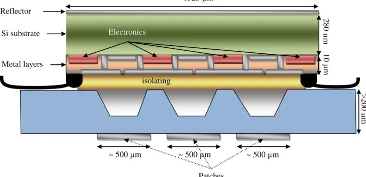
Figure 9 The schema of version I. a) chip on board with reflector.
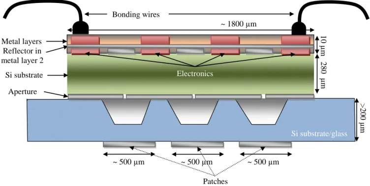
Figure 10 The schema of version I. b) chip with aperture coupled antennas and a covering with patch antennas and optional etched cavities for reducing dielectric losses.
>200 µm
Si substrate/glass
10 µm280 µm
~ 500 µm
~ 500 µm
~ 500 µm Reflector in
metal layer 2 Si substrate Metal layers
~ 1800 µm
Aperture
Patches Electronics
(wiring on metal layers and poly silicon gates) Bonding wires
Patch
~ 500 µm
~ 500 µm
~ 500 µm
Reflector
Electronics
10 µm280 µm
Si substrate
Ground plane with aperture ~ 1800 µm
>200 µm
Metal layers
- 27 -
Figure 11 The schema of version I. c) chip with suspended covering. It can be combined with aperture coupled antennas or simple planar structures.
Figure 12 The schema of version II. b) The schematics of a more sophisticated aperture coupled antenna with polarization insensitive Fresnel aperture (without ordinary patch). In the case of version II. a), there is a simple or striped patch on the top and feed lines are formed from via stacks (see later in details).
Si substrate/glass
Electronics
10 µm 280 µm Ground plane with aperture
>300 µm
Casing Patches
Si substrate
Electronics
10 µm280 µm
Si substrate Metal layers
~ 1525 µm
Hole Metal
layer
Reflector Bonding wires
Metal layer
- 28 -
Figure 13 Version III. Flip-chip-like configuration with an isolating layer.
Figure 14 The envisioned striped, grid-like structure of the patches
I have considered several antenna types within the main categories. For instance, the striped patch antenna (see Figure 14). Patch antennas are broadband, simple to design and easy to manufacture. Their capacitive losses can be reduced if the patch has a grid like structure. If polarization sensitivity is not a problem that is only one receiving direction is used, stripes in only that single direction (no intermediate crossing) or clustered dipole structures can be more advantageous. Yet, it provides the possibility for heterogeneous detection. However, one has to keep in mind the manufacturing antenna rules (this notion is not related to the antenna design) and metallization restrictions during the design.
I have simulated special variants of quad antennas as well as possible compact and high gain solutions. These, antennas were generated by scripts and were easy to modify and optimize them on automated ways.
Si substrate/glass
Patches Electronics
10 µm280 µm
~ 500 µm
~ 500 µm
~ 500 µm Reflector
Si substrate
Metal layers
~ 1525 µm
isolating
>200 µm
l/8 λ or l/10 λ
3-15µm
- 29 - 2.3.3.3 Manufactured chips - premises
The first antenna coupled detector – made at the Intstitute for Computer Science and Constrol of the Hungarian Academy of Sciences (ICSC – HAS) by Földesy [12] – was a proof-of-concept chip manufactured at 180 nm feature size technology with photoconductive antennas on it.
Several detector-antenna connectings and antenna types were tested, but the simplest arrangements provided the highest responsivity; these were used in the later designs.
A 90 nm SoC like monolithic detector array meant the second step, where both single-band and broadband antennas showed up with linear and circular polarization sensitivity. These designs paved the way for a compressed sensing based detector array. Péter Földesy proposed the idea that complex sampling capable THz detectors can be formed from serially connected arrays with individually controllable gate biases. I could also participate in the process and performed the sizing of the antennas according to the methodology determined by our RF experts. I used this chip as a starting point for my investigations and to validate the results with measurements.
2.3.1 A/D conversion
The A/D conversion must be an integrated part of a compact imager; however, experimental use and the need for easier prototyping may waive this requirement. Despite the COSPL had such an SoC-like design, in the experiments we used a commercial external data acquisition card (NI6343) to digitalize the output of the integrated LNA.
The absolute accuracy is usually much lower than that of the pure random noise would allow:
AbsoluteAccuracy = Reading (GainError) + Range (OffsetError) + NoiseUncertainty.
This NI DAQ card had an absolute accuracy of 2190 µV, 1130 µV and 240 µV in the (-10 V, 10 V), (-5 V, 5 V) and (-1 V, 1 V) operating range, respectively – concerning only the applicable opportunities. The belonging RMS random noise (𝜎) was 270 µV, 135 µV and 28 µV, respectively that resulted in a noise uncertainty of 5.7 µV, 2.86 µV and 0.59 µV with 3𝜎 coverage and 20000 samples. In the first two case, the given 16 bit precision (301 µV and 150 µV) is above the limit of the absolute accuracy, however, for the highest absolute precision (30 µV) at least 640 kSamples would be needed at maximal, 1 V readings. After all, the used lock- in amplification relied only on the relative accuracy of the A/D. In a typical operation configuration – (-5 V, 5 V) range, 2,5 V peak reading, relative measurements, 20 kSample – the
‘gain error noise’ is 163 µV whereas the random noise is 2.86 µV, therefore the system approaches the precision of the quantization (153 µV).
It follows that the A/D conversion meant no bottleneck in the read-out circuit.
2.4 180 nm Serially connected sensor array
The subject of my work links closely to the manufactured detector; therefore, I describe it in details in this separate section [2].
- 30 -
To create images from the aggregated response we perform multiple complex measurements and optimization based reconstruction. In order to reduce also the acquisition time we can utilize the sampling scheme of compressed sensing. For this, one has to control the contribution of the individual detector elements to realize the complex measurements (represented by the matrix, Φ).
The solution of the COSPL at the ICSC – HAS allows complex sampling by exploiting the specialties of FET plasma wave detectors in the THz region. The two domains have significant implementation differences as orders of magnitude lower source power and plasma wave detection challenge actual analogue VLSI techniques.
The proposed solution reduces the noise of the created images in the following ways:
A common practice to increase the signal level of voltage-based detectors is to bind multiple ones in series [13]. Elkhatib et al proved in [14] and [15] that the response of FET plasma wave detectors also adds up and scales linearly with the number of involved devices. (The thermal noise also increases, but only with the square root of the number of detectors.)
Of course, the per pixel SNR remains the same, but this increase of the sensor SNR means higher, shifted signal level that is advantageous by the amplifier implementation.
Compressed sensing reduces the needed sample count and decreases noise directly as well as the non-linear reconstruction can suppress Gaussian noise to certain extent [16].
As the pixel cluster is serially connected, only one low noise amplifier (LNA) contributes to the output noise per cluster.
2.4.1.1 The working principle
In the case of FET based terahertz sensing, it is possible electronically controlling the photoresponse of each serially connected sensor elements. Figure 15 shows the typical response of a detector against UGS that we measured on the proof-of-concept chip of the COSPL in open circuit mode. This indicates that we can significantly reduce the photoresponse and resistance contribution (i.e. thermal noise) of a given detector to the output by fully opening the detector transistor (“OFF” state). The created detectors are 1.8V standard transistors on a 180 nm CMOS technology. Worth to note, that the optimal gate bias voltage for the “ON state” depends on the number of active pixels. Moreover, they not necessary coincide with the maximum responsivity gate bias [15]. However, even a single, general bias voltage can provide acceptable performance (see measurements in section 4). This allows utilizing only simple, binary pattern generator circuitry with only two constant reference voltages (e.g. 0.35V and 1.8V). The exponentially increasing current induced flicker noise becomes dominant in subthreshold operation region, thus NEP minimum turns up at higher gate voltage regions.
- 31 -
Figure 15 A measured, typical response of the detector array at different gate-source voltages
The frequency characteristics of the array is showed in Figure 16. This measurement was carried out with all pixels activated by uniform gate bias.
Figure 16 Average frequency characteristics of the detector array in the 330-480 GHz range
The originally targeted frequency was 470GHz to accommodate the specific power spectrum of the given AMC source. Because of the computational burden of precision, the simulations were done in two rounds: first with simplified structures and afterwards with the precise model of the chip including the dielectric layers, passivation and exact copy of the 3D structure exerted from the output of the layout program.
Comparing the simulation results of isolated, standalone versions and densely populated arrays of several pixels showed that frequency shifts upwards if more detectors are arranged near to each other. Figure 17 Part B and Part C is an example that shows that besides the reduction of gain a frequency shift with a factor of about 1.0187 occurs.
Thus, optimizations can be done on simplified models of isolated antennas by decreasing the target frequency to 460GHz. In the second round, the corresponding precise, isolated structures have a resonance frequency of 450 GHz (see an example in Fig. 10 Part A). Hence, the expected frequency peak for the array was about 458 GHz. On the chance that several other, non- simulated effect can increase the resonance frequency, we have kept this configuration.
- 32 -
Figure 17 Resonance frequencies of different simulated structures
2.4.1.2 Details of the prototype detector array
Figure 18 The scheme of a MOS based terahertz sensor element (figure repeated from section 2.3.3.1) The detector array performs power intensity measurements at a single frequency of 460 GHz.
Figure 18 shows the scheme of a single detector element, where detection is realized on an nMOS transistor by self-mixing. Considering the 125-750 GHz source frequency range and the Si MOSFET detector of 180 × 300 nm2 size the non-resonant, long channel approximation applies [8]. Manufacturing came off at standard CMOS 180 nm technology sparing any extra post-processing. The antenna arms connect directly to the gate and source terminals of the detector transistor with the 𝛾-shaped vertical structure built from via arrays and metal layers;
see Figure 20 Part C. Thin, high inductivity wire connections ensure the proper biasing of the FET. Their placing is a crucial design step, especially at not nodal regions, because these contacts can fundamentally change the resonance of the antenna.
a)
b) c)
planar antenna on top metal layer
GND LNA
pseudo resistors
stabilized bias output detector
transistor
feed lines SiO2
air/passivation
Si ground plane


![Figure 19 Schematics of the low noise amplifier a) shows the band pass amplifier filter and b) shows the telescopic OPA (This figure is from Földesy [6].)](https://thumb-eu.123doks.com/thumbv2/9dokorg/1305547.105040/33.892.234.717.493.750/figure-schematics-amplifier-amplifier-filter-telescopic-figure-földesy.webp)

