Low Resolution Infrared Proximity Array Based 3D Object and Force Reconstruction, and
Modular Oscillatory Arrays
Akos Tar ´
Faculty of Information Technology P´ azm´ any P´ eter Catholic University
Scientific adviser:
Gy¨ orgy Cserey, Ph.D.
A thesis submitted for the degree of Doctor of Philosophy (Ph.D)
2011
I would like to dedicate this thesis to my loving family ...
Acknowledgements
First of all, I would like to thank my supervisor Gy¨orgy Cserey for in- troducing me to scientific work and for his constant support in bringing our ideas into reality and believing in my research activity.
I am thankful for the P´azm´any P´eter Catholic University Faculty of Information Technology and the Multidisciplinary Doctoral School for providing tools and a caring environment for my work, especially per- sonally for Judit Ny´ekyn´e-Gaizler, Tam´as Roska and P´eter Szolgay.
I would like to thank to my closest colleague J´ozsef Veres for the long- lasting joint work during these years. The cooperation of my col- leagues at the Robotics Laboratory Norbert S´ark´any, Mikl´os Koller, Ad´´ am R´ak, Norbert H´oz, Bal´azs J´akli, Gergely So´os, Gergely Feldhof- fer, Alp´ar S´andor, Ferenc Lombai and Gandhi Gaurav is greatly ac- knowledged. The work with them greatly contributed to my scientific results.
I would like to thank also my fellow PhD students and friends for their help, especially to D´avid Tisza, P´eter Vizi, J´anos Rudan, Zolt´an Tuza, D´aniel Szolgay, Andr´as Kiss, G´abor Tornai, L´aszl´o F¨uredi, Zolt´an K´ar´asz, Andrea Kov´acs, Vilmos Szab´o, K´alm´an Tornai, Bal´azs Varga, Tam´as Pilissy, R´obert Tibold, ´Ad´am Balogh and Endre L´aszl´o.
Thanks especially for the discussions and ideas to G´abor Szederk´enyi, Andr´as Ol´ah, Attila Kis, G´abor V´as´arhelyi, Krist´of Iv´an, ´Eva Bank´o, B´ela Weiss, Krist´of Karacs and Attila Tihanyi.
Special credits are also for the endless patience and helpfulness to Mrs Vida, L´ıvia Adorj´an, Mrs Haraszti, Mrs K¨ormendy, Mrs Tihanyi and Mrs Mikesy and the rest of administrative and financial personnel.
Special thanks go to Sarolta Tar, Mikl´os Gy¨ongy and Zs´ofia Cserey who helped a lot in the English revision of the text.
The Operational Program for Economic Competitiveness (GVOP KMA), The office of Naval Research (ONR) and the Hiteles Ember Foundation for their support are greatfully acknowledged.
For the outstanding support of bringing the CAD models into real- ity with 3D printing technology I would like to thank to VARINEX Informatikai Zrt.
The loving support of all my family and my wife Bernadett helped me through the hardest moments of this period.
List of Figures
2.1 A photograph of the sensor array . . . 8 2.2 Schematic diagram of the infrared LED control . . . 9 2.3 Schematic diagram of the photodiode readout circuit . . . 10 2.4 The two experimental setup groups where the sensor array was tested 12 2.5 Distance measurement method, theory of operation . . . 15 2.6 Difference between the real θ and estimated θ0 values at different
number of iterations . . . 16 2.7 Measurement and simulation result of the sensor array of an object
placed 20 cm above, with and without angle of incidence correction 19 2.8 Scanning result of different kind of objects (cube, U-shape and H-
shape) . . . 20 2.9 Test case where the previous version of the sensor array was attached
on a bipedal robot feet in order to detect obstacles . . . 22 2.10 Scan result of different landmarks. On the top are the pictures of
the used landmarks and on the bottom the images created with the sensor array attached on a mobile robot. . . 23 2.11 Experimental result of a door-step detailed detection with a Power-
Bot type mobile robot, where the sensor was mounted on the front bumper of the robot and was directed to the ground. . . 25 2.12 Localization experiment with the PowerBot type mobile robot . . . 26 3.1 Schematic drawing of the tactile sensor . . . 33 3.2 The data acquisition board and a connected tactile sensor prototype. 34 3.3 Shematic drawing of the reflected lighs . . . 35 3.4 Deformation of the semicircle . . . 37 3.5 Experimental setup to measure the tactile sensor pressure profile
along an axis . . . 39 3.6 Setups for measuring noise, impact and stroke . . . 40
3.7 Static load response of the tactile sensor . . . 42
3.8 Maximal load measurement . . . 43
3.9 Sensor output characteristic . . . 44
3.10 Error between the real and calculated force incidence angle . . . 45
3.11 Calibrated tactile sensor output . . . 46
3.12 Force measurement form different directions . . . 46
3.13 Noise, hammer impact, and brush stroke measurement . . . 47
3.14 Pulse shape measurement . . . 48
3.15 Measurement of the realaxation characteristic at different load levels. 49 3.16 Relaxation characterictic after the load was removed. At 0.25 s all signal value dropped at least 86% and after a certain time returned to zero. . . 49
3.17 The three layered sensor structure. . . 50
3.18 The moulding process of the elastic cover . . . 53
4.1 Current vs. voltage characteristics of the Chua’s diode . . . 57
4.2 Chua’s Circuit Schematic . . . 58
4.3 Snapshot of the Chua kit . . . 60
4.4 Snapshot of the second version of the Chua kit . . . 61
4.5 Chua kit with the extension borad . . . 62
4.6 General architecture of programmable logic layer . . . 63
4.7 Coupling grid . . . 64
4.8 The topologies and the weights, which were used in the experiments 65 4.9 Two connected Chua’s circuit at 0 Ω and at 10 K Ω . . . 66
4.10 The Chua’s circuits moves from de-synchronization to synchronization 66 4.11 SPICE simulation of two connected Chua’s circuits at 10 KΩ . . . . 67
4.12 SPICE simulation of two connected Chua’s circuits at 1 KΩ . . . . 67
4.13 SPICE simulation of two connected Chua’s circuits at 6.5 KΩ . . . 68
4.14 Simulation of the phase transition . . . 68
4.15 Ten Chua’s Circuits were connected in 3D in a cross like topology . 70 4.16 Connecting 3x3 Chua’s circuits . . . 71
4.17 A picture of the experimental setup where eight Chua’s circuits were connected . . . 72
Summary of abbreviations
Abbreviation Concept
SLAM Simultaneous Localization And Mapping P SD Position Sensing Device
U S Ultrasound Sensor
T oF Time of Flight
LED Light Emitting Diode
DAC Digital to Analog Converter ADC Analog to Digital Converter SP I Serial Peripheral Interface
P C Personal Computer
LIP A Large Infrared Proximity Array M EM S Microelectromechanical Systems F SR Force Sensing Resistor
DOF Degree Of Freedom
P CB Printed Circuit Board
LU T Look Up Table
M SB Most Significant Bit LSB Least Significant Bit
CAD Computer Aided Design
EEG Electroencephalography CN N Cellular Neural Network M U X Multiplexer
SP ICE Simulation Program with Integrated Circuit Emphasis
Contents
Acknowledgement i
List of Figures v
Summary of abbreviations viii
Contents ix
1 Introduction 1
1.1 Research Goals . . . 3
2 Infrared Sensor Array 5 2.1 Introduction . . . 5
2.2 General description of the sensor array . . . 8
2.3 Experimental setup . . . 11
2.3.1 Object scanning experiment . . . 11
2.3.2 Mobile robot experiment . . . 13
2.4 Signal post processing . . . 14
2.4.1 Sensor model . . . 14
2.4.2 Edge reconstruction and object outline detection . . . 16
2.5 Experimental results . . . 18
2.5.1 Measuring the angle of incidence . . . 18
2.5.2 Object scanning experiments . . . 18
2.5.2.1 Edge reconstruction and object outline detection . 18 2.5.2.2 Surface trace . . . 20
2.5.2.3 Image registration . . . 21
2.5.3 Mobile robot experiments . . . 22
2.5.3.1 Landmark detection . . . 22
2.5.3.2 Door-step detection . . . 24
2.5.3.3 Map building (SLAM) . . . 24
2.6 Conclusion . . . 27
3 Complaint 3D Tactile Sensor 29 3.1 Introduction . . . 29
3.2 Design concepts . . . 31
3.3 Sensor description . . . 32
3.3.1 Theory of operation . . . 35
3.4 Experimental setup . . . 38
3.4.1 Static calibration of the sensor . . . 38
3.4.2 Characterization of the sensor . . . 38
3.4.3 Sensor capabilities . . . 40
3.5 Signal post processing . . . 41
3.6 Experimental results . . . 42
3.6.1 Static calibration of the sensor . . . 42
3.6.2 Characterization of the sensor . . . 43
3.6.3 Measuring the force incidence angle . . . 43
3.6.4 Calibrated sensor output . . . 44
3.7 Sensor capabilities . . . 45
3.7.1 Force directions . . . 45
3.7.2 Noise performance . . . 45
3.7.3 Hammer impact . . . 46
3.7.4 Brush stroke . . . 47
3.7.5 Pulse measurement . . . 47
3.7.6 Relaxation time . . . 48
3.8 Layered structure of the elastic cover . . . 50
3.9 Sensor prototyping . . . 52
3.10 Conclusion . . . 54
4 Studying Synchronization Phenomenon in Oscillatory and Chaotic Networks 55 4.1 Introduction . . . 55
4.2 Chua’s circuit . . . 56
4.3 Chua’s circuit kit . . . 59
4.4 Chua’s circuit grid - general architecture . . . 59
4.5 Architecture implementation . . . 61
4.5.1 Interconnecting interface . . . 61
4.5.2 Programmable logic . . . 62
4.5.3 Coupling grid . . . 63
4.6 Experimental results . . . 63
4.6.1 Case 1. one dimensional coupled Chua’s circuits . . . 65
4.6.2 Case 2. two dimensional coupled Chua’s circuits . . . 68
4.6.3 Case 3. three dimensional coupled Chua’s circuits . . . 69
4.7 Discussion . . . 73
4.8 Conclusion . . . 74
5 Summary 75 5.1 Main findings and results . . . 75
5.2 New scientific results . . . 75
5.3 Application of the results . . . 76
Bibliography 81
Chapter 1 Introduction
Emergence is a prevalent phenomenon in nature, when the cooperation in a simple ruled system results the arise of a new feature or a new behavior (e.g.: cells form organs). It is also interesting from an engineer point of view, where the interaction of each element in a system could improve the overall performance (e.g: interpo- lation) or new features can arise (e.g: robot cooperation). Therefore during my research I aimed to use topologies where the interaction of the cells enhanced the overall system performance.
The two main research fields:
• Novel sensor technology to improve the environment recognition in robotics
• Synchronization in coupled oscillatory networks
The presence of robotics made the first breakthrough in the industry. Their accuracy, workload capacity, reliability, have allowed high-quality and low cost mass production. Since then, of course, big variety of size, shape and structure robots has been developed. Due to the technological developments and research robots are getting very common. There are plenty of solutions, which have been trying to ease our ordinary life. Their appearance is tending to be more human like as in a man-made word, a humanoid robot can adopt to the human made tools and devices much more easily. For a humanoid robot, it is essential to walk.
This is a very interesting and intensively researched field, but we are still far from the robust and stable walking. Although much progress has been made, there are already statically stable walking robots [8, 9, 10] and there are some good examples of dynamic walking [11,12, 13].
Despite all this for the widespread use of robots we still have to wait. In a well modeled environment even without sensorial feedback, they can already execute a number of tasks [14], but they cannot adopt to a dynamic environment. The problem is that robots must sense their environment, they must be connected with the surroundings.
Humans during walking preidentify the obstacles ahead, their size, position, ori- entation with the aid of vision (contactless sensing), and we can immediately mod- ify our walking in order to avoid the obstacles with the lowest energy. Researchers tried to use vision systems to do the same with humanoid robots [15, 16, 17] and also equip with basic reflexes using contact based sensing [18]. However due to the high computation power (object classification, image registration, 3D vision) it is hard to make real time control. Furthermore, today robots cannot divide their vi- sual attention between navigation or detecting interactions from the environment, thus usually separate camera systems are used to each task [8].
This is why it is essential to use such a sensor (sensor systems) that produces reliable and substantial information at low computation power. An other solution cold be to use many sensors as a distributed system. Use separate sensor or sensors (even in a reflex level) for example for obstacle detection that can provoke the visual attention for identification and to make the necessary avoidance manoeuvres.
During our MSc studies with my collage J´ozsef Veres we build a bipedal robot [3].
Our experimental results also demonstrated that in order to achieve stable and robust walking it is crucial to connect the sensed environment into the control (e.g: how the robot is standing respect to the ground).
Hence during my research I tried to create hardware implemented contact base and contactless sensors (than can be used in any field of robotics) wherewith the perception of the environment can be improved at low computation power.
The other interesting research field is the coupled oscillatory arrays whose syn- chronization is a prevalent phenomenon in nature [19]. Within this the chaotic systems are already well-known for strange patterns in their phase space, which has always attracted the research community [20, 21]. Even more stranger pat- terns can be observed in case of two or more chaotic system connected in different topologies [22]. Researchers already showed chaotic behavior in the brain using EEG [23, 24]. Experimental results demonstrated formation of chaotic oscillation in some part of the brain before an epileptic shock, where the propagation of the spiking can be blocked with in-depth brain stimulation [25]. The same phenomena
was also detected in case of arrhythmia [26]. To understand this kind of patterns and phenomenons it is essential in order to create new cure or medical treatments.
However, until now most of the studies are based on only software simulations.
Therefor during my research I investigated an implementation where oscillators (even chaotic oscillators) can be connected with variable weights and topology.
With this tool, the software simulations could be validated or with using dif- ferent topology and coupling weights new phenomenons may be observed or even the real time behavior of simple (chaotic) oscillatory systems could be modeled.
1.1 Research Goals
The aim of my research was to create sensors (sensor arrays) to improve the today robots’ capabilities to sense the environment. It was divided into two parts contact- less and a contact based sensing. Contactless sensing is used to detect obstacles, distances, outlines, occupied areas during the robot motion remotely. Contact based information is more connected with the sensed object physical properties where the stiffness, weight (forces), or even force distribution for balancing must be detected.
Another goal was to create such a hardware implemented flexible architecture, where interconnected oscillators behavior can be examined in real time in case of different topology using several types of interconnection elements.
Chapter 2
Infrared Sensor Array
2.1 Introduction
An essential function of mobile robots is to navigate safely around their environ- ment. This function is necessary regardless of their main objective, be it pure obstacle avoidance, object picking and placing, or in a more complex case, simul- taneous localization and mapping (SLAM). Since mobile robots are often placed in unknown environments, the use of sensor-based data to achieve object detection, classification and localization is often a challenging problem. The more quickly and precisely the robot can obtain sensorial information about its vicinity, the faster and more reliably it can react. Assuming that contact with unwanted objects should be minimized, all of the above tasks rely on distance measurement sensors.
Robots often need to know how far an object is, what it looks like and what its orientation is. Camera systems are already used for creating 3D images of the environment [27, 28], but mobile robots seldom use the data provided by cameras for low level obstacle avoidance due to high computation power requirements. More often, 2D laser scanners are used with a tilt mechanism to create the 3D scan of the environment [29]. Despite their accuracy, their size and price present a serious drawback. Traditional distance measurement sensors such as ultrasonic and infrared Position Sensing Devices could also be used for creating 3D images of an object [30],[31].
Ultrasonic (US) and offset-based infrared Position Sensing Devices (PSD) are widely used in order to determine the distance of an object. US sensors measure the time of flight (ToF) of the ultrasound signal emitted and reflected to the receiver.
A typical single data acquisition time for an object placed 50 cm away from the
sensor is 3 ms. The main disadvantage of this kind of sensor is the poor angular resolution. The detected object could be anywhere along the perimeter of the US beam due to the wide (typically 35◦) angular sensitivity of the receiver. Because of their relatively large size (of the order of d = 15 mm), dense arrays cannot be constructed.
Offset-based infrared technology uses much narrower beams, both in the case of measuring amplitude response and the offset of the reflected light. The most com- mon offset-type infrared sensors are the Sharp GP series. They are very compact (with a surface area of 44 mm × 13 mm), and have a low cost (∼10 US dollars).
These analog sensors are available in various measurement ranges, the shortest sensing distance being 4 cm (Model GP2D120, range 4 – 30 cm), and the maxi- mum being 5.5 m (Model GP2Y0A700K, range 1 – 5.5 m). In some applications, even these compact dimensions and measurement ranges are not adequate. To fur- ther complicate matters, the sensor has a maximum readout speed of 26 Hz (38 ms) and the output signal varies nonlinearly with distance. Researchers already proved it to be useful for object detection [32] and for creating surface-traces of various objects [30], and for localization purposes [33,34], but because of the sensor speed, real time operation cannot be achieved in many applications.
In this chapter a new reflective type infrared LED and photodiode based dis- tance measurement array is demonstrated as well as its potential usage for tracing object outlines, surfaces and SLAM. The advantage of using a sensor array in the detection of the angle of the reflected light and in increasing the pixel resolution will also be demonstrated.
Although using the amount of reflected infrared light to measure distance is a well-established method, its current applications are mainly restricted to object avoidance, object detection and docking guidance [35]. In these applications, only one LED-photodiode pair is used. The reconstruction of object outlines or surfaces with many LED-photodiode pairs has not been studied yet. The main reasons for this lack of research are the limitations of such detectors, namely the nonlinear output characteristic and the high dependence of the received light on the reflective properties of the object.
Despite the above limitations, the inherent high spatiotemporal resolution and compact dimensions of infrared LED-photodiode pairs make them an important competitor to other distance measurement methods. In contrast to other previously mentioned methods such as ultrasound, the readout speed can be of the order of MHz, and the analogue nature of the signal guarantees a high spatial resolution,
with the readout circuitry and analog-to-digital conversion being the main limiting factors. Indeed, it has been shown that LED-photodiode pairs are a viable way to measure distances in the submicron [36] as well as decimeter [37] range.
There are some outstanding articles that utilize infrared sensors for distance estimation ([36,38,39,40]) and for localization purposes ([41, 42,43]). The key is if a prior assumptions about the given object distance (based on a US, PSD sensor) or reflective properties of the object is given then the reflective type infrared sensors can be used responsibly, or another good method is to try to find the maximum energy of the reflective light [44]. However, with such knowledge distance cannot be measured accurately since the sensor gives the same result if the sensed object is close or it is white. It should also be noted that in the articles mentioned previously, typically only a few infrared sensors are used on the robots (1 or 2 on each side), each sensor is independent, and the infrared LED control is an on- off type. In [45] infrared sensors are used for creating analogue bumpers for a mobile robot and for detecting whether an object is within range or not. As a precursor to the method applied here, two infrared transceivers were used in [46]
to detect object orientation. Here, a more accurate iterative method will be shown to calculate the object orientation. Pavlov et al. [47] showed how cylindrical object location, trajectory and velocity of motion can be determined with 3 pairs of highly directional infrared LED and photodiodes.
Building on our previous work ´A. Tar et al. [4], a better sensor model and an iterative method is given to calculate the angle of incidence, thus achieving a more precise distance measurements with improved electronics.
2.2 General description of the sensor array
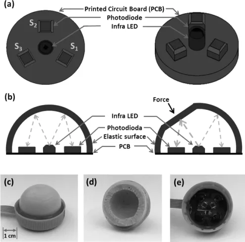
Reflective type infrared sensors that have a coupled optical pair mounted in a re- flective configuration are readily available (e.g. Model TCRT1000, Vishay Ltd, US). These compact sensors only have one separator (between the infrared LED and receiver) which could cause crosstalk in the array. In order to maintain maxi- mal flexibility in the design and in order to be able to equally space the emitters and the detectors in the array, the current work uses individual infrared LEDs and photodiodes.
The infrared sensor array considered in this work consists of 8 infrared LEDs and 8 photodiodes equally spaced in a 120 mm wide row, giving an 8 mm separation distance (see Fig. 2.1). The infrared LEDs (Model TSHF5210, Vishay Ltd, US, 5 mm wide) was chosen to be highly directional with a narrow ±10◦ angle of half intensity. Its peak wavelength is 890 nm, with a typical operating current of 100 mA producing a radiant intensity of 180 mW/sr. By using only short 100 µs pulses, a current of 1 A may be used, which provides an intensity of 1800 mW/sr.
Figure 2.1: A photograph of the sensor array. The infrared LEDs (L) and pho- todiodes (D) are mounted on a regular grid of 8 mm cells. The middle black part acts as a separator between the infrared LEDs and photodiodes. On the top, the number of the measured pixels (measured distance) are indicated and the way they are measured is shown. Data is gathered from photodiodes on either side of each LED, so the first pixel is measured with the first photodiode while the first infrared LED is on, the second pixel is measured with the first photodiode but using the second infrared LED illumination and so on. The array layout and this measurement method will also help to determine the angle of incidence.
Each infrared LED in the row is switched independently with a PMOS tran-
sistor and only one LED state is on at a time. A dynamic current control is also implemented, using another PMOS transistor the gate of which is driven by a 16-bit resolution Digital Analog Converter (DAC). As the DAC output voltage is decreased the transistor drain-source resistance (Rds) also decreases. Hence, the current that flows through the LED can be controlled precisely. The schematic diagram of the LED control is shown in Fig. 2.2.
Figure 2.2: Schematic diagram of the infrared LED control. The infrared LED is switched ON if 0 voltage is applied on the PMOS transistor gate labeled with LED. The second transistor limits the maximal forward current. Its resistance (Rds) is proportional to the voltage applied on its gate with a 16-bit resolution Digital Analog Converter (DAC).
The light received by the photodiode generates a photo-electric current that is converted and amplified with a rail-to-rail amplifier. The output changes from 0 V (no reflection) to 5 V (saturation). In our experimental setup, this creates an effective distance measurement range of 30 cm at 250 mA. The circuit schematic is shown in Fig. 2.3. The anode of the photodiode (Model BPW34, Vishay Ltd, US, 5.4 mm long, 4.3 mm wide) is connected to −5 V. This improves the sensor’s transient behavior. Although the photodiode packaging is different from the in- frared LED, this is because the photodiodes in the 5 mm diameter packaging have a much smaller radiant sensitive area. This version has a 2.65 ×2.65 mm radiant sensitive area with a 0.65 A/W spectral sensitivity at 850 nm.
Each sensor output is directly connected to a 24-bit resolution ADC (Model ADS1258, Texas Instruments, US). The ADC has a built-in 16 channel analog multiplexer and an 8-bit general purpose I/O register. The ADC sampling rate with auto scan (through the 16 channels) is 23.7 kSPS per channel. This module is configured via Serial Peripheral Interface (SPI) and its general purpose I/O port is also accessed in this way. The 8-bit general purpose I/O port is used to
Figure 2.3: Schematic diagram of the photodiode readout circuit. The photo- electric current generated by the reflected amount of light is converted to voltage and amplified with a precise amplifier.
control the infrared LED on/off state in the row. The DAC shares the same SPI port with the ADC that is driven by a microcontroller running on 64 MHz (Model dsPIC30F4013, Microchip, US). It is also responsible for the communication to the PC via a USB port. In the test environment a PC was used to process the sensor data as the aim was to demonstrate the capabilities of the sensor array in general and not limited by the computation power. Nevertheless, efforts had been made to use those methods that can also be implemented on a microcontroller. It should also be noted that the ADC and DAC devices have higher accuracies than were needed in the experiments, so the infrared LED current was quantized to 10 mA steps and only 16-bit sampling was used at the sensor readout.
2.3 Experimental setup
The capabilities of the infrared sensor array were tested in two different setups. In the first setup the movement of the production line or mobile robot (including sen- sor guided wheelchairs) was simulated, where the motion in x, y, z direction could be measured based on sensorial data (e.g odometry) and straight line movements were expected. In the second setup a PowerBot type mobile robot [48] was used.
2.3.1 Object scanning experiment
In this setup (Fig. 2.4/I.) a wooden cube, U-shape and a LEGO H-shape was measured (Fig. 2.4/a,b,c). These objects were chosen as their dimensions are comparable with the sensor array resolution. The sensor array was placed on the z axis of anx, y, ztable that was capable of moving with 10µm precision. The sensor array was moved only in theydirection and no movement was made in thexandz axes. Since an 8×8 sensor array was tried to be modeled, the incrementation step in the y direction was set to 8 mm. The angle of incidence was only approximated in thexdirection based on the measured pixels values in the array. In the scanning procedure 3 different resolutions could be distinguished. The resolution in:
• x - the distance between the infrared LEDs and photodiodes in the array (pixel resolution)
• y - the incrementation step that the table was moved (array resolution)
• z - the used measurement range and the used data converter (in depth- resolution)
The scanning process was as follows:
1. Thex, y, z table was moved to the starting position
2. Measurements were taken with the sensor array, which included offset and ambient light cancellation
3. The table was moved 8 mm in the y direction 4. The measured data was sent to the PC
5. The binary output of the sensors was converted to distance on the PC
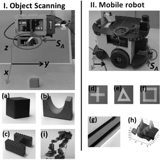
Figure 2.4: Two experimental setup was made. In the first the sensor array was attached on the z axis of an x, y, z table that was capable of moving with a10 µm precision. The sensor array (SA) was moved only in the y direction, and each scanned object (a,b,c) was placed on the xy plane. Simulating a bipedal robot motion (i) an obstacle detection experiment was made with the previous version of the sensor array [4]. In the second setup the sensor array was attached onto the rear bumper of a PowerBot type mobile robot. The robot was driven with a constant speed of 0.2 m/s on a smooth flat surface. The sensor array was at a distance of 65 mm from the ground and looking down to the floor. The sensor array was tested for detecting on-road landmarks for localization purposes (d,e,f), door-step detection (g) and also a potential usage as supplementary sensor for SLAM was tested (h).
An additional experiment (Fig. 2.4/i) with the previous version of the sensor array [4] was made. A case were the LIPA (Large Infrared Proximity Array)was mounted on a bipedal robot feet was tried to be modeled. During the robot motion the feet position of the swing phase leg can be calculated thus the appropriate sensor output at each position can be registered and a higher resolution image can be generated. To validate this theory this sensor array was also mounted on the plotter table in the same configuration but it was also moved in the xdirection.
2.3.2 Mobile robot experiment
The sensor array was attached onto the rear bumper of a PowerBot type mobile robot. The robot was driven with a constant speed of 0.2 m/s on a flat surface.
The sensor array was at a distance of 65 mm from the ground and looking down to the floor (Fig.2.4/II.). As the robot was moving, several measurements were taken with the sensor array: the sensor array was tested for on-road landmark detection for localization purposes (Fig.2.4/d,e,f), door-step detection (Fig.2.4/g) and also a potential usage as a supplementary sensor for SLAM (Fig. 2.4/h).
2.4 Signal post processing
2.4.1 Sensor model
A general description of the sensor model will now be given, including a method to obtain the angle of incidence. As has been mentioned, the current work uses a linear array of 8 LED and photodiode pairs. The central idea of this section is that by combining emitters and receivers across pairs, a resolution greater than the spacing between LED and photodiode pairs can be achieved. The method of building up an image pixel by pixel is now described. Data is gathered from photodiodes on either side of each LED. The value of the first image pixel is generated by measuring with the first photodiode during the first infrared LED emitting, the second pixel is obtained with the first photodiode and the second infrared LED and so on. This method results in 15 pixels in the array as can be seen in Fig. 2.1. The array layout and the described pixel measurement method will also help to determine the angle of incidence. A pioneering work by G. Benet et al. [36] introduced the concept of using the inverse square law to determine the distance of an object instead of the Phong illumination model. In keeping with this law, Eq. (2.1) describes the dependence of the sensor outputy(x, θ), onxand θ, wherex is the distance of the object and θ is the angle of incidence.
y(x, θ) = αi·α0·cosθ
x2 +β (2.1)
where αi is the reflective properties of the sensed object at the viewing area, α0 is constant (accounting for the radiant intensity of the used infrared LED, spectral sensitivity of the photodiode, and the amplification), and β accounts for the level of ambient light and the offset voltage of the amplifier. Because the photodiodes do not have daylight filter attached, a measurement is taken without infrared emission to obtain β due to ambient light and the offset voltage of the amplifier.
The αi parameter is usually obtained by using other distance calibration with another distance measurement method such as US [49] (a distance measurement is made with US and using Eq. 2.1 αi can be calculated).
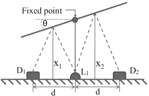
An iterative solution to estimating the angle θ is presented. From Fig. 2.5, it can be seen that
Figure 2.5: This figure shows part of the sensor array, two photodiodes (D1, D2) and between them an infrared LED (L1). The infrared LED illuminates the target surface, which reflects the light to photodiodes with the angle of incidence θ. The distance based on the first sensor reading is x1, and x2 for the second sensor. The d parameter indicates the distance between the infrared LED and the photodiode.
θ = arctan(x2−x1
d ) (2.2)
where x1 and x2 are the perpendicular distances of object points (see Fig. 2.5) and dis the spacing distance between photodiodes and LEDs on the sensor board.
Using estimates θ0,x01,x02 of the true values the following simple iterative steps are taken:
1. Initialize θ0 to 0◦
2. Calculatex01, x02 using (1) 3. Calculateθ0 using (2)
4. Go back to (2) until convergence
The process is deemed to converge when the difference between two consecutive estimates of θbecomes lower than a given threshold, in this case 1◦. Fig. 2.6shows the measurement errors at 0, 1 and 2 iterations for a number of angles in the −45◦ to 45◦ range. It can be seen that at every iteration step, the error decreases by
about 25%. With only two iterations, the maximum error is already less than 0.3◦, meaning only about ±6 µm uncertainty in the measurement when the angle of incidence is around 45◦. This iterative process can be done without requiring new sensorial data so it is implemented very fast, even on a microcontroller. With this method the iteration number can be dynamically varied based on the requested precision or on the current value of the angle of incidence.
Figure 2.6: Difference between the real θ and estimated θ0 values obtained with Eq. 2.2, with different number of iteration used. It can be seen that the error level after the second iteration process is smaller than 0.3◦ at the angle of incidence 45◦. This corresponds to a ±6µm uncertainty in the measurement.
2.4.2 Edge reconstruction and object outline detection
Even though the infrared LEDs are highly directional, some light does get reflected off the sides of the scanned object, causing blurring along the scanning direction.
To counter this effect, a fourth order polynomial fit is made in the scanning direc- tion and normalized into a 0-1 range. The image is then scaled using the normalized polynomial fit. This operation preserves the face of the object while sharpening the edges. It is emphasized that in the case of a 2D sensor array, the need for mechanical scanning – and hence the need to deblur – arises less often.
The outline of the object has to be known in order to have safe navigation or to make interaction. For example, a robotic manipulator has to know the occupied
areas in its working space at a given height for avoidance or for picking or placing objects. As the infrared sensor array supplies single view 3D back projection images of the object by creating a surface cut at a certain threshold, the resulting images will indicate the occupied areas at the height of the cut. To determine this threshold one solution could be to make the cut near to the detected ground.
Alternatively the threshold could be determined according to a specific task: for example, in the case of the robot manipulator, the height of the cut could be the same height where the end effector is, or in the case of a mobile robot it could be the height of the maximum object which the robot can drive through without a problem.
2.5 Experimental results
The capabilities of the sensor array were tested by measuring the angle of inci- dence with the proposed method in Section IV. The results of the object scanning (Fig. 2.4/I.) and mobile robot experiment (Fig. 2.4/II.) are presented.
2.5.1 Measuring the angle of incidence
To validate the proposed method, an experimental setup similar to Fig. 2.5 was devised. A flat object was placed 20 cm above the sensor array. Only the angle of incidence was changed between −45◦ to 45◦ and the object distance was fixed.
Fig. 2.7 shows the simulated and the measured distances. It can be seen that without giving assumption for the angle of incidence, the distance measurement can have a relatively high error (∼15%).
After using the iterative process described above, the error was substantially decreased after only three iterations, both in the case of the simulation and mea- surement. In the case of the real array, a 3 mm error could still be obtained after three iterations (object 20 cm away, at 45◦). This was caused by the measure- ment noise; however, the measurement error was decreased by about one order of magnitude.
2.5.2 Object scanning experiments
2.5.2.1 Edge reconstruction and object outline detection
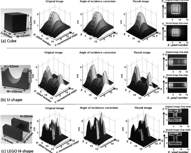
In the case of the scanning experimental setup (Fig.2.4/I.) the data was processed as follows: first the sensor raw output was compensated for offset and ambient light and converted to distance and labeled as ’original image’, then the angle of incidence correction method was used, and finally, the image is then scaled us- ing the normalized polynomial fit to create the ’result image’. After the scanning process, the outline and the surface of the detected objects was tried to be recre- ated. The first measured object was a red wooden block cube (Fig. 2.8/a). On the original image the effect of the smoothing in the scanning direction can be well distinguished that was much lower in case of the result image. The top view of the original and result images also can be observed on Fig. 2.8/a where the threshold function was set to 2 cm and the result is marked with white lines. In case of the original image it marked a 6×4 pixel sized area and in case of the result image it marked a 4×4 pixel array, where each pixel size was 8 mm (both in the
Figure 2.7: Measurement and simulation result of the sensor array of an object (placed 20 cm above) at different angles of incidence, with the assumption that the angle of incidence is 0◦ (in Eq. (2.1) cosθ was equal to 1). This could be corrected with an iterative method where an assumption for the angle of incidence could be given. As the third and fourth line show the simulated and measured distance after 3 iterations using this method highly improves the distance measurement.
x, y direction) suggesting that the scanned object dimensions were W = 32 mm, L = 32 mm.
The second scanned object was a solid wooden U-shaped block (Fig. 2.8/b).
The edges of the U-shape were smoothed because the object was not well aligned with the sensor grid. The middle curve was measured to be 5 mm smaller than the actual distance because of the deflection from the inner curve of the U-shape.
On the top view the side edges and the size of the object are visible. To outline the object, the surface cut was made near the ground at 1 cm. The outline of the object was marked successfully, as can be seen on the top view in Fig. 2.8/b.
The outline suggests that the dimensions of the object were W = 32 mm and L = 96 mm.
Figure 2.8: Results of the experimental setup I. (Fig.2.4/I.), where the (a),(b),(c), objects were placed under a x, y, z plotter table. Thex axis indicates the number of the pixels,yis the scanning direction (also marked with an arrow) and thez axis shows the distance in cm. The original image is made from the sensor row output after ambient light and offset compensation and conversion to distance. The result of the angle of incidence correction is presented. During the scanning process, as the sensor array moved closer to the measured object,light is also reflected from the side of the object causing false distance estimation and blurring the edges in the scanning direction. To sharpen these edges the images were scaled by their normalized polynomial fit creating the result image. The top view of each object shows the size of the object in case of the original image and result image where a threshold function was applied and the result is marked with white lines.
2.5.2.2 Surface trace
The sensor array capabilities for object surface-trace reconstruction were also tested using a shiny object (Fig. 2.4/c). As can be seen in Fig. 2.8/a where a cube was measured the object flat surface was successfully recreated except near the edges.
Also in Fig. 2.8/b, the real object can be recognized but the edges were blurred.
As a conclusion this sensor array was capable of creating surface-trace of objects but only in a limited way. To demonstrate these problems, an H shaped structure from red LEGO blocks was formed. The result of the scanning process can be seen in Fig.2.8/c. Since the surface of the LEGO was shiny, and the small joining parts on the top were scattering thus false peaks in the distance measurement appear.
Hence, the angle of incidence correction cannot be used as in this case the false peaks were even more increased. The main problems of the procedure were with the edges as there were deflection and scattering. As a consequence detailed objects were hard to capture. Also the surface of the object should be diffuse otherwise the effect of the scattering was higher. However, the outline of the object could still be recognized as the top view of the original image demonstrated.
2.5.2.3 Image registration
Three coin batteries (d = 20 mm, h = 5mm) were placed under the sensor array, two on each other and one next to those 2.9/(a). If a camera had been mounted to the robot feet an ideal output image would be 2.9/(b) (note that, from such a small distance, special fish-eye lenses and correction algorithms would be needed to produce such an image), where there are no additional information about the object high. The sensor low resolution image (8x8) can be seen in 2.9/(c). From such an image hard to make reliable decisions about any of the object’s properties.
By only making eight additional image (during the robot leg in motion) with the sensor array in each direction a higher resolution image can be created2.9/(d), where the object form, hight and width can be more clearly depicted. If a higher resolution is needed it can be achieved by using more sensors in the array or making smaller incrementation steps in each direction. Thus the time (how long it takes to create a registered image) and the number of sensors can be optimised.
With this method by using a low resolution sensor array obstacle detection can be made. The number of the registered and jointed images can be dynamically set based on the resolution needed, or it can be based on visual attention (if an object is detected than the number of images can be increased).
Figure 2.9: The previous version of the sensor array (describen in [4]) was attached to a bipedal robot [3] in order to detect obstacles under the robot feet (a). (b) shows an ideal case when a camera was attached to the robot feet and image was captured (note that, from such a small distance special fish-eye lenses and correction algorithms would be needed to produce such an image) (c) is the low resolution output of the 8x8 sensor array. Simulating the robot feet motion with the plotter table during its motion an extra 8 sensor measurement was made in each direction, and these were registered and joint together to produce a higher resolution image (d) where the object outline and the fact that the second object was higher can be depicted. 1
2.5.3 Mobile robot experiments
2.5.3.1 Landmark detection
Materials at the same distance but with different reflection properties could be used to mark objects or to code information, for example different kinds of shapes
can be drawn on the surface and could be used as landmarks for navigation.
A plus, a triangle, and a square shape were formed on the floor using 1.5 cm wide and 10 cm long white strips of masking tape. The robot was driven over each shape and the measurement result can be seen on Fig. 2.10. In case of the plus shape (Fig. 2.10/a) the edges were blurred but recognizable. The result could be improved by using wider strips, or by using a color that provides higher contrast to the background (floor). Fig. 2.10/b shows a triangle; the middle of the triangle was hardly captured because of the reflection from the side strips. The vertices of the triangle were missed as they were smaller than the pixel resolution. In the case of the square (Fig. 2.10/c) the corners gave higher responses than the straight parts. This was because the used white strip was somewhat transparent and the more layer were covering the more light was reflected. Thus at the corners where two strips are overlapping the given landmark reflects more light. This can also be observed with the other shapes as well.
Figure 2.10: Scan result of different landmarks. On the top are the pictures of the used landmarks and on the bottom the images created with the sensor array attached on a mobile robot.
1Image used with permission of Mikl´os Koller, the image was created as a part of his M.Sc degree under my supervision
2.5.3.2 Door-step detection
The PowerBot was driven over on a door step (phaseS1 − S2 in Fig.2.11/c). The two high responses visible in Fig. 2.11/a,b near to S2 were the highly reflective metal protectors on the edges, a wooden surface in between.
A longer scanning result (∼4 second) of a drive through process is shown in Fig. 2.11/b (each main phase is indicated in Fig. 2.11/c).
After the robot started to move the doorstep was detected before the front wheel reached it. As the front wheels got on the door step the distance between the ground and the sensor was increased thus less light was reflected to the sensor.
A straight motion was recorded until the rear wheels arrived to the door step and pushed the robot front down thus the distance between the ground and the sensor was decreased and more light was reflected to the sensor.
With this method the doorstep (or any obstacle) and each phase of a drive through process can be detected before the robot reaches, and based on the mea- sured sensor output it can be decided to stop the mobile robot or increase the speed to be able to go through the obstacle. It should be noted that precise (ma- terial independent) measurement could be done by using supplementary distance measurement sensor (for instance, ultrasound).
2.5.3.3 Map building (SLAM)
In a proof of the concept localization experiment, the PowerBot robot was driven on the linoleum floor of the laboratory. The measured data (part of a map) can be seen in Fig. 2.12/a. Shorter straight motion was also made in the same region; the sensor output is shown in Fig. 2.12/b. It could be easily depicted, with commonly used SLAM techniques, which part of the previously made motion was repeated and in this way the location of the robot could be estimated.
It should be noted that seeing the experimental results, the proposed measure- ment technique might give a possible solution for the problem of low cost SLAM at home or in industrial robotics. However, creating SLAM with a one row sensor array pattern matching would be too difficult without knowing the exact speed and orientation of the robot. This problem probably could be solved by extending the sensor array into 2D (8×8 or more), but this claim has to be supported by further experiments in the future.
Figure 2.11: The sensor array was mounted on a PowerBot type mobile robot front bumper and was directed to the ground, measurements were taken while the robot was moving. (a) shows the sensor output of a door-step while the PowerBot is driven over with a constant speed (phase S1 − S2 in (c)). The high peaks in the measurements are caused by the metal protectors on the door-step edges, and in between the wooden surface can be seen. (b) shows a drive through process where each phase of the drive through process can be recognized (the cross-section for each sensor value have been plotted on top of each other) and (c) indicates each phase. The robot started to move after S1, the edge of the door-step is detected at S2. After the sensor array got through the door-step there was a straight motion (between S2, S3) indicating higher sensor responses as the floor material was different in this room. At S3 the distance of the sensor array was increasing from the ground as the first wheels got on the door-step and lifted the front side of the mobile robot. S4 indicates when the back wheels reached the door-step and pushed the robot front down and after a straight motion in the new room could be observed S5.
Figure 2.12: (a) shows a scan result of part of a laboratory (covered with linoleum).
The changes in the raw output is caused by the color/contrast change in the ma- terial.(b) shows the result of a second scanning process on part of the same area.
By comparing the two images it can be identified which part of the motion was repeated (marked with white dotted line on (a)). This sensorial data could be used as supplementary data for creating SLAM.
2.6 Conclusion
In this chapter a novel infrared LED and photodiode based distance measurement array has been presented. The two main advantages of the system are the fast readout speed and high resolution in the distance measurement. Additionally, the array structure helps to improve the pixel resolution and also helps in the calcu- lation of the angle of incidence. The sensor array capabilities were examined for outline and surface-trace detection of various objects. The device has proved useful but with some limitations. One problem is the deflection that smooths the edges.
Furthermore, the reflected amount of light highly depends on the brightness of the object, but this could be improved by using a supplementary distance measurement sensor (e.g. US). Measurement results with a mobile robot were also presented. A door-step was successfully measured and each phase of the drive through process could be well distinguished. It was also shown that the developed sensor array was capable of detecting ground landmarks for navigation purposes. The measure- ment accuracy could be improved by using higher resolution sensor array (smaller distance between the infrared LED and photodiode) and more directional light source.
Although the presented solution may not be as accurate as for example laser scanners or camera systems are, normally low resolution data is enough for object detection, avoidance and classification tasks. Also in those environments where the operation speed is crucial and computation power has to be small a compromise has to be made between resolution and speed. This sensor array could be useful in many applications, for example in production lines for object classification or orientation detection, or in robot navigation (landmark detection), obstacle avoidance and detection and for SLAM in consumer and industrial robotics. The summary of the contributions are the following:
• a new solution has been given for object outline and surface trace detection with 8×1 LED-photodiode pair based sensor array
• resolution greater than the spacing between infrared LED and photodiode pairs has been achieved
• an iterative method has been described to calculate the angle of incidence for achieving more precise distance measurement
• mobile robot applications (landmark, doorstep (obstacle) detection) has been examined for localization purposes
As conclusion the following thesis points can be stated:
Thesis I.:
Object outline and surface trace detection using 3D imaging based a low resolution proximity array containing infra LEDs - photodiodes.
A: I have designed and implemented a low resolution infra LED - photodiode based proximity array. Using several photodiodes to detect the reflected light from each infra LED, an iterative method was developed to calculate the angle of incidence in case of flat objects with knownαi parameters, to achieve more precise distance measurement.
B: A new method has been given to decrease the smoothing effect at object edges during the sensor array motion.
C: I have demonstrated in mobile robot experiments that the sensor array is capa- ble of detecting on road localization landmarks and obstacles before crossing.
Published in: [1]
Chapter 3
Complaint 3D Tactile Sensor
3.1 Introduction
Robots today are already able to perform various tasks such as walking or dancing.
In a well modeled environment even without external sensorial feedback, they can already execute a number of tasks [14]. In an unstructured environment however, they must sense their surroundings and make contact with various objects. Equip today’s humanoid robots with an advanced grasp and manipulation capabilities are the ultimate goal. In order to create complicated manipulation tasks, tactile information is essential. The robot hand equipped with tactile sensors should be capable of detecting when contact occurred and should be able to identify shapes, object texture, forces and slippage. There are only a few tactile sensors available on the market and most of these sensors have a rigid structure. A typical single sensor type is the Force Sensing Resistor (FSR) available in many shapes and sizes (d=5 - 50mm). Larger matrix based sensor arrays are available from e.g. Tekscan.
Both of these are only capable of measuring normal forces.
The basic problem with these kind of sensors, as demonstrated byRussell [50], is that rigid tactile sensors provide little information for all but very flat and hard objects.
Compliant tactile sensors would allow the sensor surface to deform on the gripped object thus the contact area increased and the stability of the precision grip. And in case of power grasping the compliant surface would also help to share the forces on a bigger area. In many researches a soft material is placed on these rigid sensors to meet this need [51] but this solution makes the tactile inversion problem even harder.
A few articles describes compliant tactile sensors which are suitable to use on a robotic hand. One interesting fingertip tactile sensor is presented by Choi et al.
[52] using polyvinylidene fluoride (PVDF), and pressure variable resistor ink to de- tect normal forces as well as slip. Hellard et al. [53] shows a sensor array utilizes the properties of optical dispersion and mechanical compliance of urethane foam.
As a force is applied onto the urethane foam due to the compression the intensity of scattered radiation is increased and the photodetector output will change accord- ingly. The greatest advantages of this sensor are the easy manufacturing process, durability, scalability, low cost and having good sensitivity. However, covering a larger area with a dense sensor array (e.g 25 sensing points per square cm) on a robot hand is very hard to achieve. One reason for this is that the data produced by such an array is hard to process. The physical implementation of the wiring is even more challenging. Researchers try to create wireless solutions [54] or use op- tical methods to decrease the number of the wires [55]. Most of the optical tactile sensors utilize a CCD or CMOS camera to capture the deformation of a surface caused by external force [56] they are multitouch but their size and computation power makes it difficult to use on a robot hand yet. Another very clever solution is to place a six DOF force/torque sensor inside the fingertip [57, 58]. The applied force can be measured and the point of contact can be calculated on the whole surface of the fingertip [59].
Tactile sensors placed on a robot hand should not just sense the normal forces, but should also be able to detect the force incidence angle. Most of 3D sensors are MEMS based [60] and have already proven to be useful in detecting and identifying slippage and twisting motion [61]. However covering larger areas would be too difficult.
In this chapter, an easily scalable (fingertip or palm sized) 3D optical tactile sensor covered with a compliant surface is presented. The silicone rubber cover makes it prone to contact and will increase the grasp stability. A layer structured silicone cover is also presented to increase the noise performance and reduce the size. The presented sensor prototype is 35 mm in diameter and 30 mm high, and the point of contact, direction and magnitude of the applied force can be measured on the whole surface. The sensor output is analog and request only a minimal number of electrical component to connect to a microcontroller or to a PC. It has a robust structure with a respectable overload capability, high sensitivity (threshold 2g), high static load range (≥2000:1), and high speed operation (in KHz range).
3.2 Design concepts
The elastic deformation of a material is proportional to the applied force. If the compression of the material is measured and its Young modulus is known than the applied force can be calculated. In this way, the force measurement problem can be turned into a distance measurement problem.
To measure distance in a non contact way the traditional methods are the ultrasonic and optical solutions. The US sensor measures the time of flight (ToF) of the ultrasound signal emitted and reflected to the receiver. Today’s ultrasonic sensors have an average diameter of 15 mm and the minimal sensing distance of a few centimeters (3 cm). The most common offset-based Position Sensing Devices (PSD) such as Sharp GP series are a size of 44 mm x 13 mm with a minimal sensing distance of 4 cm (Model GP2D120, range 4-30 cm).
Unfortunately using these sensors would make the tactile sensor too large due to their dimensions and minimal sensing range. A possible solution could be to use infrared LED and photodiode pairs, arranged in a reflective configuration. The reason why this method is not frequently used for accurate distance measurements is that the reflected amount of light highly depends on the reflective properties of the sensed object surface thus material independent distance measurement is difficult to achieve. However, in this case, where the used elastic material properties are constant it can be used responsibly.
The tactile sensor surface should be prone to contact with any kind of object at any kind of angle. For this reason, the shape of its surface was chosen to be a hemisphere like. The sensor should also have a reliable overload capacity before permanent damage is caused. The dynamic range should be in KHz range in order to be able to detect vibration. The composed material should be durable and in-expensive with a repeatable sensor response with no (or minimal) hysteresis.
3.3 Sensor description
The base of the tactile sensor is composed of three photodiodes and an infrared LED. The photodiodes are placed around a circle at every 120◦ and an infrared LED is in the middle (Fig. 3.1/a). This is covered with a hollow elastic dome as a spherical interface, made form silicone rubber (RTV-2 type), that is fixed to the PCB (Fig. 3.1/b). The thickness of the dome will determine the range of measurement: the thinner it is, the more it will deform for a given load. The number of the used components and their size makes the sensor size easily scalable.
The sensor capabilities highly depend on the photodiodes amplification value, the photodiode sensitivity, infra LED power and the material of the cover to obtain an optimal solution their relation should be analyzed.
The optical measurement method helps to achieve a high dynamic range both, in the distance, and in the time domain. The sensor read out speed could be even in the MHz range, and as the output signal is analog the achieved resolution only depends on the used Analog to Digital Converter (ADC). The sensor structure is very durable, if the external force is greater than the maximum desired force applied onto the elastic dome, it can be deformed until it reaches the PCB level resulting in a respectable overload capacity. As the silicone cover material has elastic and viscoelastic properties after the force was released a relaxation period could be observed, which was proportional with the applied force, however to modell this phenomena is part of the future researches.
The basic mechanism of the 3D tactile sensor is that the amount of force mea- sured with the three separated photodiode are used to estimate tridirectional forces imposed on the sensor. The measurement principle is as follows: the infrared LED lights illuminate the inner structure of the dome. At no force, the reflected amount of light to each photodiode is equal. A force applied on the surface will result in deformation, on this region the surface of the dome will be closer to a given pho- todiode thus more light will be reflected to that sensor (Fig. 3.1/b).
For practical purposes, only three photo diodes were used in the first prototype.
As a result, the equations (Eq. 3.3) are only approximations as in this case the origin of the calculated axis is not in the center (on the infra LED), thus to measure the independent x,y force component, this offset must be taken into account. However, by using four photo diodes, each axis can be calculated as the difference of the two opposite photodiodes on one axis and in this case the origin will be in the middle of the infra LED without having an offset.
Figure 3.1: Schematic drawing of the tactile sensor, the three photodiodes are placed around on a circle at every 120◦ and an infrared LED is in the middle mounted on a PCB board (a). It is covered with an elastic hollow dome. A force applied on the elastic cover will result deformation (b). This deformation is proportional to the reflected light to the appropriate photodiode thus the applied force can be measured. The basic mechanism of the 3D tactile sensor is that the amount of force measured on the three separated pressure are used to estimate tridirectional forces imposed on the sensor. The proof of the concept version of the sensor is presented on (c), with the hollow elastic silicone cover (d) and the PCB (e).
The measurement of the three photodiodes (S1,S2,S3) could be used to estimate the normal (Fz) and the tangential force components (Fx,Fy) using the following equations:
Fx =k((S2−β2) + (S3−β3)
2 −(S1−β1)) (3.1)
Fy =k(S2 −β2)−(S3−β3)) (3.2)
Fz =k(
Pi=1
3 (Si−βi)
3 ) (3.3)
whereβi is composed of two values namely the sensor output without infrared light emission (sensor offset) and the sensor output with infrared light emission at no force applied (calibration value) and k is the spring constant (now it is taken to be one).
The used infrared LED (Model TSHF5210, Vishay Ltd, US) is driven by a mi- crocontroller (Model PIC24HJ32GP204, Microchip, US). While the infrared LED is on the photodiodes (Model BPW34, Vishay Ltd, US) outputs after amplification are converted to digital with a 24 bit ADC (Model ADS1258, TI, US) (but only 18 bit resolution is used where the two highest MSB is negligate thus the output representation is 16bit) and are sent to the PC via a USB port (Fig. 3.2).
The photodiode characteristic is non-linear, to be closer to the linear output in the measurement range the infrared LED current is set based on its output characteristic. Thus the photodiode output characteristic will have the highest change at the range where no load or maximal load applied. As the measuring method is optical the infra light illumination must be very stable. Although the infra LED is current controlled, illumination change during the system initialization could be observed, this was because of the temperature changing inside the LED caused by the current flow. Even so, as soon as the LED crystal reached its working temperature (∼1 min) the output signal became stable.
Figure 3.2: The data acquisition board and a connected tactile sensor prototype.
The board is capable of processing the signals of two sensors and it sends to the PC through USB port.
3.3.1 Theory of operation
In this section a short description will be given about the sensor simplified operation in 2D case. The inside of the semicircle is illuminated with a point light source (infra led) with an intensity of L from its middle point (origin), and the reflected amount of light is measured in two points (photo diodes) equally placed from the origin with a distance of DS (Fig.3.4).
Figure 3.3: Schematic drawing of the semicircle where in the origin is the point source (infra LED) and on two sides are the detectors SL, SR(photo diodes). The red lines represent the light rays from the point source, and with blue and black lines the reflected ray to the detectors are marked, r is the radius of the semicircle and DS is the detector distance of the origin.
Based on the inverse square law the light intensity at each point of the semicircle can be calculated:
LC(r) = L
πr (3.4)
wherer is the radius of the semicircle,C is the circumference andsis the length of the arc. Each point on the semicircle is taken as a new light source so to calculate the reflected amount of light to each photo diode (SL: photo diode left,SR: photo diode right). The inverse square low is used as well. The distance between the
photo diode and semicircle points can be expressed as:
DSR(α) =p
(rcos(α)−DS)2+ (rsin(α))2, α∈[0, π] (3.5) DSL(α) = p
(rcos(α) +DS)2+ (rsin(α))2, α∈[0, π], (3.6) where α is calculated in radian and can be expressed based on the length of the arc:
α = s
r (3.7)
Thus by using the inverse square low the intensity at each photo diode can be calculated using the following equations:
LSR = Z C2
0
L πr
1 πp
(rcos(sr)−DS)2+ (rsin(sr))2ds (3.8) LSL =
Z C2
0
L πr
1 πp
(rcos(sr) +DS)2+ (rsin(sr))2ds. (3.9) To simulate this model the equations were solved using numeric approximation in Matlab. The semicircle radius was set to r=30 mm and the light intensity to L=10W/sr with N number of rays. The number of rays were set to 18000 as in this case the simulation error settled at a reasonable level of 0.006%, so in the simulationαi goes from 0 to π with an increment ofπ/N but for practical reasons on the figures only 18 rays are plotted. The deformation was added to the model by overwriting the semicircle equation between two arbitrary angles. For example, by setting it from 60◦ to 120◦, they(αi) =y(αi−1) (where αi ∈[0, π]) the semicircle top will be flat as it can be seen in Fig.3.4/b. This method results that the original length of the semicircle arc will be changed, thus Eq. 3.7is no longer true. In case of deformation, the circumference can be calculated by summing the length of the arcs using the following equation:
C =
π
X
i=1
p(x(αi+ 1) +x(αi))2+ (y(αi+ 1) +y(αi))2 (3.10)
Using a different deformation factor the light intensity was measured at point SL and SR as it can be seen in Fig. 3.4/a. Without deformation both intensities
(LSL,LSR) are the same. If there is a deformation parallel with the ground (xaxis), then the intensity will be increased equally both in SL and SR. In case of side deformation the light intensity increases on the same side as the deformation was, thus it can be stated that the degree and direction of deformation is proportional with the measured light intensity at point SL and SR.
Figure 3.4: Deformation level of the semicircle at different direction of forces.
On the top of each figure, the measured intensity LSL, LSR is shown. (a) shows the initial state without deformation where LSL and LSR is equal. In (b) the deformation is parallel with thexaxis and bothLSL andLSRmeasures the highest intensity. (c) and (d) show the deformation from left and from right where the measured light intensity is higher at the deformation side.


![Figure 2.9: The previous version of the sensor array (describen in [4]) was attached to a bipedal robot [3] in order to detect obstacles under the robot feet (a)](https://thumb-eu.123doks.com/thumbv2/9dokorg/1311871.105514/36.892.117.737.158.695/figure-previous-version-sensor-describen-attached-bipedal-obstacles.webp)