An Optimal Mapping of Numerical Simulations of Partial Differential Equations to Emulated
Digital CNN-UM Architectures
Andr´ as Kiss
A thesis submitted for the degree of Doctor of Philosophy
Scientific adviser:
Zolt´ an Nagy Supervisor:
P´ eter Szolgay
Faculty of Information Technology P´ eter P´ azm´ any Catholic University
Budapest, 2011
I would like to dedicate this thesis to my beloved grandfathers.
Acknowledgements
It is not so hard to get a Doctoral Degree if you are surrounded with talented, motivated, optimistic, wise people who are not hesitating to give guidance if you get stuck and knowledge to pass through diffi- culties. There are two men who motivated me to continue my study after the university, and pushed me forward continuously to reach my humble goals. They know my path, because they already walked on it. This work could not have come into existence without the aid of my supervisor and mentor Professor Peter Szolgay and my adviser and friend Dr. Zolt´an Nagy.
I am also grateful to my closest collaborators for helping me out in tough situations, to Dr. Zsolt V¨or¨osh´azi, S´andor Kocs´ardi, Zolt´an Kincses, P´eter Sonkoly, L´aszl´o F¨uredi and Csaba Nemes.
I would further like to say thanks to my talented colleagues who con- tinuously suffer from my crazy ideas, and who not chases me away with a torch, especially to ´Eva Bank´o, Petra Hermann, Gergely So´os, Barna Hegyi, B´ela Weiss, D´aniel Szolgay, Norbert B´erci, Csaba Benedek, R´obert Tibold, Tam´as Pilissy, Gergely Trepl´an, ´Ad´am Fekete, J´ozsef Veres, ´Akos Tar, D´avid Tisza, Gy¨orgy Cserey, Andr´as Ol´ah, Gergely Feldhoffer, Giovanni Pazienza, Endre K´osa, ´Ad´am Balogh, Zolt´an K´ar´asz, Andrea Kov´acs, L´aszl´o Koz´ak, Vilmos Szab´o, Bal´azs Varga, Tam´as F¨ul¨op, G´abor Tornai, Tam´as Zsedrovits, Andr´as Horv´ath, Mikl´os Koller, Domonkos Gergelyi, D´aniel Kov´acs, L´aszl´o Laki, Mih´aly Radv´anyi, ´Ad´am R´ak, Attila Stubendek.
I am grateful to the Hungarian Academy of Sciences (MTA-SZTAKI) and P´eter P´azm´any Catholic University, where I spent my Ph.D.
years.
I am indebted to Katalin Keser˝u from MTA-SZTAKI, and various offices at P´eter P´azm´any Catholic University for their practical and official aid.
I am very grateful to my mother and father and to my whole family who always tolerated the rare meeting with me and supported me in all possible ways.
Contents
1 Introduction 1
1.1 Cellular Neural/Nonlinear Network . . . 4
1.1.1 Linear templates . . . 4
1.1.2 Nonlinear templates . . . 6
1.2 Cellular Neural/Nonlinear Network - Universal Machine . . . 7
1.3 CNN-UM Implementations . . . 9
1.4 Field Programmable Gate Arrays . . . 12
1.4.1 The general structure of FPGAs . . . 12
1.4.2 Routing Interconnect . . . 14
1.4.3 Dedicated elements, heterogenous structure . . . 20
1.4.4 Xilinx FPGAs . . . 22
1.4.4.1 Xilinx Virtex 2 FPGA . . . 22
1.4.4.2 Xilinx Virtex 5 FPGAs . . . 23
1.4.4.3 The capabilities of the modern Xilinx FPGAs . . 24
1.5 IBM Cell Broadband Engine Architecture . . . 26
1.5.1 Cell Processor Chip . . . 26
1.5.2 Cell Blade Systems . . . 32
1.6 Recent Trends in Many-core Architectures . . . 34
2 Mapping the Numerical Simulations of Partial Differential Equa- tions 35 2.1 Introduction . . . 35
2.1.1 How to map CNN array to Cell processor array? . . . 36
2.1.1.1 Linear Dynamics . . . 36
2.1.1.2 Nonlinear Dynamics . . . 45
i
2.1.1.3 Performance comparisons . . . 48
2.2 Ocean model and its implementation . . . 49
2.3 Computational Fluid Flow Simulation on Body Fitted Mesh Ge- ometry with IBM Cell Broadband Engine and FPGA Architecture 53 2.3.1 Introduction . . . 53
2.3.2 Fluid Flows . . . 54
2.3.2.1 Discretization of the governing equations . . . 55
2.3.2.2 The geometry of the mesh . . . 55
2.3.2.3 The First-order Scheme . . . 56
2.3.2.4 The Second-order Scheme . . . 59
2.3.2.5 Implementation on the Cell Architecture . . . 60
2.3.2.6 Implementation on Falcon CNN-UM Architecture 62 2.3.2.7 Results and performance . . . 63
2.3.3 Conclusion . . . 65
3 Investigating the Precision of PDE Solver Architectures on FP- GAs 69 3.1 The Advection Equation . . . 70
3.2 Numerical Solutions of the PDEs . . . 70
3.2.1 The First-order Discretization . . . 71
3.2.2 The Second-order Limited Scheme . . . 72
3.3 Testing Methodology . . . 72
3.4 Properties of the Arithmetic Units on FPGA . . . 74
3.5 Results . . . 79
3.6 Conclusion . . . 84
4 Implementing a Global Analogic Programming Unit for Emu- lated Digital CNN Processors on FPGA 87 4.1 Introduction . . . 87
4.2 Computational background and the optimized Falcon architecture 89 4.3 Implementation . . . 91
4.3.1 Objectives . . . 91
4.3.2 Implementation of GAPU . . . 94
4.3.3 Operating Steps . . . 97
4.4 The real image processing system . . . 98
4.5 An Example . . . 100
4.6 Device utilization . . . 102
4.7 Results . . . 105
4.8 Conclusions . . . 106
5 Summary of new scientific results 109 5.1 Uj tudom´´ anyos eredm´enyek (magyar nyelven) . . . 113
5.2 Application of the results . . . 118
5.2.1 Application of the Fluid Flow Simulation . . . 118
5.2.2 Examining the accuracy of the results . . . 118
5.2.3 The importance of Global Analogic Programming Unit . . 119
References 128
List of Figures
1.1 Location of the CNN cells on a 2D grid, where the gray cells are
the direct neighbors of the black cell . . . 4
1.2 The output sigmoid function . . . 5
1.3 Zero- (a) and first-order (b) nonlinearity . . . 7
1.4 The architecture of the CNN Universal Machine, the extended CNN nucleus and the functional blocks of the GAPU . . . 8
1.5 General architecture of the programmable logic block . . . 13
1.6 Programmable I/O architecture . . . 15
1.7 Basic programmable switches . . . 16
1.8 Symmetrical wiring . . . 17
1.9 Cellular wiring . . . 18
1.10 Row-based wiring . . . 19
1.11 IBM PowerPC405 processor integration on Xilinx FPGA . . . 21
1.12 Block diagram of the Cell processor . . . 27
1.13 Block diagram of the functional units of the PowerPC Processor Element . . . 28
1.14 Block diagram of the Synergistic Processor Element . . . 30
1.15 IBM Blade Center QS20 architecture . . . 33
2.1 Generation of the left neighborhood . . . 38
2.2 Rearrangement of the state values . . . 38
2.3 Results of the loop unrolling . . . 39
v
2.4 Performance of the implemented CNN simulator on the Cell ar- chitecture compared to other architectures, considering the speed of the Intel processor as a unit in both linear and nonlinear case (CNN cell array size: 256×256, 16 forward Euler iterations, *Core 2 Duo T7200 @2GHz, **Falcon Emulated Digital CNN-UM imple- mented on Xilinx Virtex-5 FPGA (XC5VSX95T) @550MHz only
one Processing Element (max. 71 Processing Element). . . 40
2.5 Intruction histogram in case of one and multiple SPEs . . . 41
2.6 Data-flow of the pipelined multi-SPE CNN simulator . . . 43
2.7 Instruction histogram in case of SPE pipeline . . . 44
2.8 Startup overhead in case of SPE pipeline . . . 44
2.9 Speedup of the multi-SPE CNN simulation kernel . . . 45
2.10 Comparison of the instruction number in case of different unrolling 47 2.11 Performance comparison of one and multiple SPEs . . . 48
2.12 The computational domain . . . 56
2.13 Local store buffers . . . 61
2.14 Data distribution between SPEs . . . 62
2.15 Number of slices in the arithmetic unit . . . 64
2.16 Number of multipliers in the arithmetic unit . . . 65
2.17 Number of block-RAMs in the arithmetic unit . . . 66
2.18 Simulation around a cylinder in the initial state, 0.25 second, 0.5 second and in 1 second . . . 67
3.1 Error of the 1st order scheme in different precision with 104 grid resolution . . . 75
3.2 The arithmetic unit of the first order scheme . . . 76
3.3 The arithmetic unit of the second order scheme . . . 77
3.4 Structure of the system with the accelerator unit . . . 78
3.5 Number of slices of the Accelerator Unit in different precisions . . 78
3.6 Error of the 1st order scheme in different precisions and step sizes using floating point numbers . . . 80
3.7 Error of the 2nd order scheme in different precisions and step sizes using floating point numbers . . . 81
3.8 Error of the 1st order scheme in different precisions and step sizes using fixed-point numbers . . . 82 3.9 Comparison of the different type of numbers and the different dis-
cretization . . . 83 4.1 The structure of the general Falcon processor element is optimized
for GAPU integration. Main building blocks and signals with an additional low-level Control unit are depicted. . . 90 4.2 Structure of the Falcon array based on locally connected processor
elements. . . 92 4.3 Detailed structure of the implemented experimental system (all
blocks of GAPU are located within the dashed line). . . 95 4.4 Block diagram of the experimental system. The embedded GAPU
is connected with Falcon and Vector processing elements on FPGA. 99 4.5 Results after some given iteration steps of the black and white
skeletonization. . . 101 4.6 Number of required slices in different precision . . . 103 4.7 Number of required BlockRAMs in different precision . . . 104
List of Tables
2.1 Comparison of different CNN implementations: 2GHz CORE 2 DUO processor, Emulated Digital CNN running on Cell processors and on Virtex 5 SX240T FPGA, and Q-EYE with analog VLSI chip 49 2.2 The initial state, and the results of the simulation after a couple
of iteration steps. Where the x- and y-axis models 1024km width ocean (1 untit is equal to 2.048km). . . 52 2.3 Comparison of different CNN ocean model implementations: 2GHz
CORE 2 DUO processor, Emulated Digital CNN running on Cell processors . . . 53 2.4 Comparison of different hardware implementations . . . 68 4.1 Comparison of a modified Falcon PE and the proposed GAPU
in terms of device utilization and achievable clock frequency. The configuration of state width is 18 bit. (The asterisk denotes that in Virtex-5 FPGAs, the slices differently organized, and they contain twice as much LUTs and FlipFlops as the previous generations). . 105 4.2 Comparison of the different host interfaces. . . 106
ix
List of Abbreviations
ALU Arithmetic Logic Unit
ASIC Application-specific Integrated Circuit ASMBL Advanced Silicon Modular Block BRAM Block RAM
CAD Computer Aided Design
CBEA Cell Broadband Engine Architecture CFD Computational Fluid Dynamics CFL Courant-Friedrichs-Lewy
CISC Complex Instruction Set Computer CLB Configurable Logic Blocks
CNN Cellular Neural/Nonlinear Network
CNN-UM Cellular Neural/Nonlinear Network - Universal Machine DMA Direct Memory Acces
DSP Digital Signal Processing EIB Element Interconnect Bus FIFO Firs In First Out
FIR Finite-impulse Response
xi
FPE Falcon Processing Element
FPGA Field Programmable Gate Array FPOA Field Programmable Object Array FSR Full Signal Range
GAPU Global Analogic Programming Unit IPIF Intellectual Property Interface
ITRS International Technology Roadmap for Semiconductors LUT Look-Up Table
MAC Multiply - accumulate Operation MIMD Multiple Instruction Multiple Data MPI Message Passing Interface
OPB On-Chip Peripheral Bus PDE Partial Differential Equation PE Processing Element
PPC PowerPC
PPE Power Processor Element
RISC Reduced Instruction Set Computer SDK Software Development Kit
SIMD Single Instruction Multiple Data SLR Super Logic Region
SPE Synergistic Processor Element SSI Stacked Silicon Interconnect
TFLOPS Tera Floating Point Operations Per Second VHDL VHSIC hardware description language
VLIW Very Long Instruction Word VLSI Very-large-scale integration VPE Vector Processing Element
Chapter 1 Introduction
Due to the rapid evolution of computer technology the problems on many pro- cessing elements, which are arranged in regular grid structures (array processors), become important. With the large number of the processor cores not only the speed of the cores but their topographic structure becomes an important issue.
These processors are capable of running multiple tasks in parallel. In order to make an efficiently executed algorithm, the relative distance between two neigh- boring processing elements should be taken into consideration. In other words it is the precedence of locality phenomenon. This discipline requires the basic operations to be redesigned in order to work on these hardware architectures efficiently.
In the dissertation solutions for solving hard computational problems are searched, where the area and dissipated power is minimal, the number of im- plemented processor, the speed and the memory access are maximal. A solution is searched within this parameter space for an implementation of a partial differ- ential equation, and the solution is optimized for some variable of this parameter space (e.g.: speed, area, bandwidth). The search space will be always limited by the special properties of the hardware environment.
There are several known problems, which cannot be computed in real time with the former resources, or just very slowly. The aim of the research is the examination of these hard problems. As an example a fluid flow simulation is going to be analyzed, and a hardware implementation for the problems is going to be introduced.
1
The motivation of the dissertation is to develop a methodology for solving partial differential equations, especially for liquid and gas flow simulations, which helps to map these problems optimally into inhomogenous and reconfigurable architectures. To reach this goal two hardware platforms as experimental frame- work were built up, namely the IBM Cell Broadband Engine Architecture and the Xilinx Field Programmable Gate Array (FPGA) as reconfigurable architecture.
After the creation of the framework, which models fluid flow simulations, it is mapped to these two architecture which follows different approach (see Chapter 2). To fully utilize the capabilities of the two architecture several optimization procedure had to performed. Not only the structure of the architectures are taken into consideration, but the computational precision too (introduced in Chapter 3). It is important to examine the precision of the arithmetic unit on FPGA, because significant speedup or lesser area requirement and power dissipation can be achieved. With the investigation of the computational precision, the decision can be taken, wether the problem fits onto the selected FPGA or not. It relies mainly on the number of operations in the arithmetic unit. To get a complete, standalone machine, the processing element on FPGA should be extended with a control unit (it is going to e introduced in Chapter 4).
The IBM Cell processor represents a bounded architecture, which builds up from heterogeneous processor cores. From the marketing point of view, the Cell processor failed, but its significant innovations (e.g.: heterogeneous processor cores, ring bus structure) can be observed in todays modern processors (e.g.:
IBM Power 7 [13], Intel Sandy Bridge [14]). According to the special requirement of the processor, vectorized datas were used which composed of floating point numbers. For the development of the software the freely available IBM software development kit (SDK) with C programming language was used.
Xilinx FPGAs are belonging to the leading reconfigurable computers since a while. Due to the fast Configurable Logic Blocks (CLB) and to the large number of interconnections arbitrary circuits can be implemented on them. In order to accelerate certain operations, dedicated elements (e.g.: digital signal processing (DSP) blocks) are available on the FPGA. The FPGA’s CLB and DSP can be treated like different type of processors which can handle different operations efficiently. Due to the configurable parameters of the FPGA the processed data
can be represented in arbitrary type and size. During the research fixed point and floating point number arithmetic units with different mantissa width were investigated in order to find the optimal precision for a qualitative good result.
During the implementation process I used the Xilinx Foundation ISE softwares with VHSIC hardware description language (VHDL) language. For the software simulation I used the MentorGraphics Modelsim SE software.
The Chapter 1 is built up as follows. First the CNN paradigm is introduced.
It is capable to solve complex spatio-temporal problems. The standard CNN cell should be extended with a control unit and with memory units in order to get an universal machine, which is based on the stored programmability (the extension is introduced in Chapter 4). Several studies proved the effectiveness of the CNN-UM solution of different PDEs [15, 16]. After the previous section several implementations of the CNN-UM principle are listed. The emulated dig- ital CNN-UM is a reasonable alternative to solve different PDEs. It has mixed the benefits of the software simulation and the analog solution. Namely the high configurability and the precision of the software solution and the high computing speed of the analog solution. In the later Chapters the CNN simulation kernel is going to be introduced on the IBM Cell processor and on the FPGA. In order to get the reader a clear understanding from the framework a brief introduction of the hardware specifications are presented. The final section is an outlook of the recent trends in many core systems.
1.1 Cellular Neural/Nonlinear Network
The basic building blocks of the Cellular Neural Networks, which was published in 1988 by L. O. Chua and L. Yang [17], are the uniform structured analog processing elements, the cells. A standard CNN architecture consists of a rectangular 2D- array of cells as shown in Figure (1.1). With interconnection of many 2D arrays it can be extended to a 3-dimensional, multi-layer CNN structure. As it is in organic structures the simplest way to connect each cell is the connection of the local neighborhood via programmable weights. The weighted connections of a cell to its neighbors are called the cloning template. The CNN cell array is programmable by changing the cloning template. With the local connection of the cells difficult computational problems can be solved, like modeling biological structures [18] or the investigation of the systems which are based on partial differential equations [19].
Figure 1.1: Location of the CNN cells on a 2D grid, where the gray cells are the direct neighbors of the black cell
1.1.1 Linear templates
The state equation of the original Chua-Yang model [17] is as follows:
˙
xij(t) = −xij+ X
C(kl)∈Nr(i,j)
Aij,klykl(t) + X
C(kl)∈Nr(i,j)
Bij,klukl+zij (1.1)
where ukl, xij, and ykl are the input, the state, and the output variables. A and B matrices are the feedback and feed-forward templates, and zij is the bias term.
Nr (i,j) is the set of neighboring cells of the (i,j)th cell. The output yij equation of the cell is described by the following function (see Figure 1.2):
yij =f(xij) = |xij + 1| − |xij −1|
2 =
1 xij(t)>1 xij(t) −1≤xij(t)≤1
−1 xij(t)<−1
(1.2)
V xij f(V xij )
1
1
-1 -1
Figure 1.2: The output sigmoid function
The discretized form of the original state equation (1.1) is derived by using the forward Euler form. It is as follows:
xij(n+ 1) = (1−h)xij(n)+
+h P
C(kl)∈Nr(i,j)
Aij,klykl(n) + P
C(kl)∈Nr(i,j)
Bij,klukl+zij
!
(1.3)
In order to simplify computation variables are eliminated as far as possible (e.g.:
combining variables by extending the template matrices). First of all, the Chua- Yang model is changed to the Full Signal Range (FSR) [20] model. Here the state and the output of the CNN are equal. In cases when the state is about to go to saturation, the state variable is simply truncated. In this way the absolute value of the state variable cannot exceed +1. The discretized version of the CNN state
equation with FSR model is as follows:
xij(n+ 1) =
1 if vij(n)>1 vij(k) if |vij(n)| ≤1
−1 if vij(n)<−1 vij(n) = (1−h)xij(n)+
+h P
C(kl)∈Nr(i,j)
Aij,klxkl(n)+ P
C(kl)∈Nr(i,j)
Bij,klukl(n) +zij
!
(1.4)
Now the x and y variables are combined by introducing a truncation, which is simple in the digital world from computational aspect. In addition, the h and (1-h) terms are included into the A and B template matrices resulting templates A, ˆˆ B.
By using these modified template matrices, the iteration scheme is simplified to a 3×3 convolution plus an extra addition:
vij(n+ 1) = X
C(kl)∈Nr(i,j)
Aˆij,klxkl(n) +gij (1.5a) gij = X
C(kl)∈Nr(i,j)
Bˆij,klukl+hzij (1.5b)
If the input is constant or changing slowly, gij can be treated as a constant and should be computed only once at the beginning of the computation.
1.1.2 Nonlinear templates
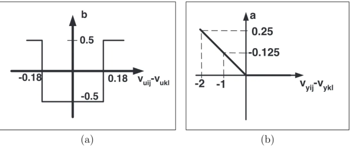
The implementation of nonlinear templates are very difficult on analog VLSI and quite simple on emulated digital CNN. In some interesting spatio-temporal prob- lems (Navier-Stokes equations) the nonlinear templates (nonlinear interactions) play key role. In general the nonlinear CNN template values are defined by an arbitrary nonlinear function of input variables (nonlinear B template), output variables (nonlinear A template) or state variables and may involve some time delays. The survey of the nonlinear templates shows that in many cases the nonlinear template values depend on the difference of the value of the currently processed cell (Cij) and the value of the neighboring cell (Ckl). The Cellular Wave Computing Library [21] contains zero- and first-order nonlinear templates.
-0.5 0.18 -0.18
0.5 b
v uij -v ukl v yij -v ykl 0.25
-0.125 -2 -1
a
(a) (b)
Figure 1.3: Zero- (a) and first-order (b) nonlinearity
In case of the zero-order nonlinear templates, the nonlinear functions of the template contains horizontal segments only as shown in Figure 1.3(a). This kind of nonlinearity can be used, e.g., for grayscale contour detection [21].
In case of the first-order nonlinear templates, the nonlinearity of the template contains straight line segments as shown in Figure 1.3(b). This type of nonlin- earity is used, e.g., in the global maximum finder template [21]. Naturally, some nonlinear templates exist in which the template elements are defined by two or more nonlinearities, e.g., the grayscale diagonal line detector [21].
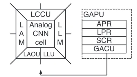
1.2 Cellular Neural/Nonlinear Network - Uni- versal Machine
If we consider the CNN template as an instruction, we can make different al- gorithms, functions from these templates. In order to run these algorithms ef- ficiently, the original CNN cell has to be extended (see Figure 1.4) [22]. The extended architecture is the Cellular Neural/Nonlinear Network - Universal Ma- chine (CNN-UM). According to the Turing-Church thesis in case of the algo- rithms, which are defined on integers or on a finite set of symbols, the Turing Machine, the grammar and the µ- recursive functions are equivalent. The CNN- UM is universal in Turing sense because every µ - recursive function can be computed on this architecture.
Analog CNN
cell L
A M
L L M LCCU
LAOU LLU
GAPU APR LPR SCR GACU
Figure 1.4: The architecture of the CNN Universal Machine, the extended CNN nucleus and the functional blocks of the GAPU
In order to run a sequence of templates, the intermediate results should be stored localy. Local memories connected to the cell store analog (LAM: Local Analog Memory) and logic (LLM: Local Logical Memory) values in each cell.
A Local Analog Output Unit (LAOU) and a Local Logic Unit (LLU) perform cell-wise analog and logic operations on the local (stored) values. The LAOU is a multiple-input single output analog device. It combines local analog values into a single output. It is used for analog addition, instead of using the CNN cell for addition. The output is always transferred to one of the local memories. The Local Communication and Control Unit (LCCU) provides for communication be- tween the extended cell and the central programming unit of the machine, across the Global Analogic Control Unit part of the Global Analogic Programming Unit (GAPU).
The GAPU is the ”conductor” of the whole analogic CNN universal machine, it directs all the extended standard CNN universal cells. The GAPU stores, in digital form, the sequence of instructions. Before the computations, the LCCU receives the programming instructions, the analog cloning template values A, B, z, the logic function codes for the LLU, and the switch configuration of the cell specifying the signal paths. These instructions are stored in the registers of the GAPU. The Analog Program Register (APR) stores the CNN templates,
the Logic Program Register (LPR) stores the LLU functions and the Switch Configuration Register (SCR) contains the setting of switches of an elementary operation of CNN cell.
1.3 CNN-UM Implementations
Since the introduction of the CNN Universal Machine in 1993 [22] several CNN- UM implementations have been developed. These implementations are ranged from the simple software simulators to the analog VLSI solutions.
The software simulator program (for multiple layers) running on a PC cal- culates the CNN dynamics for a given template by using one of the numerical methods either by a gray-scale code or a black and white image and can simulate the CNN dynamics for a given sequence of templates. The software solutions are flexible, with the configuration of all the parameters (template sizes, accuracy, etc.), but they are insufficient, considering the performance of computations.
The fastest CNN-UM implementations are the analog/mixed-signal VLSI (Very Large Scale Integration) CNN-UM chips [23], [20], [24]. The recent arrays contain 128 ×128 and 176×144 processing elements [25], [24]. Speed and dissipation advantage are coming from the operation mode. The solution can be derived by running the transient. The drawback of this implementation is the limited accu- racy (7-8 bit), noise sensitivity (fluctuation of the temperature and voltage), the moderate flexibility, the number of cells is limited (e.g., 128×128 on ACE16k, or 176×144 on eye-RIS), their cost is high, moreover the development time is long, due to the utilization of full-custom VLSI technology.
It is obvious that for those problems which can be solved by the analog (ana- logic) VLSI chips, the analog array dynamics of the chip outperform all the software simulators and digital hardware emulators.
The continuous valued analog dynamics when discretized in time and values can be simulated by a single microprocessor, as shown in the case of software simulators. Emulating large CNN arrays needs more computing power. The performance can be improved by using emulated digital CNN-UM architectures where small specialized processor cores are implemented. A special hardware
accelerator can be implemented either on multi-processor VLSI ASIC digital em- ulators (e.g CASTLE) [26], on DSP-, SPE-, and GPU-based hardware accelerator boards (e.g. CNN-HAC [27], Cell Broadband Engine Architecture [28], Nvidia Cuda [29], respectively), on FPGA-based reconfigurable computing architectures (e.g. FALCON [30]), as well. Generally, they speed up the software simulators, to get higher performance, but they are slower than the analog/mixed-signal CNN-UM implementations.
A special Hardware Accelerator Board (HAB) was developed for simulating up to one-million-pixel arrays (with on-board memory) with four DSP (16 bit fixed point) chips. In fact, in a digital HAB, each DSP calculates the dynamics of a partition of the whole CNN array. Since for the calculation of the CNN dynamics a major part of DSP capability is not used, special purpose chips have been developed.
The first emulated-digital, custom ASIC VLSI CNN-UM processor – called CASTLE.v1 – was developed in MTA-SZTAKI in Analogical and Neural Com- puting Laboratory between 1998 and 2001 for processing binary images [26], [31].
By using full-custom VLSI design methodology, this specialized systolic CNN array architecture greatly reduced the area requirements of the processor and makes it possible to implement multiple processing elements (with distributed ALUs) on the same silicon die. The second version of the CASTLE processor was elaborated with variable computing precision (1-bit ’logical’ and 6/12-bit
’bitvector’ processing modes), its structure can be expanded into an array of CASTLE processors. Moreover, it is capable of processing 240×320-sized images or videos at 25fps in real-time with low power dissipation (in mW range), as well. Emulated-digital approach can also benefit from scaling-down by using new manufacturing technologies to implement smaller and faster circuits with reduced power dissipation.
Several fundamental attributes of the Falcon architecture [30] are based on CASTLE emulated-digital CNN-UM array processor architecture. However, the most important features which were greatly improved in this FPGA-based im- plementation are the flexibility of programming, the scalable accuracy of CNN computations, and configurable template size. Therefore, the majority of these
modifications increased the performance. In case of CASTLE an important draw- back was that its moderate (12-bits) precision is enough for image processing but not enough for some applications require more precise computations. More- over, the array size is also fixed, which makes difficult to emulate large arrays, especially, when propagating cloning templates are used. To overcome these lim- itations configurable hardware description languages and reconfigurable devices (e.g. FPGA) were used to implement the FALCON architecture by employing rapid prototyping strategy [32]. This made it possible to increase the flexibil- ity and create application optimized processor configurations. The configurable parameters are the following:
• bit width of the state-, constant-, and template-values,
• size of the cell array,
• number and size of templates,
• number and arrangement of the physical processor cores.
1.4 Field Programmable Gate Arrays
Using reconfigurable computing (RC) and programmable logic devices for accel- erating execution speed is derived from the late 1980, at the same time with the spread of the Field Programmable Gate Array (FPGA) [33]. The innovative pro- gression of the FPGAs – which can be configured infinitely many times – lead the developments in a new line. With the help of these devices almost as many hardware algorithms can be implemented as software algorithms on conventional microprocessors.
The speed advantage of the hardware execution on FPGAs, which is practi- cally 10-100 times faster compared to the equivalent software algorithms, sparked the interest of developers attention who are working with digital signal processors (DSP) and with other hard computational problems. The RC developers realized the fact, that with FPGAs a significant performance gain can be achieved in cer- tain applications compared to the microprocessors, mainly in those applications which requires individual bit widths and high instruction-level parallelism. But the most important argument with the FPGA is the following: the commercially available devices evolves according to Moore’s law, the FPGA, which contains a large number of SRAMs and regularly placed logical blocks, scales with the ITRS (International Technology Roadmap for Semiconductors) memory roadmap [34].
Often they are the frontrunners in the development and in the application of new manufacturing technologies. For that reason, the reconfigurable devices evolves technically faster than the microprocessors.
1.4.1 The general structure of FPGAs
The FPGA, as reconfigurable computing architecture, builds up from regularly arranged logic blocks in two-dimension. Every logic block contains a Look-Up Table (LUT), which is a simple memory and can implement an arbitrary n-input logical function. The logic blocks are communicating with each other via pro- grammable interconnect networks, which can be neighboring, hierarchical and long-line interconnections. The FPGA contains I/O blocks too, which interfaces the internal logic blocks to the outer pads. The FPGAs evolves from the ini- tial homogenous architectures to todays heterogenous architectures: they are
containing on-chip memory blocks and DSP blocks (dedicated multipliers, and multiply/accumulator units).
Despite the fact that there are many FPGA families, the reconfigurable com- puters are exclusively SRAM programmable devices. That means, the configu- ration of the FPGA, the code as a generated ’bitfile’ – which defines the device implemented algorithm – stored in an on-chip SRAM. With the loading of the configurations into the SRAM memory different algorithms can be executed ef- ficiently. The configuration defines the logic function, which is computed by the logic blocks and the interconnection-pattern.
From the mid 1980 the FPGA designers developed a number of programmable logic structures into this architecture. The general structure is shown in Figure 1.5. This basic circuit contains programmable combination logic, synchronous flip-flop (or asynchronous latch) and some fast carry logic, for decreasing the need for area and delay dependency during the implementation. In this case the output can be chosen randomly: it can be a combination logic, or flip-flop. It can be also observed, that certain configuration uses memory for choosing the output for the multiplexer.
Figure 1.5: General architecture of the programmable logic block
There are a number of design methodology for the implementation of the combinational logic in the configurable logic block. Usually the configurable combinational logic is implemented with memory (Look-Up Table, LUT), but there are several architectures which uses multiplexers and logical gates instead of memories. In order to decrease the trade-offs generated by the programmable
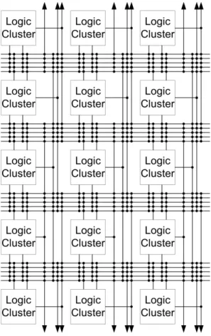
interconnections, in case of many reconfigurable FPGA architectures, the logical elements are arranged into clusters with fast and short-length wires. By using fast interconnects of clusters more complex functions with even more input can be implemented. Most LUT based architecture uses this strategy to form clusters with two ore more 4 or 6 input logical elements, which are called configurable logic block (CLB) in case of Xilinx FPGAs.
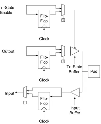
Basically the I/O architecture is the same in every FPGA family (see Fig- ure 1.6). Mainly a tri-state buffer belongs to the output and an input buffer to the input. One by one, the tri-state enable signal, the output signal and the input signal can be registered and un-registered inside the I/O block, which depends on the method of the configuration. The latest FPGAs are extended with many new possibilities, which greatly increased the complexity of the basic structure.
For example the Xilinx Virtex-6 latest I/O properties are the following:
• Supports more than 50 I/O standards with properties like the Digitally controlled impedance (DCI) active termination (for eliminating termination resistance), or the flexible fine-grained I/O banking,
• Integrated interface blocks for PCI Express 2.0 designs,
• Programmable input delays.
1.4.2 Routing Interconnect
Similarly to the structure of the logical units, the FPGA developers designed several solutions for interconnections. Basically the interconnections can be found within the cluster (for generating complex functions) and out of the cluster too.
For that reason, the important properties of a connection are the following: low parasitic resistance and capacitance, requires a small chip area, volatility, re- programmability and process complexity. Modern FPGAs are using two kind of connection architectures, namely the antifuse and the memory-based architecture.
The main property of the antifuse technology is its small area and low par- asitic resistance and capacitance. It barriers the two metal layer with a non- conducting amorphous silicon. If we want to make it conductive, we have to
Figure 1.6: Programmable I/O architecture
apply an adequate voltage to change the structure of the crystal into a low re- sistance polycrystalline silicon-metal alloy. The transformation could not turned back and that is why it can be programmed only once. This technology is applied by Actel [35] and QuickLogic [36].
There are several memory based interconnection structure, which are com- monly used by the larger FPGA manufacturers. The main advantage of these structures over the antifuse solution is the reprogrammability. This property gives the chance to the architecture designers to make rapid development of the architectures cost efficiently. The SRAM-based technology for FPGA configura- tion is commonly used by Xilinx [37] and Altera [38]. It contains 6 transistors, which stores the state of the interconnection. It has a great reliability and stores its value until the power is turned off.
Three kind of basic building blocks are used in the structure of the pro- grammable interconnections: multiplexor, pass transistor and tri-state buffer (see Figure 1.7).
Figure 1.7: Basic programmable switches
Usually multiplexers and pass transistors are used for the interconnections of the internal logical elements and all of the above are used for the external routing. (The use of the two, eight or more input multiplexer – depending on the complexity of the interconnections – is popular among the FPGAs.) The reason of the wiring inside of a logical cluster is follows:
• implementation of low delay interconnections between the elements of the clusters,
• to develop a more complex element using the elements of the clusters,
• non-programmable wiring for transferring fast carry bits for avoiding the extra delays when programmable interconnections (routing) are used.
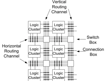
There are three main implementations for the global routing (which are used by the Xilinx by their FPGA family): row-based, symmetric (island) type and cellular architecture. Modern FPGA architectures are using significantly complex routing architectures, but their structures are based on these three.
In case of the symmetric routing architecture the logical clusters are sur- rounded by segmented horizontal and vertical wiring channels, which can be seen in Figure 1.8.
Figure 1.8: Symmetrical wiring
Every cluster connects to the channels via ”connection box” and every seg- ment in the routing can be interconnected to each other through a ”switch box”.
The main property of this architecture is that the interconnection is made by seg- mented wires. This structure can be found on many Xilinx FPGA: furthermore Xilinx provides variable lengths for the segments and it provides the clusters with local connections for improving the efficiency of the architecture.
The main difference between the cellular routing architecture and the sym- metrical architecture is that the densest interconnections are taking place local between the logical clusters and only a few (if there is any) longer connections exists (e.g.: Xilinx XC6200, see Figure 1.9).
Figure 1.9: Cellular wiring
In most cases this architecture is used in fined grained FPGAs, where the clus- ters are relatively simple and usually are containing only one logical element. In order to make the routing process more effective, these logical cells are designed in such way, that they may take part of the routing network between other log- ical elements. The main drawbacks of the cellular routing architecture are the followings:
• The combination pathways, which connects not only the neighborhood, may have a huge delay.
• In case of CAD (Computer Aided Design) tools, there occurs significant problem during the efficient placement of the circuit elements and the wiring of the circuit of the architecture (place & routing).
• The area and delay requirements of the fine grained architecture are sig- nificant compared to the number of logical element and routing resource
requirements for an algorithm implementation.
The importance of the last factor can be reduced if pipelining technique is used, which provides a continuous operation of the arithmetic unit.
The third type is the row-based routing architecture which can be seen in Figure 1.10.
Figure 1.10: Row-based wiring
This type is mainly used in the not reprogrammable FPGA (called ”one-time programmable FPGA”), that is why it is used less in todays reconfigurable sys- tems. It uses horizontal interconnections between two logical cluster. As the figure shows there are several vertical interconnections for connecting row-based channels. The row-based architecture uses segmented wires between routing chan- nels for decreasing the delays of the short interconnections.
1.4.3 Dedicated elements, heterogenous structure
In advanced FPGAs specialized blocks were also available. These blocks (e.g.: em- bedded memory, arithmetic unit, or embedded microprocessor) are implemented because they are commonly used elements, therefore the specialized blocks are using less general resources from the FPGA. The result is a highly heterogenous structure.
The memory is a basic building block of the digital system. Flip-flops can be used as a memory, but it will not be efficient in case of storing large amount of data. Firstly in case of Xilinx XC4000 FPGA were the LUTs enough flexible to use it as an asynchronous 16×1 bit RAM. Later it evolved to use as a dual-ported RAM or as a shift register. These clusters can be arranged in a flexible way to implement larger bit-width or deeper memory. E.g.: In case of a 4Kb on-chip RAM on Xilinx Virtex FPGA can be defined in the following hierarchical way:
4096×1, 2048×2, 1024×4, 512×8, 256×16.
Among the adders, which builds up from logical elements, in FPGA we can use embedded multipliers, or Digital Signal Processing (DSP) blocks like separate, dedicated resources. The DSP block can make addition, subtraction, multiplica- tion or multiply-accumulate (MAC) operation. The solving of a MAC operation in one clock cycle can be useful for finite-impulse response (FIR) filtering (which occurs in many DSP applications).
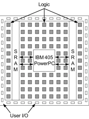
The FPGA manufacturers are integrating complete dedicated microproces- sors into their devices in order to implement low bandwidth and/or complex controlling functions. With this capability (nearly) fully embedded systems can be implemented on the FPGA. The embedded processor can be found on Xil- inx Virtex-II Pro, on Xilinx Virtex-4 and on Xilinx Virtex-5 FPGA. The Xilinx integrates dedicated hard processor cores (e.g.: IBM PowerPC405) into their de- vices (see Figure 1.11). These embedded processors are connected with on-chip SRAMs. That means without the configuration of the FPGA it can not make any useful work.
Figure 1.11: IBM PowerPC405 processor integration on Xilinx FPGA
1.4.4 Xilinx FPGAs
Xilinx FPGAs are belonging to the leading reconfigurable computers long ago.
Due to the fast Configurable Logic Blocks (CLB) and the large number of in- terconnections arbitrary circuits can be implemented on it. In order to acceler- ate certain operations dedicated elements (e.g.: digital signal processing (DSP) blocks) are available on the FPGA. Throughout the dissertation all the used FPGA platforms are made by Xilinx. In the next few sections the used FP- GAs are going to introduced and a short outlook of the newest and future Xilinx FPGAs are going to be shown.
1.4.4.1 Xilinx Virtex 2 FPGA
The first thing, which was implemented on the XC2V3000 Xilinx FPGA, was the control unit (see in later chapters). The Virtex-II series FPGAs were introduced in 2000. It was manufactured with 0.15 µm 8-layer metal process with 0.12 µm high-speed transistors. Combining a wide variety of flexible features and a large range of component densities up to 10 million system gates, the Virtex-II family enhances programmable logic design capabilities and is a powerful alternative to mask-programmed gates arrays.
There are several improvements compared to the former FPGAs. These im- provements include additional I/O capability by supporting more I/O standards, additional memory capacity by using larger 18Kbit embedded block memories, additional routing resources and embedded 18×18 bit signed multiplier blocks.
The XC2V3000 contains 3 million system gates which are organized to 64×56 array forming 14,336 slices. With the 96 18Kb SelectRAM blocks it can provide a maximum of 1,728 Kbit RAM. The block SelectRAM memory resources are dual- port RAM, programmable from 16K x 1 bit to 512 x 36 bits, in various depth and width configurations. Block SelectRAM memory is cascadable to implement large embedded storage blocks. It has also 96 18×18 bit signed multiplier blocks for accelerating multiplications.
The IOB, CLB, block SelectRAM, multiplier, and Digital Clock Management (DCM) elements all use the same interconnect scheme and the same access to the global routing matrix. There are a total of 16 global clock lines, with eight
available per quadrant. In addition, 24 vertical and horizontal long lines per row or column as well as massive secondary and local routing resources provide fast interconnect. Virtex-II buffered interconnects are relatively unaffected by net fanout and the interconnect layout is designed to minimize crosstalk. Horizontal and vertical routing resources for each row or column include 24 long lines, 120 hex (which connects every 6th block) lines, 40 double lines (which connects every second block), 16 direct connect lines.
1.4.4.2 Xilinx Virtex 5 FPGAs
The fifth generation of the Xilinx Virtex 5 FPGA is built on a 65-nm copper process technology. The ASMBL (Advanced Silicon Modular Block) architecture is a design methodology that enables Xilinx to rapidly and cost-effectively assem- ble multiple domain-optimized platforms with an optimal blend of features. This multi-platform approach allows designers to choose an FPGA platform with the right mix of capabilities for their specific design. The Virtex-5 family contains five distinct platforms (sub-families) to address the needs of a wide variety of advanced logic designs:
• The LX Platform FPGAs are optimized for general logic applications and offer the highest logic density and most cost-effective high-performance logic and I/Os.
• The SX Platform FPGAs are optimized for very high-performance signal processing applications such as wireless communication, video, multimedia and advanced audio that may require a higher ratio of DSP slices.
• The FX Platform FPGAs are assembled with capabilities tuned for complex system applications including high-speed serial connectivity and embedded processing, especially in networking, storage, telecommunications and em- bedded applications.
The above three is available with serial transceiver too.
Virtex-5 FPGAs contain many hard-IP system level blocks, like the 36-Kbit block RAM/FIFOs, 25 ×18 DSP slices, SelectI/O technology, enhanced clock
management, and advanced configuration options. Additional platform depen- dent features include high-speed serial transceiver blocks for serial connectivity, PCI Express Endpoint blocks, tri-mode Ethernet MACs (Media Access Con- trollers), and high-performance PowerPC 440 microprocessor embedded blocks.
The XC5VSX95T contains 14,720 slices which builds up from 6-input LUTs instead of 4-input LUTs as in the previous generations. With the 488 18Kb SelectRAM blocks it can provide a maximum of 8,784 Kbit RAM. The block SelectRAM memory resources can be treated as a single or a dual-port RAM, in this case only 244 blocks are available, in various depth and width configura- tions. Instead of multipliers it uses 640 DSP48E 18×25 bit slices for accelerating multiplications and multiply-accumulate operations.
The XC5VSX240T contains 37,440 Virtex-5 slices. With the 1,032 18Kb single-ported SelectRAM blocks, or 516 36Kb dual-ported SelectRAM blocks it can provide a maximum of 18,576 Kbit RAM in various depth and width config- urations. It has also 1056 DSP48E bit slices.
1.4.4.3 The capabilities of the modern Xilinx FPGAs
Built on a 40 nm state-of-the-art copper process technology, Virtex-6 FPGAs are a programmable alternative to custom ASIC technology.
The look-up tables (LUTs) in Virtex-6 FPGAs can be configured as either 6-input LUT (64-bit ROMs) with one output, or as two 5-input LUTs (32-bit ROMs) with separate outputs but common addresses or logic inputs. Each LUT output can optionally be registered in a flip-flop. Four such LUTs and their eight flip-flops as well as multiplexers and arithmetic carry logic form a slice, and two slices form a configurable logic block (CLB).
The advanced DSP48E1 slice contains a 25 x 18 multiplier, an adder, and an accumulator. It can optionally pipelined and a new optional pre-adder can be used to assist filtering applications. It also can cascaded due to the dedicated connections.
It has integrated interface blocks for PCI Express designs compliant to the PCI Express Base Specification 2.0 with x1, x2, x4, or x8 lane support per block.
The largest DSP-optimized Virtex-6 FPGA is the XC6VSX475T, which con- tains 74,400 slices. With the 2,128 18Kb single-ported SelectRAM blocks, or 1,064 36Kb dual-ported SelectRAM blocks it can provide a maximum of 38,304 Kbit RAM in various depth and width configurations. It has also 2,016 DSP48E1 slices.
7th generation Xilinx FPGAs are manufactured with the state-of-the-art, high-performance, low-power (HPL), 28 nm, high-k metal gate (HKMG) process technology. All 7 series devices share a unified fourth-generation Advanced Sili- con Modular Block (ASMBLT M) column-based architecture that reduces system development and deployment time with simplified design portability.
The innovative Stacked Silicon Interconnect (SSI) technology enables multi- ple Super Logic Regions (SLRs) to be combined on a passive interposer layer, to create a single FPGA with more than ten thousand inter- SLR connections, providing ultra-high bandwidth connectivity with low latency and low power con- sumption. There are two types of SLRs used in Virtex-7 FPGAs: a logic intensive SLR and a DSP/blockRAM/transceiver-rich SLR.
The largest 7th series Xilinx FPGA will contain almost 2 million logic cells forming more than 300,000 slices. It will embed 85Mb blockRAM. The largest DSP optimized Virtex-7 FPGA will contain 5,280 ExtremeDSP48 DSP proces- sors providing 6,737GMACS operations. The total transceiver bandwidth (full duplex) will be 2,784Gb/s. It will also support the latest gen3x8 PCI Express interface and will contain maximum 1,200 I/O pins.
Virtex-7 FPGAs are ideally suited for highest performance wireless, wired, and broadcast infrastructure equipment, aerospace and defense systems, high- performance computing, as well as ASIC prototyping and emulation.
1.5 IBM Cell Broadband Engine Architecture
1.5.1 Cell Processor Chip
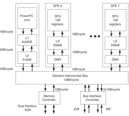
The Cell Broadband Engine Architecture (CBEA) [39] is designed to achieve high computing performance with better area/performance and power/performance ratios than the conventional multi-core architectures. The CBEA defines a het- erogeneous multi-processor architecture where general purpose processors called Power Processor Elements (PPE) and SIMD 1 processors called Synergistic Pro- cessor Elements (SPE) are connected via a high speed on-chip coherent bus called Element Interconnect Bus (EIB). The CBEA architecture is flexible and the ratio of the different elements can be defined according to the requirements of the dif- ferent applications. The first implementation of the CBEA is the Cell Broadband Engine (Cell BE or informally Cell) designed for the Sony Playstation 3 game console, and it contains 1 PPE and 8 SPEs. The block diagram of the Cell is shown in Figure 1.12.
The PPE is a conventional dual-threaded 64bit PowerPC processor which can run existing operating systems without modification and can control the operation of the SPEs. To simplify processor design and achieve higher clock speed instruction reordering is not supported by the PPE. IT has a 32kB Level 1 (L1) cache memory, which is a set-associative, parity protected, 128 bit sized cache-line memory, and 512kB Level 2 (L2) unified (data and instruction) cache memory.
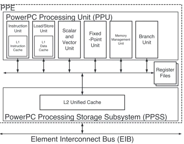
The Power Processing Element contains several functional units, which com- poses the Power Processing Unit shown in Figure 1.13.
The PPU executes the PowerPC Architecture instruction set and the Vec- tor/SIMD Multimedia Extension instructions. The Instruction Unit performs the instruction-fetch, decode, dispatch, issue, branch, and completion portions of execution. It contains the L1 instruction cache. The Load Store Unit performs all data accesses, including execution of load and store instructions. It contains the L1 data cache. The Vector/Scalar Unit includes a Floating-Point Unit (FPU) and a 128-bit Vector/SIMD Multimedia Extension Unit (VXU), which together
1SIMD - Single Instruction Multiple Data
SPU 128 registers
LS 256kB
DMA SPE 0
SPU 128 registers
LS 256kB
DMA SPE 7
Element Interconnect Bus 128B/cycle L1
2x32kB
Memory Controller L2
512kB
Bus Interface Controller PowerPC
core
16B/cycle
16B/cycle 128B/cycle 16B/cycle
32B/cycle
16B/cycle 2x16B/cycle
Dual Rambus
XDR IOIF BIF
16B/cycle
Figure 1.12: Block diagram of the Cell processor
Scalar and Vector
Unit
PPE
PowerPC Processing Unit (PPU)
Fixed -Point Unit
Memory Management
Unit
Instruction Unit
L1 Instruction
Cache
Load/Store Unit
L1 Data Cache
Branch Unit
Register Files
PowerPC Processing Storage Subsystem (PPSS)
L2 Unified Cache
Element Interconnect Bus (EIB)
Figure 1.13: Block diagram of the functional units of the PowerPC Processor Element
execute floating-point and Vector/SIMD Multimedia Extension instructions. The Fixed-point Unit executes fixed-point operations, including add, multiply, divide, compare, shift, rotate, and logical instructions. The Memory Management Unit manages address translation for all memory accesses.
The EIB is not a bus as suggested by its name but a ring network which contains 4 unidirectional rings where two rings run counter to the direction of the other two. The EIB supports full memory-coherent and symmetric multi- processor (SMP) operations. Thus, a CBE processor is designed to be ganged coherently with other CBE processors to produce a cluster. The EIB consists of four 16-byte-wide data rings. Each ring transfers 128 bytes at a time. Processor elements can drive and receive data simultaneously. The EIB ˝Os internal maxi- mum bandwidth is 96 bytes per processor-clock cycle. Multiple transfers can be in-process concurrently on each ring, including more than 100 outstanding DMA memory requests between main storage and the SPEs.
The on-chip Memory Interface Controller (MIC) provides the interface be- tween the EIB and physical memory. It supports one or two Rambus Extreme Data Rate (XDR) memory interfaces, which together support between 64 MB and 64 GB of XDR DRAM memory. Memory accesses on each interface are 1 to 8, 16, 32, 64, or 128 bytes, with coherent memory-ordering. Up to 64 reads and 64 writes can be queued. The resource-allocation token manager provides feedback about queue levels.
The dual-channel Rambus XDR memory interface provides very high 25.6GB/s memory bandwidth. The XDR DRAM memory is ECC-protected, with multi- bit error detection and optional single-bit error correction. I/O devices can be accessed via two Rambus FlexIO interfaces where one of them (the Broadband Interface (BIF)) is coherent and makes it possible to connect two Cell processors directly.
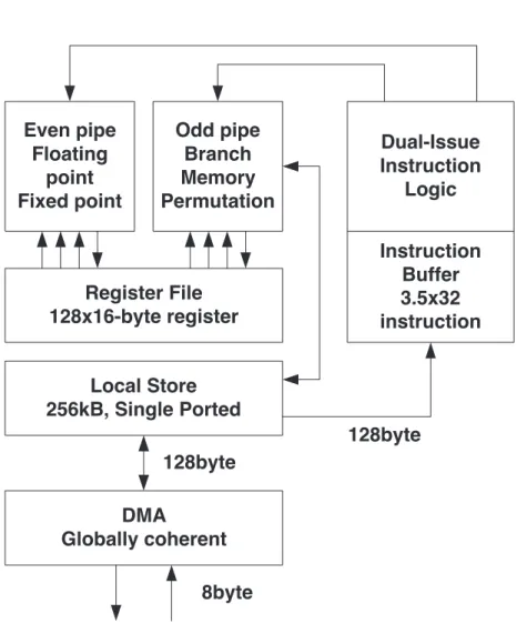
The SPEs are SIMD only processors which are designed to handle streaming data. Therefore they do not perform well in general purpose applications and cannot run operating systems. Block diagram of the SPE is shown in Figure 1.14.
The SPE has two execution pipelines: the even pipeline is used to execute floating point and integer instructions while the odd pipeline is responsible for
Register File 128x16-byte register Even pipe
Floating point Fixed point
Odd pipe Branch Memory Permutation
Local Store 256kB, Single Ported
DMA
Globally coherent
Dual-Issue Instruction
Logic
Instruction Buffer 3.5x32 instruction
128byte
128byte
8byte
Figure 1.14: Block diagram of the Synergistic Processor Element
the execution of branch, memory and permute instructions. Instructions for the even and odd pipeline can be issued in parallel. Similarly to the PPE the SPEs are also in-order processors. Data for the instructions are provided by the very large 128 element register file where each register is 16byte wide. Therefore SIMD instructions of the SPE work on 16byte-wide vectors, for example, four single precision floating point numbers or eight 16bit integers. The register file has 6 read and 2 write ports to provide data for the two pipelines. The SPEs can only address their local 256KB SRAM memory but they can access the main memory of the system by DMA instructions. The Local Store is 128byte wide for the DMA and instruction fetch unit, while the Memory unit can address data on 16byte boundaries by using a buffer register. 16byte data words arriving from the EIB are collected by the DMA engine and written to the memory in one cycle. The DMA engines can handle up to 16 concurrent DMA operations where the size of each DMA operation can be 16KB. The DMA engine is part of the globally coherent memory address space but we must note that the local store of the SPE is not coherent.
Consequently, the most significant difference between the SPE and PPE lies in how they access memory. The PPE accesses main storage (the effective-address space) with load and store instructions that move data between main storage and a private register file, the contents of which may be cached. The SPEs, in contrast, access main storage with Direct Memory Access (DMA) commands that move data and instructions between main storage and a private local memory, called a local store or local storage (LS). An SPE’s instruction-fetches and load and store instructions access its private LS rather than shared main storage, and the LS has no associated cache. This three-level organization of storage (register file, LS, main storage), with asynchronous DMA transfers between LS and main storage, is a radical break from conventional architecture and programming models, because it explicitly parallelizes computation with the transfers of data and instructions that feed computation and store the results of computation in main storage.
1.5.2 Cell Blade Systems
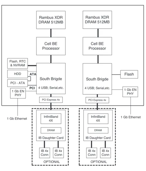
Cell blade systems are built up from two Cell processor chips interconnected with a broadband interface. They offer extreme performance to accelerate compute- intensive tasks. The IBM Blade Center QS20 (see Figure 1.15) is equipped with two Cell processor chips, Gigabit Ethernet, and 4x InfiniBand I/O capability. Its computing power is 400GFLOPS peak. Further technical details are as follows:
• Dual 3.2GHz Cell BE Processor Configuration
• 1GB XDRAM (512MB per processor)
• Blade-mounted 40GB IDE HDD
• Dual Gigabit Ethernet controllers
• Double-wide blade (uses 2 BladeCenter slots)
Several QS20 may be interconnected in a Blade Center house with max.
2.8TFLOPS peak computing power. It can be reached by utilizing maximum 7 Blades per chassis.
The second generation blade system is the IBM Blade Center QS21which is equipped with two Cell processor chips, 1GB XDRAM (512MB per proces- sor) memory, Gigabit Ethernet, and 4x InfiniBand I/O capability. Several QS21 may be interconnected in a Blade Center chassis with max. 6.4TFLOPS peak computing power. The third generation blade system is the IBM Blade Cen- ter QS22 equipped with new generation PowerXCell 8i processors manufactured using 65nm technology. Double precision performance of the SPEs are signifi- cantly improved providing extraordinary computing density up to 6.4 TFLOPS single precision and up to 3.0 TFLOPS double precision in a single Blade Center house. These blades are the main building blocks of the world’s fastest super- computer (2009) at Los Alamos National Laboratory which first break through the ”petaflop barrier” of 1,000 trillion operations per second. The main building blocks of the world’s fastest supercomputer, besides the AMD Opteron X64 cores, are the Cell processors. The Cell processors produce 95% computing power of the entire system (or regarding computational task), while the AMD processors
ATA
Rambus XDR DRAM 512MB
Rambus XDR DRAM 512MB
Cell BE Processor Cell BE
Processor
South Brigde 4 USB; Serial,etc.
Flash, RTC
& NVRAM HDD
1 Gb EN PHY PCI - ATA
PCI
PCI Express 4x
South Brigde 4 USB; Serial,etc.
PCI Express 4x
Flash
1 Gb EN PHY
1 Gb Ethernet InfiniBand 1 Gb Ethernet
4X
DRAM
IB Daughter Card
IB 4x Conn
IB 4x Conn OPTIONAL
InfiniBand 4X
DRAM
IB Daughter Card
IB 4x Conn
IB 4x Conn OPTIONAL
Figure 1.15: IBM Blade Center QS20 architecture
mounted on LS22 board are for supporting internode communication. The peak computing performance is 6.4 TFLOPS single precision and up to 3.0 TFLOPS double precision in a single Blade Center house.
1.6 Recent Trends in Many-core Architectures
There are a number of different implementations of array processors commercially available. The CSX600 accelerator chip from Clearspeed Inc. [40] contains two main processor elements, the Mono and the Poly execution units. The Mono execution unit is a conventional RISC processor responsible for program flow control and thread switching. The Poly execution unit is a 1-D array of 96 execution units, which work on a SIMD fashion. Each execution unit contains a 64bit floating point unit, integer ALU, 16bit MAC (Multiply Accumulate) unit, an I/O unit, a small register file and local SRAM memory. Although the architecture runs only on 250MHz clock frequency the computing performance of the array may reach 25GFlops.
The Mathstar FPOA (Field Programmable Object Array) architecture [41]
contains different types of 16bit execution units, called Silicon Objects, which are arranged on a 2-D grid. The connection between the Silicon Objects is pro- vided by a programmable routing architecture. The three main object types are the 16bit integer ALU, 16bit MAC and 64 word register file. Additionally, the architecture contains 19Kb on-chip SRAM memories. The Silicon objects work independently on a MIMD (Multiple Instruction Multiple Data) fashion. FPOA designs are created in a graphical design environment or by using MathStar’s Silicon Object Assembly Language.
The Tilera Tile64 architecture [42] is a regular array of general purpose pro- cessors, called Tile Processors, arranged on an 8×8 grid. Each Tile Processor is 3-way VLIW (Very Long Instruction Word) architecture and has a local L1, L2 cache and a switch for the on-chip network. The L2 cache is visible for all processors forming a large coherent shared L3 cache. The clock frequency of the architecture is in the 600-900MHz range providing 192GOps peak computing power. The processors work with 32bit data words but floating point support is not described in the datasheets.
Chapter 2
Mapping the Numerical
Simulations of Partial Differential Equations
2.1 Introduction
Performance of the general purpose computing systems is usually improved by increasing the clock frequency and adding more processor cores. However, to achieve very high operating frequency very deep pipeline is required, which cannot be utilized in every clock cycle due to data and control dependencies. If an array of processor cores is used, the memory system should handle several concurrent memory accesses, which requires large cache memory and complex control logic.
In addition, applications rarely occupy fully all of the available integer and floating point execution units.
Array processing to increase the computing power by using parallel compu- tation can be a good candidate to solve architectural problems (distribution of control signals on a chip). Huge computing power is a requirement if we want to solve complex tasks and optimize to dissipated power and area at the same time.
In this work the IBM Cell heterogeneous array processor architecture (mainly because its development system is open source), and an FPGA based implemen- tations is investigated. It is exploited here in solving complex, time consuming problems.
The main motivation of the Chapter is to find a method for implementing
35