DEVICES AND ITS APPLICATIONS Ph.D. thesis
Zolt´an Nagy
Supervisor: Professor P´eter Szolgay Information Science Ph.D. School
Department of Image Processing and Neurocomputing University of Pannonia
Veszpr´em, Hungary
2007
Ertekez´es doktori (PhD) fokozat elnyer´ese ´erdek´eben.´
´Irta: Nagy Zolt´an
K´esz¨ult a Pannon Egyetem Informatikai Tudom´anyok Doktori Iskol´aja keret´eben T´emavezet˝o: Dr. Szolgay P´eter
Elfogad´asra javaslom (igen / nem)
(al´a´ır´as) A jel¨olt a doktori szigorlaton ... % -ot ´ert el,
Az ´ertekez´est b´ır´al´ok´ent elfogad´asra javaslom:
B´ır´al´o neve: ... ... igen /nem
...
(al´a´ır´as) B´ır´al´o neve: ... ... igen /nem
...
(al´a´ır´as) A jel¨olt az ´ertekez´es nyilv´anos vit´aj´an ...% - ot ´ert el
Veszpr´em, ...
a B´ır´al´o Bizotts´ag eln¨oke A doktori (PhD) oklev´el min˝os´ıt´ese...
...
Az EDT eln¨oke
ii
I would like to give all my thanks to my parents, my grandparents and also my sister for their constant support during my studies.
I would like to thank my supervisor, Professor P´eter Szolgay, for his consistent support, help, guidance and advices during the years that led to the writing of this work.
I am very grateful to dr. Attila Katona who introduced me to the high level design of digital circuits and programmable logic devices.
I also would like to thank my colleagues at the CNN Applications Laboratory of the Department of Image Processing and Neurocomputing, University of Veszpr´em (P´eter Kozma, Zsolt V¨or¨osh´azi, P´eter Sonkoly and S´andor Kocs´ardi) for interesting and helpful discussions.
iii
Implementation of emulated digital CNN-UM architecture on programmable logic devices and its applications
Cellular Neural Network (CNN) is a locally connected two dimensional analog proces- sor array. CNN was found to be very efficient in real time image and signal processing tasks where the computation is carried out by some kind of spatio-temporal phenom- ena. The limited accuracy of the analogue VLSI CNN chips does not make it possible to use the results in engineering applications.
This dissertation demonstrates how to use programmable logic devices to imple- ment emulated digital CNN-UM architectures efficiently. By using a digital architec- ture the spatio-temporal behavior of the CNN array can be accurately computed. The computing precision of the presented architecture can be configured which makes it possible to use only the required amount of resources during the computations. Addi- tionally decreasing computing precision results in higher operating frequency therefore accuracy of the solution can be traded for computing performance.
Advantages of the new emulated digital CNN architecture is demonstrated in the solution of various Partial Differential Equations (PDE). New heuristic algorithms are introduced to determine the optimal precision for the solution and improve the efficiency of the implementation.
iv
Emul´ alt digit´ alis CNN-UM architekt´ ura megval´ os´ıt´ asa
´
ujrakonfigur´ alhat´ o ´ aramk¨ or¨ ok¨ on ´ es alkalmaz´ asai
A Cellul´aris Neur´alis H´al´ozatok (Cellular Neural Network (CNN) lok´alisan ¨ossze- k¨ot¨ott anal´og processzor t¨omb¨ok. A CNN igen hat´ekonynak bizonyult val´osidej˝u k´ep
´es jelfeldolgoz´asi feladatokban, ahol a sz´am´ıt´asokat valamilyen t´er-id˝obeli dinamika v´egzi el. Azonban a jelenlegi anal´og VLSI CNN chip-ek pontoss´aga nem elegend˝o az eredm´enyek m´ern¨oki alkalmaz´asokban t¨ort´en˝o felhaszn´al´as´ahoz.
A disszert´aci´o bemutatja hogyan lehet programozhat´o logikai eszk¨oz¨oket haszn´alni emul´alt digit´alis CNN-UM architekt´ur´ak hat´ekony megval´os´ıt´as´ara. Digit´alis ar- chitekt´ura haszn´alat´aval a CNN t¨omb t´er-id˝obeli viselked´ese pontosan kisz´am´ıthat´o.
A bemutatott architekt´ura sz´am´ıt´asi pontoss´aga konfigur´alhat´o, amely lehet˝ov´e teszi, hogy csak a sz¨uks´eges er˝oforr´asokat haszn´aljuk a sz´am´ıt´asok sor´an. Tov´abb´a a sz´am´ıt´asi pontoss´ag cs¨okkent´ese magasabb m˝uk¨od´esi frekvenci´at eredm´enyez teh´at a megold´as pontoss´ag´at sz´am´ıt´asi teljes´ıtm´enyre v´althatjuk.
A szerz˝o az ´uj emul´alt digit´alis architekt´ura el˝onyeit parci´alis differenci´al egyen- letek megold´as´an kereszt¨ul szeml´elteti. ´Uj heurisztikus elj´ar´asokat mutat be az op- tim´alis sz´am´ıt´asi pontoss´ag meghat´aroz´as´ara ´es a megval´os´ıt´as hat´ekonys´ag´anak jav´ı- t´as´ara.
v
Impentation du CNN-UM architecture num´ erique ´ emul´ e sur les dispositifs logiques programmables et son applications
Le R´eseau Cellulaire Neurale (Cellular Neural Network - CNN) est des blocs de pro- cesseurs analogues localement reli´es. CNN s’avereait tr´es efficace dans les tˆaches de processus r´eel temps image et signes o´u les calculations ont ´et´e fait par une certaine dinamique spatio-temporelle. Par contre l’exactitude des VLSI CNN puces analogues actuelles n’est pas suffisante pour l’utiliser dans les emplois d’ing´enieur.
Cette dissertation pr´esente comment les outils logiques programmables peuvent ˆetre utilis´es efficacement pour r´ealiser les CNN-UM architectures num´eriques ´emul´es.
Par l’utilisation de l’architecture num´erique le comportement spatio-temporel est pr´ecisamment calculable. L’exactitude de l’architecture pr´esent´ee peut ˆetre configur´ee qui nous donne la possibilit´e d’utiliser seulement des ressources n´ecessaires au cours des calculations. En plus la baisse de l’exactitude de la calculation amm´ene ´a un resultat de fr´equence fonctionnelle plus haut donc on peut changer l’exactitude du resultat en fonctionnement de calculation.
Les avantages de la nouvelle architecture num´erique sont pr´esent´ees par la racine des ´equitations aux d´eriv´ees partielles (EDP). Ce dissertation introduit des nouveaux algorithmes heuristiques pour determiner l’exactitude optimale de calcule et pour augmenter l’efficaciter de la r´ealisation.
vi
1 Introduction 1
1.1 Cellular Neural/Non-linear Networks . . . 3
1.1.1 CNN theory . . . 3
1.1.2 The CNN Universal Machine . . . 5
1.1.3 CNN-UM implementations . . . 6
1.2 Programmable Logic Devices . . . 8
1.2.1 Field Programmable Gate Arrays . . . 10
1.2.2 Virtex family . . . 13
1.2.3 Virtex-E and Virtex-EM family . . . 18
1.2.4 Virtex-II family . . . 18
1.2.5 Virtex-II Pro and Virtex-II ProX family . . . 20
2 Emulated Digital CNN-UM architectures 22 2.1 The CASTLE architecture . . . 23
3 The Falcon architecture 30 3.1 Nearest neighborhood sized templates on the Falcon architecture . . . 31
3.1.1 The Memory unit . . . 33
3.1.2 The Mixer unit . . . 34
3.1.3 The Arithmetic unit . . . 39
3.1.4 The Control unit . . . 42
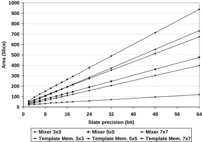
3.2 Arbitrary sized templates on the Falcon architecture . . . 45
3.2.1 The Memory unit . . . 45
3.2.2 The Mixer unit . . . 46
3.2.3 The Arithmetic unit . . . 50
3.3 The multi-layer Falcon architecture . . . 52
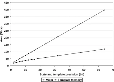
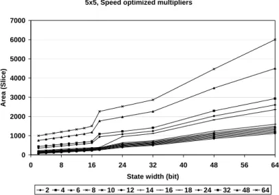
3.4 Area optimization by using distributed arithmetic . . . 55
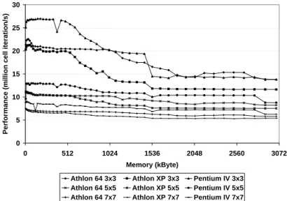
3.5 Performance comparisons . . . 60
3.6 Implementation of a real emulated digital CNN system . . . 68
3.7 Summary . . . 70
vii
4.2.1 The Heat equation . . . 80
4.2.2 The Wave equation . . . 85
4.3 Tactile sensor modeling . . . 93
4.4 Barotropic ocean model . . . 101
5 Recent advances in microprocessor and FPGA technology 113 5.1 Multiprocessors . . . 113
5.2 The Cell architecture . . . 116
5.3 New FPGA architectures . . . 119
5.3.1 Virtex-4 . . . 119
5.3.2 Virtex-5 . . . 121
5.3.3 Spartan-3, Spartan-3DSP . . . 123
5.4 Summary . . . 125
6 Conclusions 126 6.1 Theses . . . 127
6.2 The Author’s Publications . . . 131
6.3 T´ezisek magyar nyelven . . . 133
Bibliography 138 A Detailed area requirement diagramms of Chapter 3 141 B Detailed computing performance diagramms of Section 3.5 147 C Detailed results of Chapter 4 155 C.1 Simple mechanical system . . . 156
C.2 The Wave equation . . . 157
viii
Introduction
Though the scaling-down covers the problem of increasing computational needs there are some problems which are difficult to solve on traditional digital computers. Typ- ical examples are pattern recognition, data organization, clustering and solution of partial differential equations. Neural networks are proved to be more feasible for these applications than digital computers but they are not used expansively in in- dustrial applications because of the imperfections of the neural hardware. The most important drawback of a general neural network is that quick reprogramming is not possible which restricts its use in very specific applications. Additionally assuming a fully connected neural network is a major obstacle of the implementation because the complexity increases exponentially with the number of processors.
Cellular Neural Networks [1] solves this interconnection bottleneck by arranging the processing elements in a square grid and connecting each cell to its local neighbor- hood. This approach makes it possible to integrate large number of analog processors on a single chip. CNN was found to be very efficient in real time image and signal pro- cessing tasks where the computation is carried out by some kind of spatio-temporal phenomena [2]. But the limited accuracy of the current analogue VLSI CNN chips does not make it possible to solve partial differential equations accurate enough to use the results in engineering applications.
By using a digital architecture to emulate the CNN dynamics these limitations can be solved but the speed of these architectures is one order smaller than its ana- logue counterparts. Designing a full custom digital VLSI architecture is very time consuming and costly especially when small number of chips are manufactured. The development costs of an emulated digital CNN architecture can be reduced by using programmable devices during the implementation. The main advantage of the use of reconfigurable devices is that it makes the design and implementation of a digital
1
architecture without any concern about the manufacturing technology possible. Ad- ditionally technology changes become easier because only small portions of the design should be redesigned or no redesign is required at all.
This dissertation demonstrates how to use programmable logic devices to imple- ment emulated digital CNN-UM architectures efficiently. The computing precision of the presented architecture can be configured which makes it possible to use only the required amount of resources during the computations. On the current analog and digital VLSI implementations only nearest neighbor templates can be used but several applications require larger templates e.g. texture segmentation. By modifying the basic emulated digital CNN-UM architecture its capabilities can be extended to use arbitrary sized templates.
CNN can be used very efficiently in the solution of partial differential equations [3]
and complex dynamical systems [4]. But usually a multi-layer CNN structure or non- linear templates are required in these applications, which are still unsupported or have several limitations in the recent analog CNN-UM implementations. Additionally the usefulness of the analog VLSI solution is limited by its relatively low computing pre- cision. These issues can be solved by using emulated digital CNN-UM architectures because its capabilities can be extended to emulate multi-layer CNN structure or use nonlinear templates. Additionally the symmetrical nature of the various spatial dif- ference operators makes it possible to optimize the general CNN-UM architecture for each partial differential equation. Implementation of these specialized architectures requires smaller area and has higher performance. Fast and efficient implementation of these extended emulated digital architectures on today high density, high perfor- mance programmable logic devices requires high-level hardware description language.
By implementing the emulated digital architectures on reconfigurable devices makes it possible to use the same hardware environment in completely different applications.
In the first two chapters a short introduction into the fundamentals of Cellular Neural Networks and programmable logic devices are presented. In the second part of the dissertation implementation details and performance comparison of the various emulated digital CNN-UM implementations are described. In the last part application of the emulated digital CNN-UM architectures in the solution of partial differential equations is presented.
1.1 Cellular Neural/Non-linear Networks
1.1.1 CNN theory
Cellular Neural/Non-linear Network [1] contains identical analog processing elements called cells. These cells are arranged on a 2 or k-dimensional square grid. Each cell is connected to its local neighborhood via programmable weights which are called the cloning template. The CNN cell array is programmable by changing the cloning template. The local neighborhood of the cell is defined by the following equation:
Sr(ij) ={C(kl) : max{|k−i|,|l−j|} ≤r} (1.1) In the simplest case the sphere of influence is 1 thus the cell is connected to only its nearest neighbors as show in Figure 1.1. Input, output and state variables of the CNN cell array are continuous functions in time. The CNN cell dynamics can be implemented by the electronic circuit shown in Figure 1.2. The state equation of a cell can be described by the following ordinary differential equation:
Cxv˙xij(t) =− 1 Rx
vxij(t) + X
kl∈Sr(ij)
Aij,kl·vykl(t) + X
kl∈Sr(ij)
Bij,kl·vukl(t) +zij (1.2)
Figure 1.1: A two-dimensional CNN defined on a square grid with nearest neighbor connections
I Eij
vuij vxij
Cx Rx I (ij,kl)xu I (ij,kl)xy Iyx Ry
vyij
Figure 1.2: Electronic circuit model of one CNN cell
wherevxij is the state,vyij is the output andvuij is the input voltage of the cell. Aij is the feedback andBij is the feed-forward template. The state of the cells is connected to the output via a nonlinear element which is shown in Figure 1.3 and described by the following function:
yij =f(xij) = |x+ 1|+|x−1|
2 =
1 xij(t)>1 xij(t) −1≤xij(t)≤1
−1 xij(t)<−1
(1.3)
Vxij f(Vxij)
1
1
-1 -1
Figure 1.3: The output nonlinearity: unity gain sigmoid function
In most cases the Cx and Rx values are assumed to be 1 which makes it possible to simplify the state equation as follows:
˙
xij(t) =−xij(t) + X
kl∈Sr(ij)
Aij,kl·ykl(t) + X
kl∈Sr(ij)
Bij,kl·ukl(t) +zij (1.4) where x, y, u and z are the state, output, input and the cell bias value of the corre- sponding CNN cell respectively. Template matrices Aij and Bij are space invariants if its values do not depend on the (i, j) position of the cell otherwise it is called a space variant.
In order to fully specify the dynamics of a CNN cell array the boundary conditions have to be defined. In the simplest case the edge cells are connected to a constant value: this called Dirichlet or fixed boundary condition. If the cell values are du- plicated at the edges, the system does not lose energy: this is called Neumann or zero-flux boundary condition. In case of circular boundary conditions the edge cells see the values at the opposite sides thus cell array can be placed on a torus.
By stacking several CNN arrays on each other and connecting them a multi-layer CNN structure can be defined. The state equation of one layer can be described by the following equation:
˙
xm,ij(t) =−xm,ij(t) +
p
X
n=1
X
kl∈Sr(ij)
Amn,ij,kl·yn,kl(t) +
+ X
kl∈Sr(ij)
Bmn,ij,kl·un,kl(t)
+zm,ij (1.5) wherepis the number of layers, mis the actual layer andAmnand Bmn are templates which connect the output of the nth layer to the mth layer.
1.1.2 The CNN Universal Machine
VLSI implementation of the previously described CNN array has very high computing power but algorithmic programmability is required to improve its usability. The CNN Universal Machine (CNN-UM) [5] is a stored program analogic computer based on the CNN array. To ensure programmability, a global programming unit was added to the array. This new architecture is able to combine analog array operations with local logic efficiently. The base CNN cells are extended by adding local analog and logic memories to ensure an efficient reuse of intermediate results. Additionally the cell elements can be equipped with local sensors for faster input acquisition and additional circuitry makes cell-wise analog and logical operations possible.
According to the Turing-Church thesis the Turing Machine, the grammar and the µ-recursive functions are equivalent. The CNN-UM is universal in Turing sense because every µ-recursive function can be computed on this architecture.
1.1.3 CNN-UM implementations
Since the introduction of the CNN Universal Machine in 1993 several CNN-UM imple- mentations have been developed. These implementations are ranged from the simple software simulators to the analog VLSI solutions. Properties and performance of the recent CNN-UM architectures are summarized in Table 1.1.
The simplest and most flexible implementation of the CNN-UM architecture is the software simulation. Every feature of the CNN array can be configured e.g. the template size, the number of layers, space variant and nonlinear templates can be
Table 1.1: Comparison of the recent CNN-UM implementations
Pentium IV
Intel Itanium
Intel Xeon
TMS 320C6X
VIRTEX XCV300
VIRTEX XC2V6000 Clock
frequency 2GHz 1.5GHz 3.2GHz 1.2GHz 200MHz 250MHz
Feature
size 0.13µm 0.13µm 0.13µm 0.12µm 0.22µm 0.15µm
Chip area 1.27cm2 3.74cm2 N/A 1.1cm2 1.2cm2 3.5cm2
Number of physical
processing element 1 1 1 1 7 (12bits) 48 (18bits)
Cascadability no no no no yes yes
Dissipation 50W 130W 100W 1W 3W 15W
3*3 convolution 140ms 110ms 87ms 16.384ms 35ms 4.09ms
Erosion / Dilation 270ms 220ms 170ms 32.76ms 70ms 8.19ms
Laplace
(15 iterations) 2000ms 1560ms 1250ms 245.7ms 175ms 61.44ms
Accuracy control no no no no yes yes
CASTLE With pipeline
64*64 CNN-UM
128*128 CNN-UM
IBM
Blue Gennie Xenon Clock
frequency 200MHz 1/10MHz 32MHz 700MHz 100MHz
Feature
size 0.35µm 0.5µm 0.35µm 0.18µm 0.18µm
Chip area 0.68cm2 1cm2 1.45cm2 6.9468m2 0.25cm2
Number of physical
processing element 3*2 4096 16384 65536 3072
Cascadability yes yes yes no no
Dissipation <0.8W 1.3W <4W 491.52kW <0.5W
3*3 convolution 2.67ms (12 bit)
1.34ms (6 bit) 10.6ms 1.749ms 3.18ms 5-25ms
Erosion / Dilation 5.34ms (12 bit)
2.67ms (6 bit) 10.6ms 1.749ms 3.18ms 0.1ms
Laplace (15 iterations)
39.6ms (12 bit)
19.8ms (6 bit) 11.5ms 1.8975ms 3.45ms 60ms
Accuracy control yes no no no no
used etc. But flexibility is traded for performance because the software simulation is very slow even if it is accelerated by using processor specific instructions or Digital Signal Processors.
The performance can be improved by using emulated digital CNN-UM architec- tures [6] where small specialized processor cores are implemented on reconfigurable devices or by using custom VLSI technology. These architectures are 1-2 orders faster than the software simulation but slower than the analog CNN-UM implementations.
The most powerful CNN-UM implementations are the analog VLSI CNN-UM chips [7]. The recent arrays contain 128×128 elements but its accuracy is limited to 7 or 8 bits. Additionally these devices are very sensitive to temperature changes and other types of noises.
1.2 Programmable Logic Devices
The term programmable logic device (PLD) is used referring to any type of inte- grated circuit that can be configured by the end user for a special design imple- mentation [8]. If the device is programmed ”in the field” by the end user it is also called field programmable logic devices. One of the simplest and most commonly used programmable logic devices are the one time programmable read-only memories (PROM). These devices are available in two versions: mask programmable devices, which are programmed by the manufacturer, and the field programmable devices, which can be configured by the end user. These simple devices were used as look-up tables to implement arbitrary logic functions but the size of the ROM required for a given logic function grows exponentially according to the number of inputs. The next generation of programmable devices was introduced in the mid-1970’s. These devices combined the PROM architecture with a programmable logic array. The field programmable logic array (FPLA) is shown in Figure 1.4. It has fixed number of in- puts, outputs and product terms. The device can be divided into two parts the AND array and the OR array where both arrays are programmable. The FPLAs were not successful because the large number of programmable connections slowed down the device furthermore the lack of development tools makes these devices hard to use.
The introduction of the programmable array logic (PAL) in the late 1970s makes these devices widely accepted. The PAL architecture contains a programmable AND array but the OR array is fixed and each output is a sum of a specific set of product terms. New development tools were introduced at the same time, which made it pos- sible to simplify the design process. These devices were widely used as replacements of small- to medium-scale integrated ”glue-logic” circuits to provide high packaging density. Other benefits were the shorter design verification cycle and the possibility of logic upgrades in the field even when the product was released.
The main disadvantage of these simple programmable logic devices is the fixed logic allocation and the fully committed logic structure, which results in very low silicon utilization. Today high density PLDs try to solve this inefficiency problem by using more flexible logic block structure and more flexible interconnects than the routing resources. These high density PLDs can be grouped to two main categories:
complex programmable logic devices (CPLD) and field programmable gate arrays (FPGA). In general, a CPLD consists of a few logic blocks, which are similar to a simple PLD, containing inputs, a product term array, a product term allocation function, macrocells and I/O cells as shown in Figure 1.5 These logic blocks are connected via a central switching matrix. CPLDs with their wide input structures and sum-of-products architectures are ideal choices for implementing fast and complex state machines, high speed control logic and fast decode applications.
A B C D
Q0 Q1 Q2 Q3
Programmable AND array
Programmable OR array
Figure 1.4: FPLA architecture
Programmable interconnect Logic
Block Logic Block Logic Block Logic Block I/O
Logic Block Logic Block Logic Block Logic Block
I/O
Figure 1.5: CPLD architecture
In general, an FPGA architecture consists of a large amount of logic blocks but these blocks are simpler than in the case of CPLDs. The logic blocks are usually arranged on a regular grid and connected via a programmable routing architecture, which allows arbitrary interconnection between the logic blocks.
1.2.1 Field Programmable Gate Arrays
In 1985 Xilinx introduced a new programmable logic architecture called logic cell ar- ray (LCA). The new architecture consisted of an array of independent logic cells sur- rounded by a periphery of I/O cells and included a programmable routing structure, which allowed arbitrary interconnection of the logic cells. Each logic cell contained a combinatorial function generator and a flip-flop. Each I/O block could be configured as input, output or a bi-directional pin. This architecture became the basis of the following generation of field programmable gate arrays.
FPGA architectures can be classified in two different ways based on logic cell granularity and the routing architecture. FPGA logic blocks are very different in their size and implementation capabilities.
Coarse-grained FPGAs usually use look-up tables, multiplexers or wide fan-in AND-OR structures in the logic blocks. These complex logic blocks provide high degree of functionality using a relatively small number of transistors. However larger functionality is achieved at the cost of larger number of inputs, therefore more routing resources are required. On the other hand architecture optimized synthesis tools are required to achieve high logic block utilization.
Fine grained logic blocks usually contain a few transistors or a simple two-input gate. Fine-grained FPGAs can achieve high logic utilization because it is much easier to map complex logic functions into transistor or gate level building blocks. On the other hand fine-grained FPGAs require many wire segments and programmable switches and these routing resources requires a large silicon area and increases timing delays. Therefore fine-grained FPGAs are usually slower and have lower densities than coarse-grained FPGA architectures.
The routing architecture of an FPGA contains wire segments of various lengths and programmable switches to connect these segments to form the required net for the given application. The routing architecture has a great influence on the performance and routability of a FPGA device. Routability is the capability of the FPGA device to accommodate all nets of the application. If inadequate number of wire segments is used only a small portion of the device can be utilized while adding excess number of wiring segments requires large die size and result in lower silicon efficiency. The performance of an FPGA device mainly depends on the propagation delay through routing because this gives the largest portion of the total delay. Each time a net
CLB CLB CLB CLB
CLB CLB CLB CLB
CLB CLB CLB CLB
Figure 1.6: Row-based FPGA architecture
passes through a programmable switch an additional RC delay is added increasing the total delay.
FPGAs can be classified into three groups based on routing architecture: row based FPGAs, symmetrical FPGAs and cellular architecture.
The structure of a row based FPGAs, which uses a row of coarse-grained logic blocks adjacent to the routing resources called channels, is shown in Figure 1.6.
These channels contain wiring segments of various lengths and programmable switches to connect them. To achieve complete freedom for wiring configuration one pro- grammable switch is required at every crosspoint. More switches are required be- tween the adjacent crosspoint switches to allow creation of arbitrary length tracks however the large number of switches results in large RC delay increasing the total net delays. An alternative approach is to implement sufficient number of long tracks, which span the entire device. The main advantage of this structure is the identical and predictable net delay but it requires excessive chip area.
Symmetrical FPGAs are usually built of coarse-grained blocks called configurable logic block (CLB). These logic blocks are arranged on a 2 dimensional grid which is surrounded by I/O cells as shown in Figure 1.7. The routing architecture contains vertical routing channels between the columns of logic blocks and horizontal routing channels between the rows. The routing channels provide a net of programmable wires for direct connections between the adjacent logic blocks, variable length general- purpose interconnections and long lines, which span the entire width or height of the chip.
IOB IOB IOB IOB IOB IOB IOB IOB
IOB
IOB
IOB
IOB
IOB
IOB
IOB
IOB
IOB IOB IOB IOB IOB IOB IOB IOB IOB IOB IOB IOB IOB IOB IOB IOB
CLB CLB CLB CLB
CLB CLB CLB CLB
CLB CLB CLB CLB
CLB CLB CLB CLB
Figure 1.7: Symmetrical FPGA architecture
Cellular FPGA architecture usually contains a huge number of fine grained logic blocks. The organization of the logic blocks and interconnect structure is hierarchical.
At the lowest level logic blocks are grouped into zones which can be considered as a separate array with an interface between the local and global interconnect. These zones can be efficiently used to implement small functions such as complex combi- natorial logic, counters or comparators. These functions can be combined using the medium interconnect between the zones. The short range and limited loading of local connections make them very fast.
A high performance FPGA requires a programmable interconnect switch, which has low parasitic resistance and capacitance and requires a small chip area. Other important attributes of the programmable switch are the volatility, reprogrammability and process complexity. The most commonly used programming methods are the EPROM, the antifuse and SRAM based technologies. EPROM-based technologies use a floating-gate transistor as a switch element. This type of switch transistor can be turned off, by injecting charge to the floating gate. The charge can be removed from the floating gate either electrically or by illuminating it with ultra violet light.
These technologies are mainly used in CPLD devices.
Antifuse technologies use different insulator materials between two metal layers.
The antifuse switch is a two-terminal device, which has a very high resistance in unprogrammed state. On the application of a high voltage the antifuse can be blown, which creates a low resistance permanent link. The two most common types of insulator materials are the oxide-nitride-oxide (ONO) and the amorphous silicon.
The main advantage of the antifuse technology is the low parasitic capacitance and
resistance of the switches. This results in a much faster operation because net delays are determined by RC time constants. A disadvantage of the antifuse technology is that it requires additional processing steps and masks which make migration to the next process generation difficult. Another disadvantage is that programming of the antifuses requires extra on chip circuitry which is used only once to deliver the high programming voltage and current to the antifuse switches.
SRAM-based programmable devices uses static RAM cells to control pass gates or multiplexers. Since the value of memory cells does not change during normal operation, they are built for stability and density rather than speed. The main disadvantage of the SRAM-based FPGAs is their volatility because SRAM cells are erased when the power is turned off and the chip must be reprogrammed every time it is powered on. This initialization sequence requires an external nonvolatile memory to store the initial configuration of the device. Additionally large area is required to implement SRAM cells. The main advantage of the SRAM-based FPGAs is their unlimited reprogrammability. This makes in-system reconfiguration possible, which is ideal for prototype development because several configurations can be evaluated on the same board in very short time. Most of the present FPGAs can be partially reconfigured which enable arbitrary parts of the device to be reconfigured without affecting the operation of the unaltered parts.
1.2.2 Virtex family
Xilinx introduced the first member of the SRAM-based Virtex series FPGAs in 1998 [9]. The densities of the first Virtex FPGAs ranged from 50,000 to 1 million system gates. These devices were manufactured by using a 5-layer metal 0.22µm CMOS process. Family members of the Virtex FPGAs are summarized on Table 1.2.
Table 1.2: Virtex FPGA product table
Device CLB Array
Row x Col. Slices
Maximum SelectRAM
Bits
Block RAMs Block RAM Bits
Maximum Available
I/O
XCV50 16x24 384 24K 8 32K 180
XCV100 20x30 600 38K 10 40K 180
XCV150 24x36 864 54K 12 48K 260
XCV200 28x42 1,176 74K 14 56K 284
XCV300 32x48 1,536 96K 16 64K 316
XCV400 40x60 2,400 150K 20 80K 404
XCV600 48x72 3,456 216K 24 96K 512
XCV800 56x84 4,704 294K 28 112K 512
XCV1000 64x96 6,144 384K 32 128K 512
DLL I/O Blocks DLL
CLB Array
DLL I/O Blocks DLL
I/O Blocks I/O Blocks
I/O Routing
I/O Routing
I/O Routing I/O RoutingBlock RAMs Block RAMs
Figure 1.8: Virtex architecture overview
The major configurable elements of the Virtex FPGAs are the configurable logic blocks (CLB) and the I/O blocks (IOB). The structure of the device is shown in Figure 1.8. The CLBs are arranged on a grid surrounded by the IOBs. CLBs are connected via a general routing matrix (GRM), which contains an array of routing switches at the intersections of horizontal and vertical routing channels. The CLBs and the IOBs are connected via specialized routing resources around the periphery of the device to improve I/O routability. Beside these blocks the Virtex architecture also contains the following specialized elements: dedicated configurable block memories (BRAM) of 4kbits capacity, delay locked loops (DLL) for clock management and 3-state buffers for on-chip buses.
The IOBs of the Virtex architecture support 16 high performance I/O standards such as LVTTL, PCI, AGP, HSTL and SSTL. Each IOB contains 3 storage elements, an input buffer and a 3-state output buffer. The structure of the IOB is shown in Figure 1.9. The input, output and 3-state control signals can be routed directly from the inner logic or through the storage elements. Some I/O standards require reference voltages. These signals are connected externally to device pins, which serves groups of IOBs, called banks. The user I/O pins on the device are grouped into eight banks and two banks are located on every edge of the FPGA.
The basic building block of a Virtex CLB is the logic cell (LC) shown in Fig- ure 1.10. Each LC contains a 4-input function generator, a storage element and a carry generator. The Virtex CLB is built form 4 LCs organized in two slices. The
D Q
CE
Programmable delay
SR D Q CE
SR
CLK SR ICE
D Q CE
SR T
TCE
O OCE
I IQ
PAD
VREF
Weak keeper
Figure 1.9: Virtex Input / Output Block (IOB)
function generator of the logic cell is implemented as a 4-input look-up table (LUT).
In addition to operating as function generator each LUT can be configured as 16×1 bit synchronous RAM and the LUTs within a slice can be combined to form 16×2, 32×1 synchronous or 16×1 bit dual ported RAM. The LUTs also can be configured as a 16-bit shift register, which can be very efficient in deeply pipelined architectures.
To improve arithmetic performance dedicated carry logic and a XOR gate are in- cluded in every LC. This makes it possible to implement a 1 bit full adder in one LC.
Each CLB supports 2 separate carry chains and a dedicated carry path is provided between the CLB rows to further improve performance. To improve multiplier effi- ciency a dedicated AND gate is also included. Each slice contains an F5 multiplexer to combine the outputs of the LUTs in the slice. This makes it possible to implement any 5 input logic function or a 4:1 multiplexer in one slice. For similar considerations each CLB contains an additional F6 multiplexer to make implementation of any 6 input logic function or an 8:1 multiplexer in one CLB possible.
The Virtex FPGAs has hierarchical memory system along with the RAM resources in the CLBs, dedicated on-chip memory elements (BRAM) are also implemented.
Each memory element is a synchronous dual-ported 4kbit RAM with independent control signals and independently configurable data widths. The BRAMs are located in two columns on each vertical edge of the device.
The local routing resources on the Virtex FPGA provides connections between the LUTs and flip-flops of the CLB and the GRM, internal connections between the elements of one CLB and direct paths between the horizontally adjacent CLBs to eliminate the delay of a GRM as shown in Figure 1.11. The major part of the routing hierarchy is the general purpose routing which contains horizontal and vertical routing
Carry &
Control
Carry &
Control F1
F2F3 F4
LUT G1
G2 G3 G4
LUT
BY
BX
D Q
CIN COUT
SLICE 1 D Q
YB Y YQ
XB X XQ
Carry &
Control
Carry &
Control F1
F2F3 F4
LUT G1
G2 G3 G4
LUT
BY
BX
D Q
CIN COUT
SLICE 0 D Q
YB Y YQ
XB X XQ
Figure 1.10: 2-Slice Virtex CLB
channels. At each crossing of these routing channels a GRM is placed, which is a switch matrix connecting the horizontal and vertical routing resources and makes it possible for one CLB to access these resources. Each GRM is connected to its neighbors with 24 single-length lines in all four directions. Along with the single- length lines the GRM is connected to other GRMs 6 blocks away via 72 hex-lines in all four directions. These hex-lines are organized on a staggered pattern and can be driven only at their endpoints but can be accessed either at the endpoints or the midpoints. 12 horizontal and vertical long-lines, which span the full width and height of the device, can be used to distribute signals across the device quickly and efficiently. I/O routing resources are surrounded at the periphery of the CLB array and make efficient I/O signal routing between the CLB array and the IOBs possible.
Dedicated routing resources are provided to maximize performance such as horizontal routing resources for on chip 3-state buses and the dedicated carry propagation nets between the rows of CLBs. The global routing resources distribute clocks and other high fan-out signals throughout the entire device. Four global clock nets are provided for distribution of clock signals with minimal skew and each net can drive all CLB, IOB and BRAM clock pins. Other high fan-out signals can be routed through the secondary clock network, which consists of 12 backbone lines across the top and the bottom of the chip. These backbone lines can be connected to the 12 vertical long- lines at each column. The secondary clock network is more flexible than the primary because it is not restricted to routing of the clock signals.
For clock management purposes 4 fully digital delay-locked loops (DLL) are im- plemented on each Virtex FPGA. These DLLs can eliminate the skew between the input clock and the internal clock input pins throughout the device. In addition to clock de-skew, the DLLs provide phase shifting of the source clock in 90◦ increments and can double or divide the clock by various values between 1.5 to 16.
Direct connection CLB to adjacent CLBs
GRM
To adjacent GRM To adjacent
GRM
To adjacent GRM
To adjacent GRM
Direct connection to adjacent CLBs
Figure 1.11: Virtex Local Routing
GRM CLB GRM CLB GRM CLB
GRM CLB
GRM GRM GRM GRM GRM GRM GRM
Long-lines
Hex-lines
GRM GRM
GRM
GRM GRM
Direct connections
Figure 1.12: Hierarchical Routing Resources
1.2.3 Virtex-E and Virtex-EM family
The first member of the Virtex-E series FPGAs was introduced in 1999. These devices are manufactured by using a 6 metal layer 0.18µm CMOS technology. The improved manufacturing technology increased the speed and reduced the die area and the power consumption of the devices. The Virtex-E series FPGAs are offered in densities from 58,000 to 4 million system gates. Beyond the better processing technology some features of the Virtex-E FPGAs are improved. The number of supported I/O standards is increased by adding support for differential and double data rate (DDR) signaling. The clock management capabilities of the devices are also improved by the addition of four further DLLs. The memory system was also expanded, by doubling the number of dedicated block memories.
The two members of the Virtex-EM family were introduced in 2000. These devices are specialized for designs with high bandwidth and large memory requirements. The only difference between the Virtex-E and the Virtex-EM devices is the increased number of block RAM memories.
Family members of the Virtex-E and Virtex-EM FPGAs are summarized on Ta- ble 1.3.
1.2.4 Virtex-II family
The new Virtex-II series FPGAs were introduced in 2000. In addition to the im- proved manufacturing technology (8 metal layer, 0.15µm CMOS) these devices have some significant architectural improvements. These improvements include additional I/O capability by supporting more I/O standards and on-chip signal termination,
Table 1.3: Virtex-E/EM FPGA product table
Device CLB Array
Row x Col. Slices
Maximum SelectRAM
Bits
Block RAMs Block RAM Bits
Maximum Available
I/O
XCV50E 16 x 24 384 24K 16 64K 176
XCV100E 20 x 30 600 38K 20 80K 196
XCV200E 28 x 42 1,176 74K 28 112K 284
XCV300E 32 x 48 1,536 96K 32 128K 316
XCV400E 40 x 60 2,400 150K 40 160K 404
XCV600E 48 x 72 3,456 216K 72 288K 512
XCV1000E 64 x 96 6,144 384K 96 384K 660
XCV1600E 72 x 108 7,776 486K 144 576K 724
XCV2000E 80 x 120 9,600 600K 160 640K 804
XCV2600E 92 x 138 12,696 794K 184 736K 804
XCV3200E 104 x 156 16,224 1014K 208 832K 804
XCV405E 40 x 60 2,400 150K 140 560K 404
XCV812E 56 x 84 4,704 294K 280 1120K 556
Table 1.4: Virtex-II FPGA product table
Device CLB Array
Row x Col. Slices
SelectRAM 18Kbit Blocks
18x18Bit Multiplier
Blocks
DCMs
Maximum Available
I/O
XC2V40 8 x 8 256 4 4 4 88
XC2V80 16 x 8 512 8 8 4 120
XC2V250 24 x 16 1,536 24 24 8 200
XC2V500 32 x 24 3,072 32 32 8 264
XC2V1000 40 x 32 5,120 40 40 8 432
XC2V1500 48 x 40 7,680 48 48 8 528
XC2V2000 56 x 48 10,752 56 56 8 624
XC2V3000 64 x 56 14,336 96 96 12 720
XC2V4000 80 x 72 23,040 120 120 12 912
XC2V6000 96 x 88 33,792 144 144 12 1,104
XC2V8000 112 x 104 46,592 168 168 12 1,108
additional memory capacity by using larger 18kbit embedded block memories, addi- tional routing resources and embedded 18 bit by 18 bit signed multiplier blocks. The densities of these devices are ranged from 40,000 to 8 million system gates. Family members of the Virtex-II FPGAs are summarized on Table 1.4.
For native double data rate support 3 extra registers and a DDR multiplexer are added to each IOB as shown in Figure 1.13. The digitally controlled impedance (DCI) is a new feature, which provides controlled impedance and on-chip termination. This eliminates the need for external resistors and improves signal integrity on high-speed board connections.
The Virtex-II CLB contains 8 logic cells organized in 4 slices. The base structure of the slices did not change, each slice contains two 4 input LUT, two registers and carry logic. The enlarged CLB contains additional MUXFX multiplexers for improved
PAD Reg
OCK2
DDR MUX 3-state
Output
Input Reg
OCK1
Reg ICK2 Reg ICK1
Reg OCK2
Reg OCK1
DDR MUX
Figure 1.13: Virtex-II IOB Block
wide multiplexer support. This makes it possible to implement a 16:1 multiplexer in one CLB and a 32:1 multiplexer by using two CLBs. Additional dedicated routing resources inside the CLB can be used to connect the LUTs in shift register mode.
This feature allows the creation of 128-bit shift register with addressable access in one CLB.
The on-chip memory capacity of the Virtex-II FPGAs is significantly improved compared to the previous families by using 18kbit block RAMs. The block RAMs are organized in columns and distributed between the columns of CLBs.
To accelerate multiplication and save logic resources Virtex-II FPGAs have 18 bit by 18 bit embedded 2’s complement signed multipliers. These multipliers are opti- mized for high-speed operation and have a lower power consumption compared to an 18 bit by 18 bit multiplier which is implemented in slices. The large number of embedded multipliers is very rewarding in multiplication intensive DSP applications.
The clock management capabilities of the Virtex-II FPGAs are significantly im- proved. Along with the features of the previous generations Virtex-II digital clock managers (DCM) have frequency synthesis and phase shifting modes. In frequency synthesis mode the input clock can be multiplied by an arbitrary value which is de- termined by the ratio of two integers. In phase shifting mode the phase shift between the rising edge of the input and output clock of the DCM can be specified by the fraction of the input clock period or it can be dynamically adjusted.
The local and global routing resources of the Virtex-II architecture are optimized for speed and timing predictability. Each configurable block is connected to an iden- tical switch matrix to access global routing resources as shown in Figure 1.14. Switch matrices with various types of attached logic blocks are arranged on an array. The routing hierarchy of the Virtex-II architecture contains 5 levels of different types of interconnections. These are longlines, hex-lines, double lines, direct lines and fast connects. These interconnection types are similar to the previous generations but the number of lines is significantly increased and a new type of interconnection, the double line, is introduced. Double lines connect every second switch matrix and are organized in a staggered pattern. These lines can be driven only at their endpoints but can be accessed either at the endpoint or at the midpoint.
1.2.5 Virtex-II Pro and Virtex-II ProX family
The Virtex-II Pro devices were introduced in 2002. These devices are manufactured by using a 9 metal layer 0.13µm technology. The structure of the configurable blocks and the interconnections are not changed. However, hard IP blocks are added to the architecture. These are embedded PowerPC processors and high-speed serial transceivers. The embedded PowerPC processors make it possible to use these devices in Field Programmable System on Chip (FPSoC) applications more efficiently. The
18kbit Block RAM 18bit x 18bit Multiplier Switch matrix
Switch matrix
Switch matrix
Switch matrix CLB Switch
matrix IOB Switch
matrix IOB Switch
matrix IOB Switch matrix DCM
Switch matrix Switch CLB
matrix
Switch CLB matrix Switch CLB
matrix
Switch CLB matrix Switch CLB
matrix
Switch CLB matrix Switch CLB
matrix Switch
matrix IOB
Switch matrix IOB
Switch matrix IOB
Switch matrix IOB
Figure 1.14: Routing architecture of the Virtex-II FPGAs
RocketIO serial transceivers make it possible to connect these FPGAs directly to various serial connection standards such as Serial ATA or PCI-Express devices. On the other hand the number of embedded memory and multiplier cores is significantly increased. On the largest member of the family up to 556 memory and multiplier blocks can be used.
The two members of the Virtex-II ProX family were introduced in 2003. These de- vices are specialized for designs with high bandwidth requirements. The performance of the RocketIO serial transceivers is increased to 10Gb/s.
Family members of the Virtex-II Pro and Virtex-II ProX FPGAs are summarized on Table 1.5.
Table 1.5: Virtex-II Pro/ProX FPGA product table
Device Slices
BlockRAM 18Kbit Blocks
18x18Bit Multiplier
Blocks
RocketIO Transceiver
Blocks
PowerPC Processor Blocks
DCMs
Max.
User I/O
XC2VP2 1,408 12 12 4 0 4 204
XC2VP4 3,008 28 28 4 1 4 348
XC2VP7 4,928 44 44 8 1 4 396
XC2VP20 9,280 88 88 8 2 8 564
XC2VP30 13,696 136 136 8 2 8 644
XC2VP40 19,392 192 192 0, 8, or 12 2 8 804
XC2VP50 23,616 232 232 0 or 16 2 8 852
XC2VP70 33,088 328 328 16 or 20 2 8 996
XC2VP100 44,096 444 444 0 or 20 2 12 1,164
XC2VP125 55,616 556 556 0, 20, or 24 4 12 1,200
XC2VPX20 9,792 88 88 8 1 8 552
XC2VPX70 33,088 308 308 20 2 8 992
Emulated Digital CNN-UM architectures
Implementation difficulties and unreliable operation of the first analog VLSI CNN chips, especially during gray-scale image processing applications, and the inadequate performance of the software CNN simulators were the main motivation of the de- velopment of digital CNN accelerators. The main purpose of these emulators are to provide reliable gray-scale image processing capability at speeds comparable to the analog VLSI implementations.
The roots of the emulated digital CNN-UM architectures are based on the CNN hardware accelerator board (CNN-HAB) which used multiple Digital Signal Pro- cessors (DSP) to accelerate the computation of the CNN dynamics [10]. The high performance of the multiple DSP accelerator cards encouraged the designers to de- sign custom digital VLSI chips which specialized to solve the state equation of the CNN cell array. This specialization greatly reduced the area requirements of the processor and makes it possible to implement multiple processing elements on the same die. Emulated digital architectures can also benefit from scaling down by us- ing new manufacturing technologies to implement smaller and faster circuits with reduced dissipation. The first emulated digital CNN-UM processor called CASTLE was developed in SZTAKI between 1998 and 2001 [6].
The performance of the CASTLE processor array is very significant; in some cases it can be compared to the analog VLSI implementations. But the performance is increased at the expense of the flexibility because several parameters, for example:
the cell array size, the number of layers and the computing accuracy etc. must be fixed at design time.
Before the detailed discussion of the diverse Falcon configurable emulated digital CNN-UM implementations the CASTLE architecture will be introduced because some fundamental features of the Falcon architecture are based on this architecture.
22
2.1 The CASTLE architecture
The CASTLE architecture was designed to solve the state equation of the Chua-Yang model of a CNN cell:
˙
xij(t) =−xij(t) + X
kl∈Sr(ij)
Aij,kl·ykl(t) + X
kl∈Sr(ij)
Bij,kl·ukl(t) +zij (2.1) On the edges of the cell array zero-flux boundary conditions are used hence the state values on the edges should be doubled.
These state equations (2.1) can be solved by forward Euler discretization:
xij(n+ 1) = (1−h)xij(n) +h
X
kl∈Sr(ij)
Aij,kl·ykl(n)+
+ X
kl∈Sr(ij)
Bij,kl·ukl(n) +zij
(2.2) To make implementation simpler and to decrease the area of the processor the state equation should be simplified by eliminating as much computation as possible.
The state values can be bounded in the [-1,+1] range by using the full signal range model (FSR). In this model the state value of the cell is equal to the output value.
The computation can be further simplified by inserting the timestep value to the template matrices.
A′ =
ha−1,−1 ha−1,0 ha−1,1
ha0,−1 1−h+ha0,0 ha0,1
ha1,−1 ha1,0 ha1,1
B′ =
hb−1,−1 hb−1,0 hb−1,1
hb0,−1 hb0,0 hb0,1
hb1,−1 hb1,0 hb1,1
(2.3) After these simplifications the state equation can be broken into the following two parts:
xij(n+ 1) = X
kl∈Sr(ij)
A′ij,kl·xkl(n) +gij (2.4a)
gij = X
kl∈Sr(ij)
Bij,kl′ ·ukl(n) +zij (2.4b)
If the input is constant or changing slowly,gij can be treated as a constant and should be computed only once at the beginning of the computation.
The CASTLE architecture was specialized to solve equation (2.4a) and (2.4b).
Several CASTLE processor cores can be connected in an array to improve perfor- mance as shown in Figure 2.1. In this case the image is partitioned between the
CASTLE CASTLE CASTLE
CASTLE CASTLE CASTLE
CASTLE CASTLE CASTLE
Global control unit
Figure 2.1: The CASTLE array
Figure 2.2: The belt stored from the image
columns of processors. Each line of processors do one iteration and sends the results to the processors one line below. The processors can communicate via dedicated lines between the columns. The operation of the processors is controlled by the global con- trol unit. The processors require a non-overlapping two-phase clock (ph1 and ph2) for synchronization.
To solve equation (2.4a), in the nearest neighbor case, 9 state, 9 template and 1 constant values should be loaded. The large number of input parameters does not allow us to provide them from external memory in real time. On the other hand the whole image can not be stored on the chip because huge area is required to implement such a large memory. The small number of templates makes it possible to store them on chip but still 10 values should be loaded for each cell. The solution of this problem is to store a 3-pixel height belt from the image on the chip as shown in Figure 2.2.
This solution reduces the I/O requirements of the processor to load one state, one constant and one template select values and to save the computed cell value. The values stored in the belt are required in the computation of the cells in the subsequent two lines. The currently processed cell and its neighborhood can be represented by a window of 3×3 elements which is continuously moving right.