Nanotechnology
PAPER • OPEN ACCESS
Grid-type transparent conductive thin films of carbon nanotubes as capacitive touch sensors
To cite this article: Ronja Valasma et al 2020 Nanotechnology 31 305303
View the article online for updates and enhancements.
This content was downloaded from IP address 160.114.20.223 on 15/06/2020 at 07:36
Nanotechnology31(2020) 305303 (7pp) https://doi.org/10.1088/1361-6528/ab8590
Grid-type transparent conductive thin films of carbon nanotubes as capacitive touch sensors
Ronja Valasma1, Eva Bozo1, Olli Pitk¨anen1, Topias J¨arvinen1, Aron Dombovari1, Melinda Mohl1, Gabriela Simone Lorite1, Janos Kiss2,3, Zoltan Konya2,3
and Krisztian Kordas1
1Microelectronics Research Unit, Faculty of Information Technology and Electrical Engineering, University of Oulu, PO Box 4500, FI-90014 University of Oulu, Finland
2Department of Applied and Environmental Chemistry, University of Szeged, Rerrich B. t´er 1, Szeged 6720, Hungary
3MTA-SZTE Reaction Kinetics and Surface Chemistry Research Group, University of Szeged, Rerrich B. t´er 1, Szeged 6720, Hungary
E-mail:krisztian.kordas@oulu.fi
Received 4 December 2019, revised 17 January 2020 Accepted for publication 31 March 2020
Published 11 May 2020 Abstract
Transparent conductive films are used in a wide variety of devices. While solar cell top
electrodes as well as tablet and mobile phone screens require high optical transparency and low sheet resistance (>80% and <10Ω/□) to maximize power efficiency; other, less demanding applications, such as those in capacitive touch panels and antistatic coatings, in which only small currents are involved, can be managed with coatings of moderate conductivity. In this paper, we show that area-selective argon plasma treated polyethylene terephthalate surfaces are suitable for localized deposition of carbon nanotubes from their aqueous dispersions by a simple dip coating and subsequent drying processes. The as-deposited carbon nanotubes form
entangled networks in microscopic patterns over the plasma-treated surface areas with sheet resistance of <1 kΩ/□and optical transparency of ~75%. Based on this process, we demonstrate grid-type transparent conductive thin films of carbon nanotubes as capacitive touch sensors.
Since each process step is robust, easy to up and downscale, and may be implemented even in roll-to-roll and sheet-to-sheet fabrication, the demonstrated technology is promising to produce grid-type structures even at an industrial scale in the future.
Supplementary material for this article is availableonline
Keywords: transparent conductive films, plasma treatment, PET, CNTs, grid-type structures, percolation
(Some figures may appear in colour only in the online journal)
Original content from this work may be used under the terms of theCreative Commons Attribution 4.0 licence. Any further distribution of this work must maintain attribution to the author(s) and the title of the work, journal citation and DOI.
Nanotechnology31(2020) 305303 R Valasmaet al
1. Introduction
Transparent conductive metal oxides (mainly indium-doped tin oxide, ITO but also fluorine-doped tin oxide, FTO and aluminum-doped zinc oxide, AZO), with their excellent optical and electrical properties have been the benchmark for many applications for decades [1]. However, the mech- anical brittleness, increasing price and prognosis of indium becoming potentially scarce (without proper recycling if the current pace of its usage continues) have pushed industry to seek alternatives to these materials, bringing several chal- lengers to the scene [2]. Among these materials, conduct- ive polymers [3], carbon nanotubes (CNTs) [4,5], graphene [6], metal nanowires [7] and their composites [8, 9] have been the most prominent ones to brake the hegemony of inor- ganic oxide based transparent conductive films. Polymers such as poly(pyrrole)s, polyanilines and poly(thiophene)s have the advantages of mechanical flexibility and easy application on surfaces, e.g. by spin coating and printing methods (in con- trast to sputtered or combined spin-coat and thermal annealed gels of ITO and AZO) but they suffer from limited thermal and chemical stabilities as well as from moderate electrical con- ductivity. Metal nanowires have high electrical conductivity but their networks rearrange upon mechanical deformation of the substrate, which may cause reliability problems. In addi- tion, unless noble metals are applied, metal oxides develop on their surface in ambient conditions (such as Cu2O and CuO on Cu) [10,11], limiting the metal selection to expensive Au or Ag [12,13]. Difficulties related to oxidation and consequent formation of tunneling barriers between the nanowires in the network can be circumvented by passivating/protecting the surface of nanowires [14,15].
Another approach is an application of micropatterned thin films, which develop oxides on their surface, but due to the continuity of the metal film in the micropattern, the oxide layer is limited to the uppermost few atomic layers and thus does not introduce tunneling barriers for the electrical trans- port along the pattern [16]. Nanostructured carbon based thin films on the other hand are not only affordable and flexible but also show long term reliable operation even under high tem- perature operation or prolonged solar irradiation. These net- works of flexible CNTs or graphene are usually deposited from their dispersions by printing [17,18], dip coating or spraying after functionalizing and suspending them in water or organic solvents (e.g. DMF, DMSO, NMP) [19,20] but can be col- lected from the aerosol of the growth product in vertical CVD furnaces and transferred to the substrate afterwards by dry- printing [21].
Direct deposition of nanomaterials from their dispersions on polymer or other hydrophobic surfaces is rather dif- ficult from aqueous (or any other polar) dispersions. To increase the wettability of the substrates with the polar solu- tions/dispersions, one shall pre-treat the surface by either wet etching in oxidizing acids [22], or by applying plasmas [23, 24]. Polymers with ester or amide linkages may be hydro- lyzed also in alkaline media thus offering additional routes to modify their surfaces [25–27]. Such treatments introduce polar functional groups to the surface, fragment the polymer
chains, etch the topmost layers of the substrate, and/or increase the roughness of the topology making it more hydrophilic.
Since hydrophilic surface micropatterns promote pinning of the perimeter of drying droplets [28,29], after depositing dis- persions on the surface, we can avoid the stick-slip mech- anism thus control drying and consequent formation of thin films of the solid solute. Using the plasma treatment step (oxygen-argon or oxygen-nitrogen) before spraying or dip coating with CNT dispersions has been found efficient in pre- paring TCFs of continuous but random nanotube networks with sheet resistance of ~1 kΩ/□at transmittance (T) of ~90%
[30]. Furthermore, when the plasma treatment is combined with additional surface functionalization, the sheet resistance can be decreased with an order of magnitude (~130Ω/□at T ~ 90%) [31]. It is worth mentioning here, that post-treatment of the deposited CNTs in oxidizing acids can also enhance the conductivity of the tangled networks due to doping effects [32].
Here, we combine two of the aforementioned approaches to produce TCFs on polyethylene terephthalate (PET) substrates, by which we take advantage of the superb electrical properties of CNTs and the optical transparency of grid-type microstruc- tures [33]. We show that using simple and easy to scale pro- cess steps, flexible TCFs with reasonable electrical and excel- lent optical behavior are enabled, and we demonstrate that the as-obtained films are suitable for capacitive touch screen applications.
2. Materials and methods
2.1. Carbon nanotube dispersions
To form dispersions of carbon nanotubes in water without using any surfactant, we use carboxyl-functionalized single- wall CNTs (SWCNT-COOH, Sigma Aldrich #662 490) whose functional side groups can stabilize the nanomaterials in water through hydrogen bridges as well as via solvation after depro- tonation of the carboxylic acid. We used two types of disper- sions, one with higher and another with lower concentration of nanotubes. The higher concentration dispersion was prepared by adding 30.36 mg of SWCNT-COOH in distilled water of 36 ml, and stirred on a magnetic plate while adding 1 ml of (concentrated) NH4OH solution to help deprotonation of the carboxylic acid side groups thus further aiding the dispersion and stabilization of nanotubes. After stirring for 30 min, the dispersion was sonicated for 1.5 h and left to sediment for three days after which the upper supernatant fraction was col- lected. The concentration of this fraction was measured to be 0.68±0.17 mg ml−1. Stable aqueous suspensions of SWCNT- COOH but with a lower concentration were made using the same types of nanotubes as before but using a slightly differ- ent dispersion protocol. Accordingly, 10.8 mg of the SWCNT- COOH was sonicated for 3 h in a solution of 300 ml of distilled water and 3 ml of NH4OH, then the dispersion was centrifuged for 30 min at 3000 rpm and the supernatant was collected. The concentration of the obtained dispersion was measured to be 0.020±0.003 mg ml−1.
2
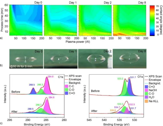
Figure 1. (a) Contact angle between the argon plasma treated PET surface and water as a function of plasma power, process time and period after the treatment. (b) Photographs of water droplets cast on a plasma treated PET (50 W for 5 min) showing a gradual decrease of hydrophobic behavior of the surface within the subsequent period of 8 d. (c) Resolved x-ray photoelectron spectra of C1 s and O1 s peaks before and after Ar plasma treatment of PET at 200 W for 30 min.
2.2. Shadow mask fabrication
A pulsed laser (LPKF ProtoLaser U3, wavelength of 355 nm, focal spot diameter of ~20µm, repetition rate of 40 kHz at an average power of 6 W, 2 outlines and 200 scans) was used to cut through polycrystalline alumina wafers (thickness of 250µm) thus producing micropatterned shadow masks for the plasma processing. The shadow mask patterns comprised par- allel lines having width of ~70µm and center to center spacing of 200µm (1×1 cm2square pattern) or 1 mm (2.5×2.5 cm2 square pattern).
2.3. Argon plasma treatment of the PET surfaces and dip coating in SWCNT-COOH dispersions
The polymer sheets (PET, Melinex ST505) were cleaned with isopropyl alcohol and dried before the actual argon plasma process. For this latter, we used an Oxford Instruments Plas- malab 80 Plus instrument with Ar gas feed at a pressure of 20 mTorr and flow rate of 20 sccm. The plasma power and process time were varied from 10 to 200 W and from 2 to 60 min, respectively. The optimum process paramet- ers for obtaining the smallest contact angles with water were found to be 200 W and 30 min, thus before the dip coating experiments each sample has been plasma treated accordingly through the shadow mask. Grid-type plasma-treated patterns were obtained by repeating the process but placing the shadow
mask over the pattern rotated at 90◦. After the plasma treat- ment, the samples were submerged manually in the aqueous SWNCT-COOH dispersions and then slowly drawn out. The films were then dried in a box furnace at ~40◦C for 5 min, and the coating process was repeated up to 20 times.
2.4. Sample characterization
X-ray photoelectron spectroscopy (XPS, Thermo Fisher Sci- entific Escalab 250 XI system with Al Kαsource of 1486.6 eV photon energy, Avantage software) was used to assess the surface composition of samples before and after plasma treatment. For the electrical measurements of the deposited SWCNT-COOH micropatterns, thin Pt electrodes were depos- ited on the edges of the samples. Sheet resistance and con- ductance values were determined from current-voltage slopes measured using a Keithley 2636A sourcemeter. Scanning elec- tron microscopy (Zeiss ULTRA plus FESEM) and atomic force microscopy (MultiMode 8, Bruker) were used to assess surface microstructure and topology, respectively. In addition, optical transmission measurements were carried out using an UV–vis-NIR Varian Cary 500 spectrophotometer.
3. Results and discussion
To find the most feasible wetting properties of the surface with the aqueous dispersion of carbon nanotubes, we optimized the
Nanotechnology31(2020) 305303 R Valasmaet al
Figure 2. SEM images of the line patterns on PET deposited using the SWCNT-COOH dispersion of lower concentration
(0.020±0.003 mg ml−1) with 5 coating (dipping) cycles. (a) Low magnification image of the surface, and a (b) higher magnification micrograph of a part between the lines not exposed previously to the argon plasma (shadowed region) showing no traces of carbon nanotubes. (c) Low magnification image of a line pattern, whose edge is magnified in panel (d). The center part is magnified in panels (e) and (f). Both center area (1) and the lanes on its sides (2) are partly covered by CNTs. Region (3) is not exposed to plasma and is similar to that displayed in panel (b). The parallel lanes in region (2) are due to plasma under-spraying caused by the imperfect lapping of the shadow mask on the surface.
plasma parameters such as power and process duration first.
The contact angle of the pristine PET surface is ~62◦ which is decreased significantly even after very short and low power Ar plasma treatment (e.g. to ~33◦ at 30 W for 2 min); how- ever, the lowest contact angles of ~10◦were obtained at high plasma powers and prolonged process times (e.g. 200 W for 30 or 60 min). As plasma processed polymer surfaces are known to relax and gradually loose the effect of the treatment [34,35], we also analyzed the time window available for subsequent wet deposition of the nanotubes from the dispersions. The relaxation was significant after 8 d in particular for the surfaces that have undergone only short plasma treatments (regardless of plasma power). On the other hand, the surfaces subjected to longer treatment could recover only partly retaining relatively low contact angles for several days (figures1(a) and (b)).
To assess the underlying cause of the decreased contact angle of water on plasma treated PET, we analyze the surface chemistry before and after plasma processing by x-ray pho- toelectron spectroscopy (figure 1(c)). In both resolved C1 s and O1 s spectra, we observe a decreased peak intensity for the C = O bond after the Ar plasma treatment, while the intensity of the C-O bond is left fairly unchanged suggesting a decomposition of the ester bond in the polymer resulting
Figure 3. (a) Logarithmic plot of film conductance (G) versus dip-coating cycle (n) with a preset conductance threshold of 0.01µS for low density CNT networks deposited from the lower
concentration CNT dispersion (0.020±0.003 mg ml−1). Inset shows the complete set of experimental data in a linear plot. (b) Logarithmic plot ofGvs.nfor patterns obtained by dip-coating the substrates in the more concentrated CNT dispersion
(0.68±0.17 mg ml−1).
in the formation of ether linkages (R-O-R) and alcohols (R-OH) of different kind. We also find emerging peaks for NaOH and water because of impurities in the plasma chamber and adsorbed moisture from the environment before loading the specimen in the XPS instrument, respectively. All these changes in the composition (in particular the alcohol termina- tions) have influence on the surface dipoles giving a plausible explanation of the improved hydrophilic behavior [36–38].
Based on the plasma treatment results, for further experi- ments, we selected plasma parameters of 200 W for 30 min to have the lowest initial contact angle (~9◦) and proceeded with the dipping step within 24 h of the treatment to avoid any significant loss of the hydrophilic behavior. To have selec- ted area plasma treatment of the surfaces (both parallel line
4
Figure 4. Optical transmittance spectra of the PET substrate before and after Ar plasma etching (parallel stripe pattern), and dip coating in the CNT dispersion (0.68±0.17 mg ml−1). Inset shows a camera image of a flexible transparent conductive film (T ~ 75% @ 550 nm and R ~ 0.7 kΩ/□).
and grid-type patterns) we applied a thin shadow mask on the polymer sheets during the plasma process. After dip coating the plasma-treated surfaces in aqueous dispersions of single- wall carbon nanotubes, the samples were dried, and the pro- cess was repeated up to 20 dipping-drying cycles. Finally, plat- inum electrodes were deposited on the edge of the patterns to enable easy electrical probing and current-voltage meas- urements. According to SEM imaging, CNTs are selectively depositing on the plasma treated areas of the polymer. This is plausible considering that the plasma-processed regions have better wettability with the aqueous dispersion, thus when retracting the samples from the liquid, the dispersion adheres mostly to those regions and leaves CNTs there after drying.
It is worth noting here that the nanotubes are mostly bundled according to their apparently large diameter (figure2).
The electrical conductance of the patterned surface is increasing with the number of repeated dipping cycles (inset panel in figure3(a)). The dependence is not linear, rather a power function as expected from gradually percolating net- works also seen for inkjet deposited carbon nanotube films [39]. The conductance (G) is proportional to (n-nth)α, where nis the dip coating repetition in our case,nthis the threshold number of coatings to reach percolation, andαis the critical exponent. Now, by plotting the data in a log-log graph and ignoring values lower than 0.01 µS (i.e. after 6–9 dipping- drying cycles), the slope of the linear fit gives the critical expo- nent,α=2.7±1.6 (figure3(a)), which is reasonable as the theoretical value ofαfor 2D conduction is 1.33 [40].
Using the more concentrated SWCNT-COOH dispersions for the dip coating, films with sheet resistances of less than 1 kΩ/□ could be made even after a few repeated dipping-drying cycles at an optical transparency of ~75% over the entire vis- ible spectrum (figure4).
The power fit of percolation shown in figure3(b) gives a more reasonable and accurate critical exponent (α=1.7±0.5)
Figure 5. AFM images of PET surface after dip coating in the aqueous nanotube dispersion. The surface area not exposed to argon plasma has only very few carbon nanotubes after drying (upper panels), whereas the plasma treated region is covered by high-density networks of CNTs after drying (lower panels). The rectangular areas indicate the high-resolution scan areas shown in the panels on the right.
Figure 6. Capacitive touch sensor operation based on a PET film coated with a micropatterned grid-type electrode structure on its bottom side. Touching the other (pristine) side of the polymer by a tip of a finger establishes a counter electrode. The as-formed parallel plate capacitor is detected by the sensor circuit, which then makes a switch operation (upon every touch).
than that we found for the coatings made with the lower con- centration ink. This finding is supported well by AFM and SEM analyses, which shows the CNTs (and their bundles) form a well percolated high-density network on the surface (figures5and S2), whereas only a very few nanotubes are vis- ible in the intact regions (figure5).
Such conductive and optically transparent grid-type micro- patterns of entangled carbon nanotubes (and their bundles) were tested for capacitive touch sensors. In the experiment, we apply the grid-type electrode structures only on one side of the PET substrates, and after evaporating thin film Pt contact pads on the edge of each pattern, the films were connected to a circuit (figureS1) that detects any change of the capacitance of its terminal. Due to the lack of a counter electrode, the capa- citance of the terminal is practically zero when the PET sheet with an electrode on its single side is connected. However, by
Nanotechnology31(2020) 305303 R Valasmaet al
touching the other side of the polymer, the fingertip acts as a counter electrode thus forming a sort of parallel plate capacitor with a few 20 pF capacitance, which then triggers the circuit to do a switch operation (figures6and video S1).
4. Conclusions
In this work, we showed a robust and easy-to-scale protocol to deposit grid-type micropatterns of carbon nanotubes on flex- ible polyethylene terephthalate surfaces for transparent con- ductive coatings and demonstrated capacitive touch sensor applications of such films. Although the sheet resistance of our coatings is similar to other solvent deposited films of carbon nanotubes [41, 42], or graphene [43, 44], there is plenty of room to develop the process even further, e.g. by optimizing the properties and chemistry of the dispersions, the geometry of the grid structures or the amount of nan- otubes deposited. In addition, it is worth pointing out here that the demonstrated technology for depositing carbon nanotube micropatterns from its aqueous dispersions is generic, since the mechanism of area-selective deposition may be adopted to other surfaces, nanomaterials and solvents, paving the way for a wide spectrum of applications even on an industrial scale.
Acknowledgment
This work was supported by the EU Interreg Nord and Lapin liitto (project Transparent, Conducting and Flexible films for electrodes), EU BBI JU (project NewPack), University of Oulu (project Entity) and by the Academy of Finland (pro- ject Nigella). The authors thank the personnel of the Centre for Material Analysis (University of Oulu) for technical assist- ance.
ORCID iDs
Olli Pitk¨anenhttps://orcid.org/0000-0003-2870-3229 Zoltan Konyahttps://orcid.org/0000-0002-9406-8596 Krisztian Kordashttps://orcid.org/0000-0002-7331-1278 References
[1] Kim D, Kim H, Jang K, Park S, Pillai K and Yi J 2011 Electrical and optical properties of low pressure chemical vapor deposited Al-doped ZnO transparent conductive oxide for thin film solar cellJ. Electrochem. Soc.
158D191–5
[2] Hecht D S, Hu L and Irvin G 2011 Emerging transparent electrodes based on thin films of carbon nanotubes, graphene, and metallic nanostructuresAdv. Mater.
231482–513
[3] Ha Y, Nikolov N, Pollack S, Mastrangelo J, Martin B and Shashidhar R 2004 Towards a transparent, highly conductive poly(3,4-ethylenedioxythiophene)Adv. Funct.
Mater.14615–22
[4] Tsapenko A P, Goldt A E, Shulga E, Popov Z I, Maslakov K I, Anisimov A S, Sorokin P B and Nasibulin A G 2018 Highly conductive and transparent films of HAuCl4-doped single-walled carbon nanotubes for flexible applications Carbon130448–57
[5] Zhang D, Ryu K, Liu X, Polikarpov E, Ly J, Tompson M E and Zhou C 2006 Transparent, conductive, and flexible carbon nanotube films and their application in organic light-emitting diodesNano Lett.61880–6
[6] Gorkina A Let al2016 Transparent and conductive hybrid graphene/carbon nanotube filmsCarbon100501–7 [7] Mohl M and Kordas K 2013 Nanoparticle dispersionsSpringer
Handbook of Nanomaterials, ed R Vajtai
(Berlin-Heidelberg, Germany: Springer) pp 389–408 [8] Kaskela Aet al2010 Aerosol-synthesized SWCNT networks
with tunable conductivity and transparency by a dry transfer techniqueNano Lett.104349–55
[9] Mustonen T, Kordas K, Saukko S, Toth G, Penttil¨a J, Helistö P, Sepp¨a H and Jantunen H 2007 Inkjet printing of transparent and conductive patterns of single-walled carbon nanotubes and PEDOT-PSS compositesPhys. Status SolidiB 2444336–40
[10] Hajimammadov R, Mohl M and Kordas K 2018 Native oxide formation on pentagonal copper nanowires: a TEM study Surf. Sci.67219–22
[11] Hajimammadov R, Csendes Z, Ojakoski J-M, Lorite G S, Mohl M and Kordas K 2017 Nonlinear electronic transport and enhanced catalytic behavior caused by native oxides on Cu nanowiresSurf. Sci.66316–22
[12] Lyons P E, De S, Elias J, Schamel M, Philippe L, Bellew A T, Boland J J and Coleman J N 2011 High-performance transparent conductors from networks of gold nanowires Phys. Chem. Lett.23058–62
[13] Lee J Y, Connor S T, Cui Y and Peumans P 2008 Solution-processed metal nanowire mesh transparent electrodesNano Lett.8689–92
[14] Chen Z, Ye S, Stewart I E and Wiley B J 2014 Copper nanowire networks with transparent oxide shells that prevent oxidation without reducing transmittanceACS Nano 89673–9
[15] Won Y, Kim A, Lee D, Yang W, Woo K, Jeong S and Moon J 2014 Annealing-free fabrication of highly
oxidation-resistive copper nanowire composite conductors for photovoltaicsNPG Asia Mater.6105
[16] Mohl M, Dombovari A, Vajtai R, Ajayan P M and Kordas K 2015 Self-assembled large scale metal alloy grid patterns as flexible transparent conductive layersSci. Rep.513710 [17] Mustonen Tet al2008 Controlled ohmic and nonlinear
electrical transport in inkjet printed single-wall carbon nanotube filmsPhys. Rev.B77125430
[18] Kordas K, Mustonen T, Toth G, Jantunen H, Lajunen M, Soldano C, Vajtai R and Ajayan P M 2006 Ink-jet printing of electrically conductive patterns of carbon nanotubes Small21021
[19] Cui N, Tan Q X, Ren H, Zhao X L, Tong Y H and Liu Y C 2019 A photolithographic stretchable transparent electrode for an all-solution-processed fully transparent conformal organic transistor arrayJ. Mater. Chem.C75385–93 [20] Chen K, Gao W, Emaminejad S, Kiriya D, Ota H, Nyein H Y,
Takei K and Javey A 2016 Printed carbon nanotube electronics and sensor systemsAdv. Mater.284397–414 [21] Gilshteyn E P, Romanov S A, Kapylova D S, Savostyanov
G V, Anisimov A S, Glukhova O E and Nasibulin A G 2019 Mechanically tunable single-walled carbon nanotube films as a universal material for transparent and stretchable electronicsACS Appl. Mater. Interf 1127327–34 [22] Jang E Y, Kang T J, Im H W, Kim D W and Kim Y H 2008
Single-walled carbon-nanotube networks on large-area glass substrate by the dip-coating methodSmall42255–61 [23] Gotoh K, Yasukawa A and Kobayashi Y 2011 Wettability
characteristics of poly(ethylene terephthalate) films treated by atmospheric pressure plasma and ultraviolet excimer lightPolym. J43545–51
[24] Wang C X, Lv J C, Ren Y, Zhi T, Chen J Y, Zhou Q Q, Lu Z Q, Gao D W and Jin L M 2015 Surface modification of
6
polyester fabric with plasma pretreatment and carbon nanotube coating for antistatic property improvementAppl.
Surf. Sci.359196–203
[25] Musale R M and Shukla S R 2017 Weight reduction of polyester fabric using sodium hydroxide solutions with additives cetyltrimethylammonium bromide and [BMIM]Cl J. Text. Inst.108467–71
[26] Wang Q, Hu X, Yang X, Liu G, Meng X, Xie Y, Xiao Y, Liu J, Tan L and Chen Y 2018 Large-scale ultra-adhesive and mechanically flexible silver grids transparent electrodes by solution processOrg. Electron.61296–303
[27] Wadsö L and Karlsson O J 2013 Alkaline hydrolysis of polymers with ester groups studied by isothermal calorimetryPolym. Dagrad. Stab.9873–78
[28] Orejon D, Sefiane K and Shanahan M E 2011 Stick-slip of evaporating droplets: substrate hydrophobicity and nanoparticle concentrationLangmuir2712834–43 [29] Kalinin Y V, Berejnov V and Thorne R E 2009 Contact line
pinning by microfabricated patterns: effects of microscale topographyLangmuir255391–7
[30] Shin K, Park R-K, Yu L, Park C-Y, Lee Y S, Lim Y-S and Han J 2011 Improvement of single-walled carbon nanotube transparent conductive films using substrate pretreatment Synth. Met.1611596–9
[31] Xiao G, Tao Y, Lu J and Zhang Z 2010. Highly transparent and conductive carbon nanotube coatings deposited on flexible polymer substrate by solution method.2010 3rd Int.
Nanoelectronics Conf. (INEC)(Hong Kong) pp 208–9.
[32] Zhou Y, Yokota Y, Tanaka S, Toda N and Azumi R 2019 Highly conducting, durable and large area carbon nanotube thick films for stretchable and flexible electrodesAppl.
Phys. Lett.114213104
[33] Valasma R 2019 Micropatterned transparent conductive films of single-wall carbon nanotubes on plasma-treated polyethylene terephthalate surfacesB.Sc. thesisUniversity of Oulu, Finland.
[34] Junkar I, Vesel A, Cvelbar U, Mozetiˇc M and Strnad S 2009 Influence of oxygen and nitrogen plasma treatment on polyethylene terephthalate (PET) polymersVacuum 8483–85
[35] Inagaki N, Narushim K, Tuchida N and Miyazaki K 2004 Surface characterization of plasma-modified poly(ethylene terephthalate) film surfacesJ. Polym. Sci. B: Polym. Phys.
423727–40
[36] Huertas S P, Terpilowski K, Tomczynska-Mleko M, Mleko S and Szajnecki L 2018 Time-based changes in surface properties of poly(ethylene terephthalate) activated with air and argon-plasma treatmentsColloids Surf.A558322–9 [37] Pelagade S M, Singh N L, Qureshi A, Rane R S, Mukherjee S,
Deshpande U P, Ganesan V and Shripathi T 2012 Investigation of surface properties of Ar-plasma treated polyethylene terephthalate (PET) filmsNucl. Instr. Meth.B 28934–38
[38] Barrie A and Street F J 1975 An Auger and X-ray photoelectron spectroscopic study of sodium metal and sodium oxideJ. Electron. Spectrosc.71–31
[39] Gracia Eet al2010 Electrical transport and field effect transistors using inkjet printed SWCNTs films having different functional side groupsACS Nano43318–24 [40] Hu L, Hecht D S and Grüner G 2004 Percolation in transparent
and conducting carbon nanotube networksNano Lett.
42513–7
[41] Andrade M J, Lima M D, Sk´akalov´a V, Bergmann C P and Roth S 2007 Electrical properties of transparent carbon nanotube networks prepared through different techniques Phys. Stat. Sol. (RRL)1178–80
[42] Kaempgen M, Duesberg G S and Roth S 2005 Transparent carbon nanotube coatingsAppl. Surf. Sci.252425–9 [43] Wu J, Becerril H A, Bao Z, Liu Z, Chen Y and Peumans P
2008 Organic solar cells with solution-processed graphene transparent electrodesAppl. Phys. Lett.92263302 [44] Blake Pet al2008 Graphene-based liquid crystal deviceNano
Lett.81704–8