Citation:Panasci, S.E.; Koos, A.;
Schilirò, E.; Di Franco, S.; Greco, G.;
Fiorenza, P.; Roccaforte, F.; Agnello, S.; Cannas, M.; Gelardi, F.M.; et al.
Multiscale Investigation of the Structural, Electrical and Photoluminescence Properties of MoS2Obtained by MoO3
Sulfurization.Nanomaterials2022,12, 182. https://doi.org/10.3390/
nano12020182
Academic Editor: Junying Zhang Received: 3 December 2021 Accepted: 3 January 2022 Published: 6 January 2022
Publisher’s Note:MDPI stays neutral with regard to jurisdictional claims in published maps and institutional affil- iations.
Copyright: © 2022 by the authors.
Licensee MDPI, Basel, Switzerland.
This article is an open access article distributed under the terms and conditions of the Creative Commons Attribution (CC BY) license (https://
creativecommons.org/licenses/by/
4.0/).
Article
Multiscale Investigation of the Structural, Electrical and Photoluminescence Properties of MoS 2 Obtained by MoO 3 Sulfurization
Salvatore E. Panasci1,2, Antal Koos3, Emanuela Schilirò1, Salvatore Di Franco1, Giuseppe Greco1 ,
Patrick Fiorenza1 , Fabrizio Roccaforte1 , Simonpietro Agnello1,4,5 , Marco Cannas4 , Franco M. Gelardi4 , Attila Sulyok3, Miklos Nemeth3, Béla Pécz3,* and Filippo Giannazzo1,*
1 Consiglio Nazionale delle Ricerche—Istituto per la Microelettronica e Microsistemi (CNR-IMM), Strada VIII 5, 95121 Catania, Italy; SalvatoreEthan.Panasci@imm.cnr.it (S.E.P.); Emanuela.Schiliro@imm.cnr.it (E.S.);
salvatore.difranco@imm.cnr.it (S.D.F.); giuseppe.greco@imm.cnr.it (G.G.); Patrick.Fiorenza@imm.cnr.it (P.F.);
fabrizio.roccaforte@imm.cnr.it (F.R.); simonpietro.agnello@unipa.it (S.A.)
2 Department of Physics and Astronomy, University of Catania, 95123 Catania, Italy
3 Centre for Energy Research, Institute of Technical Physics and Materials Science, Konkoly-Thege ut 29-33, 1121 Budapest, Hungary; koos.antal@ek-cer.hu (A.K.); sulyok.attila@ek-cer.hu (A.S.);
nemeth.miklos@ek-cer.hu (M.N.)
4 Department of Physics and Chemistry Emilio Segrè, University of Palermo, 90123 Palermo, Italy;
marco.cannas@unipa.it (M.C.); franco.gelardi@unipa.it (F.M.G.)
5 ATEN Center, University of Palermo, 90123 Palermo, Italy
* Correspondence: pecz.bela@ek-cer.hu (B.P.); filippo.giannazzo@imm.cnr.it (F.G.)
Abstract:In this paper, we report a multiscale investigation of the compositional, morphological, structural, electrical, and optical emission properties of 2H-MoS2obtained by sulfurization at 800◦C of very thin MoO3films (with thickness ranging from ~2.8 nm to ~4.2 nm) on a SiO2/Si substrate.
XPS analyses confirmed that the sulfurization was very effective in the reduction of the oxide to MoS2, with only a small percentage of residual MoO3present in the final film. High-resolution TEM/STEM analyses revealed the formation of few (i.e., 2–3 layers) of MoS2nearly aligned with the SiO2surface in the case of the thinnest (~2.8 nm) MoO3film, whereas multilayers of MoS2partially standing up with respect to the substrate were observed for the ~4.2 nm one. Such different configurations indicate the prevalence of different mechanisms (i.e., vapour-solid surface reaction or S diffusion within the film) as a function of the thickness. The uniform thickness distribution of the few-layer and multilayer MoS2was confirmed by Raman mapping. Furthermore, the correlative plot of the characteristic A1g-E2gRaman modes revealed a compressive strain (ε≈ −0.78±0.18%) and the coexistence of n- and p-type doped areas in the few-layer MoS2on SiO2, where the p-type doping is probably due to the presence of residual MoO3.Nanoscale resolution current mapping by C-AFM showed local inhomogeneities in the conductivity of the few-layer MoS2, which are well correlated to the lateral changes in the strain detected by Raman. Finally, characteristic spectroscopic signatures of the defects/disorder in MoS2films produced by sulfurization were identified by a comparative analysis of Raman and photoluminescence (PL) spectra with CVD grown MoS2flakes.
Keywords:MoS2; sulfurization; XPS; Raman; TEM; C-AFM; photoluminescence
1. Introduction
Transition metal dichalcogenides (TMDs) are a wide family of layered van der Waals (vdW) materials with the general chemical formula MX2, M being a transition metal (Ti, Zr, Hf, V, Nb, Ta, Mo, W, Re, Pd, or Pt) and X a chalcogen atom (S, Se, or Te) [1]. Most of them exhibit metallic or semiconducting phases. In particular, semiconducting TMDs have been the object of increasing scientific interest in the last decade, due to their huge
Nanomaterials2022,12, 182. https://doi.org/10.3390/nano12020182 https://www.mdpi.com/journal/nanomaterials
Nanomaterials2022,12, 182 2 of 15
potential for applications in several fields, including electronics, optoelectronics, spintron- ics, valleytronics, chemical/environmental sensing, energy generation, and catalysis [2–10].
Molybdenum disulfide (MoS2) is the most investigated among TMDs, due to the natural abundance and good chemical/mechanical stability of its 2H semiconductor phase under ambient conditions. The bandgap tunability as a function of the thickness, with a transition from an indirect bandgap of ~1.2 eV for bulk or few-layer MoS2to a direct bandgap of
~1.8 eV for monolayer MoS2[11,12], makes this material appealing for optoelectronic and electronic applications. In fact, the first robust 2D transistor with a large on/off ratio and good field-effect mobility was demonstrated using monolayer 2H-MoS2flakes as the semiconducting channel [13,14]. This material and other TMDs are currently considered a potential replacement of Si for the next generation of complementary metal oxide semicon- ductor (CMOS) devices allowing the continuation of Moore’s law [15]. Furthermore, they can represent the basis for new concept (More-than-Moore) devices [16,17].
Due to this wide application potential, scalable and reproducible growth methods for thin films of TMDs are strongly required for their future implementation in manufacturing lines. In this context, research on MoS2 wafer-scale growth and device integration is relatively more mature than for other 2D TMDs.
Top-down synthesis approaches used to separate MoS2from bulk crystals, such as mechanical exfoliation [18,19], gold-assisted exfoliation [20–24], and liquid exfoliation [25], are not suitable to ensure the reproducibility and thickness control on a wafer scale required for high-end electronic applications. For this reason, bottom-up approaches as Chemical Vapour Deposition (CVD) [26,27], Pulsed Laser Deposition (PLD) [28], Molecular Beam Epitaxy (MBE) [29], and Atomic Layer Deposition (ALD) [30] represent the most promising methods to obtain a reproducible thin film of TMDs on a large area.
In particular, CVD using vapours from S and MoO3powders has been widely explored by several research groups, since it is a cost-effective method to produce MoS2domains with good crystalline quality on different substrates [31–33]. Although monolayer flakes with a triangular or hexagonal shape and lateral extension from tens to hundreds of micrometres have been obtained under optimized CVD conditions [34], achieving coverage and thickness uniformity on the wafer scale still represents a huge challenge, due to the difficulty of controlling all the parameters involved in the process (including the substrate temperature, the evaporation rates of the S and Mo precursors, the pressure in the chamber, and the carrier gas flow rate) [35–39].
As an alternative to the single-step CVD approach, sulfurization of a Mo (or Mo-oxide) film pre-deposited on a substrate (e.g., by evaporation or sputtering) allows superior control of MoS2coverage and uniformity by controlling the initial film thickness [40–43]. Different to CVD (where the Mo–S bonds are mostly formed by vapour phase reaction and the MoS2 lands on the substrate), the sulfurization process is a heterogeneous vapour-solid reaction between the S vapour and the pre-deposited film [44]. The conversion of MoOx to MoS2by sulfurization has been demonstrated to occur in a wide temperature range, from 500◦C to 1000◦C, although the best quality films are typically obtained at temperatures > 750◦C [44].
Besides the vapour-solid surface reaction, the initial Mo or MoOx film thickness also plays an important role in the process. In fact, with increasing its thickness, the diffusion of S in the film represents the limiting mechanism for the formation of MoS2layers and determines their alignment with respect to the substrate [45,46]. In particular, at typical sulfurization temperatures of 750–800◦C, single or few-layers of MoS2 horizontally aligned to the substrate plane are obtained for very thin (<3 nm) Mo films, whereas vertically aligned growth occurs for thicker Mo films [47]. This is due to the favoured sulphur diffusion along the vdW gaps between the vertically oriented MoS2layers [45,47,48]. Besides the initial Mo (or Mo-oxide) thickness, other key factors controlling MoS2formation include the substrate heating rate, pressure, and local S concentration on the sample surface [49–51].
Furthermore, the underlying substrate can play an important role in MoS2formation during sulfurization of pre-deposited MoO3. In fact, while a higher temperature may enhance the sulfurization degree, on the other hand, it can also result in increased MoO3evaporation
Nanomaterials2022,12, 182 3 of 15
and diffusion of Mo atoms on the substrate surface. This latter phenomenon strongly depends on the adhesion energy and surface diffusivity of Mo atoms on the substrate.
The main disadvantage of the continuous MoS2films produced by the sulfurization ap- proach is their nanocrystalline structure (with 20–30 nm grain-size) [44], typically resulting in poorer carrier mobility, if compared to the large and isolated monocrystalline MoS2flakes obtained by the CVD approach. However, the high uniformity and its good compatibility with the fabrication methods used in the semiconductor industry makes this approach ap- pealing for some applications, e.g., MoS2/semiconductor heterojunctions [52] or hydrogen evolution applications [53]. Hence, a detailed characterisation of structural/compositional, vibrational, optical, and electrical properties of MoS2films produced by Mo sulfurization remains highly desirable.
In this paper, few or multilayer MoS2on a SiO2/Si substrate have been produced by sulfurization at 800◦C of very thin MoO3films, from ~2.8 nm to ~4.2 nm (i.e., the critical range for the transition from horizontally to vertically aligned layers). The compositional, morphological, structural, electrical, and optical emission properties of the grown films have been extensively investigated by the combination of several characterisation tech- niques with macro to nanoscale spatial resolution. This correlative analysis provides deep insight into the potentialities and limitations of this material system for applications.
2. Materials and Methods
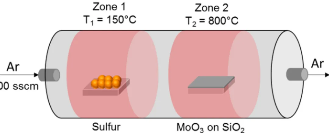
The thin molybdenum-oxide films on SiO2(900 nm)/Si substrates were obtained by DC magnetron sputtering from a Mo-target (using a Quorum Q300-TD system), followed by natural oxidation in air. The sulfurization process, schematically illustrated in Figure1, was carried out in a two-heating zones furnace (TSH12/38/500, Elite Thermal Systems Ltd., Market Harborough, UK), with the first zone (at a temperature of 150◦C) hosting a crucible with 300 mg sulphur (purity 99.9%, product 28260.234, VWR Chemicals, Radnor, PA, USA), and the second zone (at a temperature of 800◦C) hosting the MoO3/SiO2/Si sample. Starting from a base pressure of 4×10⁻⁶bar, the Ar carrier gas (purity 5.0, Messer, Budapest, Hungary) with a flux of 100 sccm transported the S vapours from the first to the second zone. The duration of the sulfurization process was 60 min.
play an important role in MoS2 formation during sulfurization of pre-deposited MoO3. In fact, while a higher temperature may enhance the sulfurization degree, on the other hand, it can also result in increased MoO3 evaporation and diffusion of Mo atoms on the substrate surface. This latter phenomenon strongly depends on the adhesion energy and surface diffusivity of Mo atoms on the substrate.
The main disadvantage of the continuous MoS2 films produced by the sulfurization approach is their nanocrystalline structure (with 20–30 nm grain-size) [44], typically resulting in poorer carrier mobility, if compared to the large and isolated monocrystalline MoS2 flakes obtained by the CVD approach. However, the high uniformity and its good compatibility with the fabrication methods used in the semiconductor industry makes this approach appealing for some applications, e.g., MoS2/semiconductor heterojunctions [52]
or hydrogen evolution applications [53]. Hence, a detailed characterisation of structural/compositional, vibrational, optical, and electrical properties of MoS2 films produced by Mo sulfurization remains highly desirable.
In this paper, few or multilayer MoS2 on a SiO2/Si substrate have been produced by sulfurization at 800 °C of very thin MoO3 films, from ~2.8 nm to ~4.2 nm (i.e., the critical range for the transition from horizontally to vertically aligned layers). The compositional, morphological, structural, electrical, and optical emission properties of the grown films have been extensively investigated by the combination of several characterisation techniques with macro to nanoscale spatial resolution. This correlative analysis provides deep insight into the potentialities and limitations of this material system for applications.
2. Materials and Methods
The thin molybdenum-oxide films on SiO2 (900 nm)/Si substrates were obtained by DC magnetron sputtering from a Mo-target (using a Quorum Q300-TD system), followed by natural oxidation in air. The sulfurization process, schematically illustrated in Figure 1, was carried out in a two-heating zones furnace (TSH12/38/500, Elite Thermal Systems Ltd., Market Harborough, UK), with the first zone (at a temperature of 150 °C) hosting a crucible with 300 mg sulphur (purity 99.9%, product 28260.234, VWR Chemicals, Radnor, PA, USA), and the second zone (at a temperature of 800 °C) hosting the MoO3/SiO2/Si sample. Starting from a base pressure of 4 × 10⁻⁶ bar, the Ar carrier gas (purity 5.0, Messer, Budapest, Hungary) with a flux of 100 sccm transported the S vapours from the first to the second zone. The duration of the sulfurization process was 60 min.
Figure 1. Schematic illustration of the sulfurization process of the thin MoO3 films on the SiO2/Si substrates.
Morphological analyses on the as-deposited MoO3 films and after the sulfurization process were carried out by Tapping mode Atomic Force Microscopy using a DI3100 system by Bruker (Santa Barbara, CA, USA) with Nanoscope V electronics. The compositional properties of the as-deposited metal films and MoS2 formation after the
Figure 1.Schematic illustration of the sulfurization process of the thin MoO3films on the SiO2/Si substrates.
Morphological analyses on the as-deposited MoO3films and after the sulfurization process were carried out by Tapping mode Atomic Force Microscopy using a DI3100 system by Bruker (Santa Barbara, CA, USA) with Nanoscope V electronics. The compositional properties of the as-deposited metal films and MoS2 formation after the sulfurization process were evaluated by X-ray photoelectron spectroscopy (XPS) using Escalab Xi+
equipment by Thermo Fisher (Waltham, MA, USA), with a monochromatic Al KαX-ray source (energy = 1486.6 eV). The spectra were collected at a take-off angle of 90◦relative to the sample surface and pass energy of 20 eV. The instrument resolution was 0.45 eV (FWHM of the Ag 3d5/2peak). The spectra were aligned using C1s (285 eV) as reference.
Nanomaterials2022,12, 182 4 of 15
High-resolution transmission electron microscopy (HR-TEM), high angle annular dark- field scanning transmission electron microscopy (HAADF-STEM), and energy dispersion spectroscopy (EDS) analyses of the MoS2thin films were carried out with an aberration- corrected Titan Themis 200 microscope by Thermo Fisher (Waltham, MA USA). To this aim, cross-sectioned samples were prepared by a focused ion beam (FIB). Raman spectroscopy and mapping of MoS2vibrational peaks were carried out by WiTec Alpha equipment by WiTec (Ulm, Germany), using laser excitation at 532 nm, 1.5 mW power, and 100×objective.
Photoluminescence spectra (PL) were collected using a Horiba (Palaiseau, France) system with a laser source of 532 nm. To confirm the uniformity of the MoS2thin layer across the substrate, the Raman and PL analyses have been performed at different positions on the sample. Finally, nanoscale resolution current mapping of MoS2on SiO2was per- formed by conductive Atomic Force Microscopy (C-AFM) with a DI3100 system by Bruker (Santa Barbara, CA, USA), using Pt-coated Si tips with ~5 nm curvature radius.
3. Results and Discussion
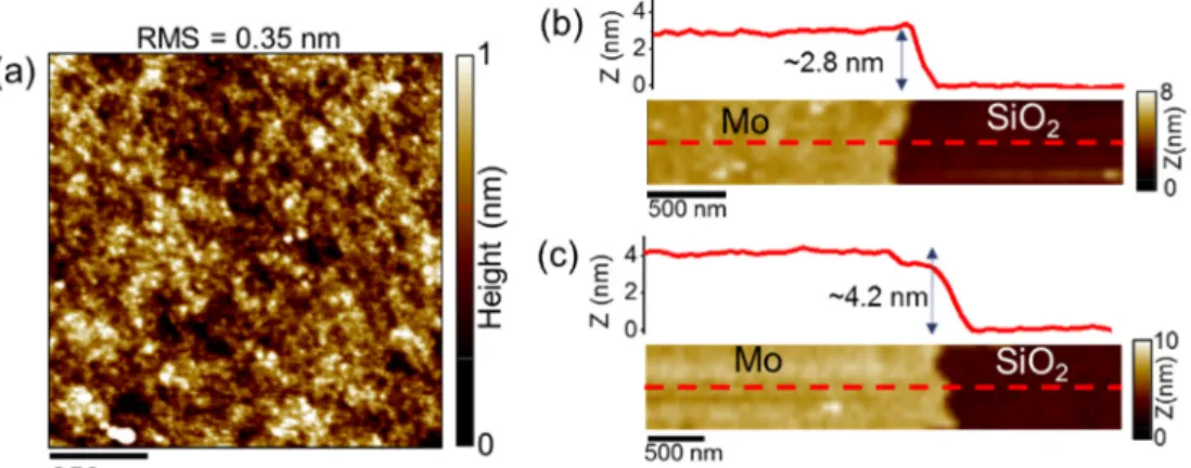
Figure2a shows a typical AFM morphology of as-deposited MoO3on the SiO2/Si substrate using the lowest sputtering time (30 s). This analysis indicates a very low root mean square (RMS) surface roughness of 0.35 nm. Similar roughness values have been measured for MoO3film thicknesses deposited at higher sputtering times. The thickness of the as-deposited films was also evaluated by AFM step height measurements performed on intentionally scratched regions of the films. Figure2b,c show the morphologies and corresponding line profiles for films deposited with two different sputtering times (30 s and 45 s), resulting in ~2.8 nm and ~4.2 nm thickness, respectively.
Nanomaterials 2022, 12, x FOR PEER REVIEW 4 of 16
sulfurization process were evaluated by X-ray photoelectron spectroscopy (XPS) using Escalab Xi+ equipment by Thermo Fisher (Waltham, MA, USA), with a monochromatic Al Kα X-ray source (energy = 1486.6 eV). The spectra were collected at a take-off angle of 90° relative to the sample surface and pass energy of 20 eV. The instrument resolution was 0.45 eV (FWHM of the Ag 3d5/2 peak). The spectra were aligned using C1s (285 eV) as reference. High-resolution transmission electron microscopy (HR-TEM), high angle annu- lar dark-field scanning transmission electron microscopy (HAADF-STEM), and energy dispersion spectroscopy (EDS) analyses of the MoS2 thin films were carried out with an aberration-corrected Titan Themis 200 microscope by Thermo Fisher (Waltham, MA USA). To this aim, cross-sectioned samples were prepared by a focused ion beam (FIB).
Raman spectroscopy and mapping of MoS2 vibrational peaks were carried out by WiTec Alpha equipment by WiTec (Ulm, Germany), using laser excitation at 532 nm, 1.5 mW power, and 100× objective. Photoluminescence spectra (PL) were collected using a Horiba (Palaiseau, France) system with a laser source of 532 nm. To confirm the uniformity of the MoS2 thin layer across the substrate, the Raman and PL analyses have been performed at different positions on the sample. Finally, nanoscale resolution current mapping of MoS2 on SiO2 was performed by conductive Atomic Force Microscopy (C-AFM) with a DI3100 system by Bruker (Santa Barbara, CA, USA), using Pt-coated Si tips with ~5 nm curvature radius.
3. Results and Discussion
Figure 2a shows a typical AFM morphology of as-deposited MoO3 on the SiO2/Si sub- strate using the lowest sputtering time (30 s). This analysis indicates a very low root mean square (RMS) surface roughness of 0.35 nm. Similar roughness values have been meas- ured for MoO3 film thicknesses deposited at higher sputtering times. The thickness of the as-deposited films was also evaluated by AFM step height measurements performed on intentionally scratched regions of the films. Figure 2b,c show the morphologies and cor- responding line profiles for films deposited with two different sputtering times (30 s and 45 s), resulting in ~2.8 nm and ~4.2 nm thickness, respectively.
Figure 2. (a) Typical AFM morphology of as-deposited MoO3 thin films on SiO2, with the indication of the root mean square (RMS) roughness. (b,c) Determination of the thickness of films deposited with two different sputtering times by measurement of the step heights (~2.8 nm and ~4.2 nm) with respect to SiO2 on scratched regions.
XPS compositional analyses performed on the thinnest deposited films revealed that they are predominantly composed of MoO3, with a small (<1%) MoO2 contribution. Re- cently, Vangelista et al. [44] also reported the complete oxidation (ascribed to air exposure after the deposition) of evaporated Mo films with similar thickness, used for subsequent MoS2 growth by sulfurization. The same authors [44] explained the conversion of MoO3 to MoS2 upon exposure to sulphur according to the following chemical reaction:
Figure 2.(a) Typical AFM morphology of as-deposited MoO3thin films on SiO2, with the indication of the root mean square (RMS) roughness. (b,c) Determination of the thickness of films deposited with two different sputtering times by measurement of the step heights (~2.8 nm and ~4.2 nm) with respect to SiO2on scratched regions.
XPS compositional analyses performed on the thinnest deposited films revealed that they are predominantly composed of MoO3, with a small (<1%) MoO2contribution. Re- cently, Vangelista et al. [44] also reported the complete oxidation (ascribed to air exposure after the deposition) of evaporated Mo films with similar thickness, used for subsequent MoS2growth by sulfurization. The same authors [44] explained the conversion of MoO3to MoS2upon exposure to sulphur according to the following chemical reaction:
2 MoO3(s) + 7 S(g)→2 MoS2(s) + 3 SO2(g), (1) which is the result of two intermediate steps:
MoO3+(x/2) S→MoO3−x+ (x/2) SO2 (2) MoO3−x+ [(7−x)/2] S→MoS2+ [(3−x)/2] SO2 (3)
Nanomaterials2022,12, 182 5 of 15
i.e., the S-induced reduction of the MoO3to a sub-stoichiometric oxide MoO3−x(2), fol- lowed by its conversion to MoS2(3), with the formation of gaseous SO2as a by-product.
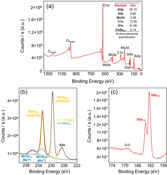
After the sulfurization process at 800◦C, XPS analyses were performed to evaluate the successful conversion of MoO3to MoS2. Figure3a reports an overview spectrum, allowing the quantification of the percentage of elemental concentrations on the sample surface. In particular, molybdenum and sulphur percentages of 3.26% and 6.82%, respectively, were evaluated (besides the large Si and O background), which were close to the stoichiometric [Mo]/[S] ratio for MoS2.More detailed information on the Mo and S bonding was deduced from the Mo3d3/2, Mo3d5/2, and S2s core levels in Figure3b, and the S2p1/2and S2p3/2 core levels in Figure3c. Two doublets were found in the Mo 3d spectrum, and both doublets were fitted with a peak separation of 3.1 eV [44,54,55]. In particular, the deconvolution of the Mo3d peaks shows the predominance of the Mo4+ component, associated with 2H-MoS2,accompanied by a smaller Mo6+contribution, associated with the presence of residual MoO3. The two S2p1/2 and S2p3/2 peaks [44,54,55] in Figure3c confirm that sulphur is mainly in the form of sulphide, with a small S-O component.
2 MoO3(s) + 7 S(g) → 2 MoS2(s) + 3 SO2(g), (1) which is the result of two intermediate steps:
MoO3 +(x/2) S → MoO3-x +(x/2) SO2 (2) MoO3-x +[(7 − x)/2] S → MoS2 +[(3 − x)/2] SO2 (3) i.e., the S-induced reduction of the MoO3 to a sub-stoichiometric oxide MoO3−x (2), followed by its conversion to MoS2 (3), with the formation of gaseous SO2 as a by-product.
After the sulfurization process at 800 °C, XPS analyses were performed to evaluate the successful conversion of MoO3 to MoS2. Figure 3a reports an overview spectrum, al- lowing the quantification of the percentage of elemental concentrations on the sample sur- face. In particular, molybdenum and sulphur percentages of 3.26% and 6.82%, respec- tively, were evaluated (besides the large Si and O background), which were close to the stoichiometric [Mo]/[S] ratio for MoS2. More detailed information on the Mo and S bond- ing was deduced from the Mo3d3/2, Mo3d5/2, and S2s core levels in Figure 3b, and the S2p1/2 and S2p3/2 core levels in Figure 3c. Two doublets were found in the Mo 3d spectrum, and both doublets were fitted with a peak separation of 3.1 eV [44,54,55]. In particular, the deconvolution of the Mo3d peaks shows the predominance of the Mo4+ component, asso- ciated with 2H-MoS2, accompanied by a smaller Mo6+ contribution, associated with the presence of residual MoO3. The two S2p1/2 and S2p3/2 peaks [44,54,55] in Figure 3c confirm that sulphur is mainly in the form of sulphide, with a small S-O component.
Figure 3.(a) Survey XPS spectrum of MoS2on SiO2produced by sulfurization of the 2.8 nm MoO3 film, with the indication of the evaluated surface elemental composition. (b) XPS spectra of the Mo 3d and S 2s core levels, with the deconvolution of the Mo4+contribution (related to MoS2) and the Mo6+
contribution (related to residual MoO3). (c) S 2p core levels spectra, indicating the predominance of the sulphide contribution, with a small S-O component.
Nanomaterials2022,12, 182 6 of 15
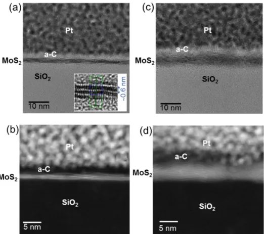
The structural properties of the MoS2films were also investigated at nanoscale by transmission electron microscopy on cross-sectioned samples. Figure4a,b show represen- tative HR-TEM and HAADF-STEM analyses on the few-layers MoS2sample obtained by sulfurization of the ~2.8 nm MoO3film. The diffraction contrast in the HR-TEM image Figure4a demonstrates the presence of two or three crystalline layers embedded between the amorphous SiO2substrate and amorphous carbon (a–c) protective film. These layers are predominantly oriented parallel to the substrate, with nanometric scale corrugations.
Furthermore, an interlayer spacing of ~0.6 nm is directly evaluated from the HRTEM image of a 3L-MoS2reported in the insert of Figure4a. The number of MoS2layers and their nearly parallel orientation with respect to the substrate is confirmed by the HAADF-STEM image in Figure4b collected on the same sample. On the other hand, a more irregular configuration of the layers can be observed from the HRTEM (Figure4c) and HAADF- STEM (Figure4d) analyses performed on the MoS2multilayer produced by sulfurization of
~4.2 nm film. In fact, in the analysed specimen volume, horizontally oriented MoS2layers co-exist with layers standing up with respect to the SiO2surface. This observation is fully consistent with previous reports showing a transition from horizontal to vertically oriented growth for film thickness larger than 3 nm [47].
Nanomaterials 2022, 12, x FOR PEER REVIEW 6 of 16
Figure 3. (a) Survey XPS spectrum of MoS2 on SiO2 produced by sulfurization of the 2.8 nm MoO3 film, with the indication of the evaluated surface elemental composition. (b) XPS spectra of the Mo 3d and S 2s core levels, with the deconvolution of the Mo4+ contribution (related to MoS2) and the Mo6+ contribution (related to residual MoO3). (c) S 2p core levels spectra, indicating the predomi- nance of the sulphide contribution, with a small S-O component.
The structural properties of the MoS2 films were also investigated at nanoscale by transmission electron microscopy on cross-sectioned samples. Figure 4a,b show repre- sentative HR-TEM and HAADF-STEM analyses on the few-layers MoS2 sample obtained by sulfurization of the ~2.8 nm MoO3 film. The diffraction contrast in the HR-TEM image Figure 4a demonstrates the presence of two or three crystalline layers embedded between the amorphous SiO2 substrate and amorphous carbon (a–c) protective film. These layers are predominantly oriented parallel to the substrate, with nanometric scale corrugations.
Furthermore, an interlayer spacing of ~0.6 nm is directly evaluated from the HRTEM im- age of a 3L-MoS2 reported in the insert of Figure 4a. The number of MoS2 layers and their nearly parallel orientation with respect to the substrate is confirmed by the HAADF-STEM image in Figure 4b collected on the same sample. On the other hand, a more irregular configuration of the layers can be observed from the HRTEM (Figure 4c) and HAADF- STEM (Figure 4d) analyses performed on the MoS2 multilayer produced by sulfurization of ~4.2 nm film. In fact, in the analysed specimen volume, horizontally oriented MoS2 lay- ers co-exist with layers standing up with respect to the SiO2 surface. This observation is fully consistent with previous reports showing a transition from horizontal to vertically oriented growth for film thickness larger than 3 nm [47].
Figure 4. Cross sectional HR-TEM (a) and HAADF-STEM (b) images of few-layers MoS2 obtained by sulfurization of the ~2.8 nm MoO3 film on the SiO2 substrate. MoS2 is composed by nearly hori- zontally aligned 2–3 layers. The interlayer spacing in a 3-layers region is evaluated from the HR- TEM in the insert of panel (a). Cross sectional HR-TEM (c) and HAADF-STEM (d) of multilayers MoS2 obtained by sulfurization of the ~4.2 nm MoO3 film.
Figure 4.Cross sectional HR-TEM (a) and HAADF-STEM (b) images of few-layers MoS2obtained by sulfurization of the ~2.8 nm MoO3film on the SiO2 substrate. MoS2 is composed by nearly horizontally aligned 2–3 layers. The interlayer spacing in a 3-layers region is evaluated from the HR-TEM in the insert of panel (a). Cross sectional HR-TEM (c) and HAADF-STEM (d) of multilayers MoS2obtained by sulfurization of the ~4.2 nm MoO3film.
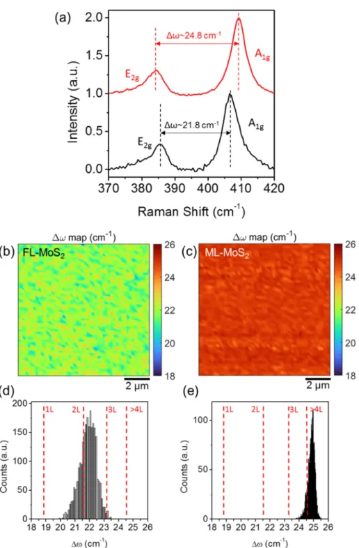
The layers number uniformity of the grown MoS2films was also investigated on micro- meter scale areas and with high statistics by Raman spectroscopy. Figure5shows two typical Raman spectra of the few-layers (i.e., 2 L–3 L) MoS2(black line) and of the multilayer MoS2(red line) grown on SiO2by the sulfurization process. The two characteristic in-plane (E2g) and out-of-plane (A1g) vibrational modes of MoS2 are clearly identified, and the typical redshift of the E2g peak and blue shift of the A1g with increasing the number
Nanomaterials2022,12, 182 7 of 15
of layers [19] is observed. In particular, the difference ∆ω= ωA1g−ωE2gbetween the wavenumbers of these two main modes is commonly taken as a way to evaluate the number of MoS2layers, with larger∆ωvalues generally associated with a thicker MoS2.
The layers number uniformity of the grown MoS2 films was also investigated on mi- cro-meter scale areas and with high statistics by Raman spectroscopy. Figure 5 shows two typical Raman spectra of the few-layers (i.e., 2 L–3 L) MoS2 (black line) and of the multi- layer MoS2 (red line) grown on SiO2 by the sulfurization process. The two characteristic in-plane (E2g) and out-of-plane (A1g) vibrational modes of MoS2 are clearly identified, and the typical redshift of the E2g peak and blue shift of the A1g with increasing the number of layers [19] is observed. In particular, the difference Δω = ω − ω between the wave- numbers of these two main modes is commonly taken as a way to evaluate the number of MoS2 layers, with larger Δω values generally associated with a thicker MoS2.
Figure 5. (a) Representative Raman spectra of the few-layers (FL) MoS2 (black-line) and multilayer (ML) MoS2 samples obtained by sulfurization of the 2.8 and 4.2 nm MoO3 films on SiO2. Colour Figure 5.(a) Representative Raman spectra of the few-layers (FL) MoS2(black-line) and multilayer (ML) MoS2samples obtained by sulfurization of the 2.8 and 4.2 nm MoO3films on SiO2. Colour maps of the A1g-E2gwavenumber difference∆ωobtained from arrays of Raman spectra collected on 10µm×10µm scan areas on the FL-MoS2(b) and on the ML-MoS2(c) samples. Histogram of∆ω values showing a distribution with a peak atω≈21.8±0.6 cm−1for the FL-MoS2sample associated to 2 L–3 L MoS2(d) andω≈24.8±0.4 cm−1for the ML-MoS2sample, corresponding to >4 L MoS2
thickness (e).
Nanomaterials2022,12, 182 8 of 15
The colour maps in Figure 5b,c illustrate the spatial distribution of the∆ωvalues obtained from arrays of 50×50 Raman spectra collected on 10µm×10µm scan areas.
Figure5d,e show the histograms of the∆ω values reported in the two maps, with the indication of the corresponding number of MoS2layers according to the calibration reported in Ref. [19]. The two distributions are quite uniform and exhibit aω≈21.8±0.6 cm−1 for the few-layer MoS2sample andω≈24.8±0.4 cm−1for the multilayer MoS2sample.
These∆ωvalues are associated with a 2 L–3 L MoS2thickness for the first sample, in very good agreement with TEM analyses in Figure4, and to >4 L MoS2for the second one.
In the following, we will concentrate our attention on the 2 L–3 L MoS2sample, since the horizontal configuration of the layers makes it more suitable for electronic applications, similarly to 2H-MoS2samples produced by CVD or by exfoliation from bulk molybdenite.
The doping type and the biaxial strain (ε) of the thin MoS2film were also evaluated from the Raman maps by a correlative plot of A1gversus E2gpeaks positions, as recently discussed in Ref. [23]. Figure6a shows as blue circles theωA1gandωE2gvalues extracted from all the Raman spectra in the array of Figure5. The red line in Figure6a represents the idealωA1gvs.ωE2gdependence (i.e., the strain line) for a purely strained 3L-MoS2film.
This relation is obtained from the combination of the following two expressions:
ωE2g =ω0E2g−2γE2gω0E2gε (4) ωA1g =ω0A1g−2γA
1gω0A1gε (5)
Here,γE2g = 0.39 andγA
1g = 0.09 are the Grüneisen parameters for the two vibra- tional modes of 3L-MoS2, estimated from the literature values of the peaks shift rates as a function of strain percentage (−3 cm−1/% and−0.7 cm−1/% for the E2gand A1gpeaks, respectively) [56]. ωE0
2g andωA0
1g represent the E2gand A1g frequencies for an ideally unstrained and undoped 3L-MoS2. Here, the literature values for a suspended 3L-MoS2
membrane (ω0E2g =382.9 cm−1andω0A1g =406.4 cm−1) [56], not affected by the inter- action with the substrate, were taken as the best approximation for these ideal values.
This reference point is reported as a red square in Figure6a, while the two arrows with opposite directions along the strain line indicate the tensile (red-shift) and compressive strain (blue-shift), respectively. Furthermore, the black dashed lines serve as guides to estimate the strain values. The distribution of the experimental points (blue circles) in the plot of Figure6a clearly indicates that the thin MoS2film on SiO2is compressively strained.
Figure6b shows the 2D map of the compressive strain, calculated from the map ofωE2g values by applying Equation (4). Furthermore, the corresponding histogram of theεvalues is reported in Figure6c, from which an average strain valueε≈ −0.78%±0.18% can be deduced.
The strain line separates the n-type and p-type doping regions in theωA1g−ωE2g diagram in Figure6a. Noteworthy, the experimental points in Figure 6a are partially located in the n-type region and partially in the p-type one. Unintentional n-type doping is typically reported for MoS2films produced by different synthesis methods (such as mechanical exfoliation or CVD) and it is commonly ascribed to native defects present in the material [57–60]. Here, the observed p-type doping in some regions of the MoS2
film produced by sulfurization can be associated with the presence of residual MoO3, as deduced by XPS. In fact, several studies demonstrated how intentionally introducing MoO3
in pristine (n-type) MoS2, e.g., by O2plasma treatments, results in p-type doping of the material [61,62].
Figure 6. (a) Correlative plot of the ωA1g and ωE2g values (blue circles) extracted from all the Raman spectra in the array of Figure 5. The red line represents the ideal ωA1g vs. ωE2g dependence (i.e., the strain line) for a purely strained 3L-MoS2 film. The red square corresponds to the frequencies ω and ω foran ideally unstrained and undoped 3L-MoS2, while the two red arrows with opposite directions along the strain line indicate the tensile (red-shift) and compressive strain (blue-shift), respectively. (b) Map and (c) corresponding histogram of the compressive strain on a 10 μm × 10 μm area.
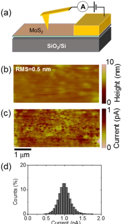
The MoS2 thin layers produced by MoO3 thin films sulfurization exhibit large resis- tivity values in the range of 10–100 Ω∙cm [63]. This can be ascribed, in part, to the nano- crystalline structure of the films, i.e., the large density of grain boundaries, which are known to introduce resistive contributions in the current path [64]. On the other hand, the local changes in the compressive strain distribution, as well in the carrier density, deduced by Raman mapping is expected to have an effect on the electrical properties of the few- layers of MoS2. To get direct information on the homogeneity of conductivity in this film, local current mapping has been carried out by C-AFM, as schematically depicted in Figure 7a. In this configuration, the current locally injected from the AFM metal tip flows in the MoS2 film and is finally collected from the macroscopic front contact. Due to the nanoscale size of the tip contact, the dominant contributions to the measured resistance are repre- sented by the local tip/MoS2 contact resistance and the spreading resistance in the MoS2
region underneath the tip. Figure 7b shows the contact-mode morphological image on the sample surface, from which an RMS roughness ≈ 0.5 nm slightly higher than the one of the as-deposited MoO3 film (Figure 2a) was deduced. Figure 7c,d report the correspond- ing C-AFM current map and the histogram of the measured current values. The current map clearly shows submicrometer lateral variations of the conductivity, which are only partially correlated to the morphology, while the histogram shows a Gaussian
Figure 6.(a) Correlative plot of theωA1gandωE2gvalues (blue circles) extracted from all the Raman spectra in the array of Figure5. The red line represents the idealωA1gvs.ωE2gdependence (i.e., the strain line) for a purely strained 3L-MoS2film. The red square corresponds to the frequenciesωE0
2g
andωA0
1gfor an ideally unstrained and undoped 3L-MoS2, while the two red arrows with opposite directions along the strain line indicate the tensile (red-shift) and compressive strain (blue-shift), respectively. (b) Map and (c) corresponding histogram of the compressive strain on a 10µm×10µm area.
The MoS2thin layers produced by MoO3thin films sulfurization exhibit large re- sistivity values in the range of 10–100Ω·cm [63]. This can be ascribed, in part, to the nanocrystalline structure of the films, i.e., the large density of grain boundaries, which are known to introduce resistive contributions in the current path [64]. On the other hand, the local changes in the compressive strain distribution, as well in the carrier density, deduced by Raman mapping is expected to have an effect on the electrical properties of the few-layers of MoS2. To get direct information on the homogeneity of conductivity in this film, local current mapping has been carried out by C-AFM, as schematically depicted in Figure7a. In this configuration, the current locally injected from the AFM metal tip flows in the MoS2film and is finally collected from the macroscopic front contact. Due to the nanoscale size of the tip contact, the dominant contributions to the measured resistance are represented by the local tip/MoS2contact resistance and the spreading resistance in the MoS2region underneath the tip. Figure7b shows the contact-mode morphological image on the sample surface, from which an RMS roughness≈0.5 nm slightly higher than the one of the as-deposited MoO3film (Figure2a) was deduced. Figure7c,d report the corresponding C-AFM current map and the histogram of the measured current values.
The current map clearly shows submicrometer lateral variations of the conductivity, which are only partially correlated to the morphology, while the histogram shows a Gaussian distribution of these values, resembling the shape of the strain distribution in Figure7d.
From this comparison, we can speculate that these mesoscopic-scale inhomogeneities can
Nanomaterials2022,12, 182 10 of 15
be partially ascribed to the lateral changes in the strain and carrier density detected by Raman.
Nanomaterials 2022, 12, x FOR PEER REVIEW 10 of 16
distribution of these values, resembling the shape of the strain distribution in Figure 7d.
From this comparison, we can speculate that these mesoscopic-scale inhomogeneities can be partially ascribed to the lateral changes in the strain and carrier density detected by Raman.
Figure 7. (a) Schematic of the C-AFM setup for local conductivity mapping of few-layers MoS2 on SiO2. (b) Morphology and (c) current map simultaneously measured with tip-to-sample bias of 5 V.
(d) Histogram of current values from the C-AFM map.
Figure 7.(a) Schematic of the C-AFM setup for local conductivity mapping of few-layers MoS2on SiO2. (b) Morphology and (c) current map simultaneously measured with tip-to-sample bias of 5 V.
(d) Histogram of current values from the C-AFM map.
In the last section of this paper, Raman and photoluminescence spectra acquired on the few-layers MoS2samples produced by sulfurization have been compared with reference spectra acquired on CVD-grown MoS2samples with a similar thickness.
Figure8shows a typical Raman spectrum of 3L-MoS2on SiO2produced by MoO3
sulfurization, compared with a spectrum of a 3L-MoS2sample grown by CVD on SiO2[65], reported as reference. Some remarkable differences can be clearly observed between MoS2
layers prepared using the two different approaches. In fact, besides a lower E2g/A1g
intensity ratio, the two vibrational peaks exhibit a more pronounced asymmetric shape in the 3L-MoS2 produced by sulfurization as compared to the CVD-grown one. The
Nanomaterials2022,12, 182 11 of 15
deconvolution analysis of the Raman spectra with four Gaussian contributions, associated with the main E2gand A1gmodes and the disorder activated LO(M) and ZO(M) modes [66], is also presented in Figure8. These LO(M) and ZO(M) components are very small in the Raman spectra of CVD 3L-MoS2, whereas their weight is higher in the 3L-MoS2produced by sulfurization. In this latter case, they can be ascribed both to the nanocrystalline nature of the film, as well as to the presence of residual MoO3, as deduced from the XPS analyses.
In the last section of this paper, Raman and photoluminescence spectra acquired on the few-layers MoS2 samples produced by sulfurization have been compared with refer- ence spectra acquired on CVD-grown MoS2 samples with a similar thickness.
Figure 8 shows a typical Raman spectrum of 3L-MoS2 on SiO2 produced by MoO3 sulfurization, compared with a spectrum of a 3L-MoS2 sample grown by CVD on SiO2 [65], reported as reference. Some remarkable differences can be clearly observed between MoS2
layers prepared using the two different approaches. In fact, besides a lower E2g/A1g inten- sity ratio, the two vibrational peaks exhibit a more pronounced asymmetric shape in the 3L-MoS2 produced by sulfurization as compared to the CVD-grown one. The deconvolu- tion analysis of the Raman spectra with four Gaussian contributions, associated with the main E2g and A1g modes and the disorder activated LO(M) and ZO(M) modes [66], is also presented in Figure 8. These LO(M) and ZO(M) components are very small in the Raman spectra of CVD 3L-MoS2, whereas their weight is higher in the 3L-MoS2 produced by sul- furization. In this latter case, they can be ascribed both to the nanocrystalline nature of the film, as well as to the presence of residual MoO3, as deduced from the XPS analyses.
Figure 8. Raman spectrum for 3L-MoS2 produced by sulfurization (red), compared with a reference spectrum for CVD grown 3L-MoS2 (blue). Data for CVD 3L-MoS2 were adapted with permission from [65], copyright Elsevier 2020.
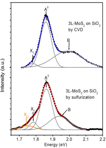
Figure 9 shows the comparison between a PL spectrum measured on the 3L-MoS2 produced by sulfurization with a reference spectrum for CVD grown 3L-MoS2, taken from Ref. [65]. For both spectra, acquired using a 532 nm wavelength laser source, the main emission peak at an energy of 1.86 eV can be observed. However, significant differences in spectral features can be clearly identified from a detailed deconvolution analysis.
Figure 8.Raman spectrum for 3L-MoS2produced by sulfurization (red), compared with a reference spectrum for CVD grown 3L-MoS2(blue). Data for CVD 3L-MoS2were adapted with permission from [65], copyright Elsevier 2020.
Figure9shows the comparison between a PL spectrum measured on the 3L-MoS2
produced by sulfurization with a reference spectrum for CVD grown 3L-MoS2, taken from Ref. [65]. For both spectra, acquired using a 532 nm wavelength laser source, the main emission peak at an energy of 1.86 eV can be observed. However, significant differences in spectral features can be clearly identified from a detailed deconvolution analysis.
The PL spectrum of CVD MoS2can be fitted by three Gaussian peaks, associated with the two exciton contributions (A0at 1.86±0.01 eV and B at 1.99±0.01 eV, due to the spin- orbit splitting of the valence band) and the trionic contribution (XTat 1.78±0.01 eV) [65].
On the other hand, the deconvolution analysis of the spectrum for the sulfurization grown sample allowed us to identify a fourth component XDat 1.75±0.01 eV, besides the trion (XT at 1.78±0.01 eV) and exciton peaks (A0at 1.86±0.01 eV and B at 1.95±0.01 eV).
Noteworthy, the presence of this XDcontribution is accompanied by a strong decrease in the spectral weight of the exciton peak B, as compared to the case of the CVD sample, as well as its FWHM reduction. The occurrence of a similar feature XD,associated with point defects in the MoS2lattice, has been recently reported by Chow et al. [67] for the PL spectra of MoS2flakes subjected to soft Ar-plasma irradiation, and it was also accompanied by a decrease in the exciton peak B with respect to unirradiated flakes. Hence, the observed XD contribution for our samples produced by sulfurization was ascribed to a higher density of point defects with respect to CVD grown samples.
Nanomaterials2022,12, 182 12 of 15
Nanomaterials 2022, 12, x FOR PEER REVIEW 12 of 16
Figure 9. Photoluminescence (PL) spectra for 3L-MoS2 produced by sulfurization, compared with a reference spectrum for CVD grown 3L-MoS2. The deconvolution analysis indicated the presence of the excitonic contributions A0, B, and of the trionic contribution XT (grey lines) for the CVD grown sample. In addition, the defect-related peak XD (orange line) is identified in the sulfurization grown sample. Data for CVD 3L-MoS2 were adapted with permission from [65], copyright Elsevier 2020.
The PL spectrum of CVD MoS2 can be fitted by three Gaussian peaks, associated with the two exciton contributions (A0 at 1.86 ± 0.01 eV and B at 1.99 ± 0.01 eV, due to the spin- orbit splitting of the valence band) and the trionic contribution (XT at 1.78 ± 0.01 eV) [65].
On the other hand, the deconvolution analysis of the spectrum for the sulfurization grown sample allowed us to identify a fourth component XD at 1.75 ± 0.01 eV, besides the trion (XT at 1.78 ± 0.01 eV) and exciton peaks (A0 at 1.86 ± 0.01 eV and B at 1.95 ± 0.01 eV). Note- worthy, the presence of this XD contribution is accompanied by a strong decrease in the spectral weight of the exciton peak B, as compared to the case of the CVD sample, as well as its FWHM reduction. The occurrence of a similar feature XD, associated with point de- fects in the MoS2 lattice, has been recently reported by Chow et al. [67] for the PL spectra of MoS2 flakes subjected to soft Ar-plasma irradiation, and it was also accompanied by a decrease in the exciton peak B with respect to unirradiated flakes. Hence, the observed XD
contribution for our samples produced by sulfurization was ascribed to a higher density of point defects with respect to CVD grown samples.
Figure 9.Photoluminescence (PL) spectra for 3L-MoS2produced by sulfurization, compared with a reference spectrum for CVD grown 3L-MoS2. The deconvolution analysis indicated the presence of the excitonic contributions A0, B, and of the trionic contribution XT(grey lines) for the CVD grown sample. In addition, the defect-related peak XD(orange line) is identified in the sulfurization grown sample. Data for CVD 3L-MoS2were adapted with permission from [65], copyright Elsevier 2020.
4. Conclusions
In conclusion, we reported a detailed analysis of the compositional, morphological, structural, electrical, and optical emission properties of few or multilayer MoS2 on a SiO2/Si substrate produced by sulfurization of very thin MoO3 films at 800◦C. Both Raman mapping and TEM/STEM analyses showed the formation of 2–3 layers of MoS2
nearly aligned with the SiO2surface after sulfurization of the thinnest MoO3film, whereas multilayers of MoS2(partially standing up) were observed for the thicker MoO3film. The strain distribution in the few-layer MoS2on SiO2was evaluated by the correlative plot of the characteristic A1g-E2gRaman modes, showing the occurrence of a compressive strain ε≈ −0.78±0.18%. Furthermore, the co-existence of submicrometer areas with n- and p-type doping is detected, with the p-type doping probably due to the presence of residual MoO3, as revealed by XPS analyses. Nanoscale resolution current mapping by C-AFM showed conductivity inhomogeneities in the few-layer MoS2, which are well correlated to the lateral changes in the strain detected by Raman. Finally, the characteristics spectroscopic signatures of the defects/disorder were identified by comparing Raman and PL spectra of sulfurization grown MoS2with reference analyses of CVD-grown single crystalline MoS2. The demonstrated MoS2growth method is quite versatile and can be extended to different substrates, besides SiO2. In particular, the adoption of crystalline substrates (such as sapphire, GaN, and 4H-SiC) with the hexagonal basal plane and good lattice matching with MoS2 is expected to enhance the domain size and electronic quality of the grown films. Furthermore, the homogeneous large area few-layer MoS2can be transferred to
arbitrary substrates (including flexible ones) [68] and find applications in different fields of microelectronics, flexible electronics, and sensing.
Author Contributions:Conceptualization, F.G. and A.K.; methodology, A.K.; software, S.E.P.; formal analysis, S.E.P.; investigation, A.K., S.E.P., E.S., G.G., P.F., A.S., M.N., S.D.F., S.A., M.C. and B.P.;
resources, S.D.F.; data curation, S.E.P.; writing—original draft preparation, S.E.P.; writing—review and editing, all authors; supervision, F.G., B.P. and F.M.G.; project administration, F.G.; funding acquisition, F.G., B.P. and F.R. All authors have read and agreed to the published version of the manuscript.
Funding:This work was funded, in part, by MUR in the framework of the FlagERA-JTC 2019 project ETMOS. E.S. acknowledges the PON project EleGaNTe (ARS01_01007) funded by MUR for financial support. B.P acknowledges funding from the national project TKP2021-NKTA-05. Furthermore, B.P.
acknowledges VEKOP-2.3.3-15-2016-00002 of the European Structural and Investment Funds for providing the microscope facility. Part of the experiments was carried out using the facilities of the Italian Infrastructure Beyond Nano.
Institutional Review Board Statement:Not applicable.
Informed Consent Statement:Not applicable.
Data Availability Statement:The data that support the findings of this study are available from the corresponding author upon reasonable request.
Acknowledgments:We would like to acknowledge the Thermo Fisher Scientific Applications Labo- ratory, East Grinstead, UK, for providing XPS spectra on MoS2layers.
Conflicts of Interest:The authors declare no conflict of interest.
References
1. Manzeli, S.; Ovchinnikov, D.; Pasquier, D.; Yazyev, O.V.; Kis, A. 2D transition metal dichalcogenides.Nat. Rev. Mater.2017,2, 17033. [CrossRef]
2. Lopez-Sanchez, O.; Lembke, D.; Kayci, M.; Radenovic, A.; Kis, A. Ultrasensitive Photodetectors Based on Monolayer MoS2.Nat.
Nanotechnol.2013,8, 497–501. [CrossRef]
3. Yin, Z.; Li, H.; Li, H.; Jiang, L.; Shi, Y.; Sun, Y.; Lu, G.; Zhang, Q.; Chen, X.; Zhang, H. Single-Layer MoS2Phototransistors.ACS Nano2012,6, 74–80. [CrossRef] [PubMed]
4. Li, H.; Yin, Z.; He, Q.; Li, H.; Huang, X.; Lu, G.; Fam, D.W.H.; Tok, A.l.Y.; Zhang, Q.; Zhang, H. Fabrication of Single-and Multilayer MoS2Film-Based Field-Effect Transistors for Sensing NO at Room Temperature. Small2012,8, 63–67. [CrossRef]
[PubMed]
5. Radisavljevic, B.; Whitwick, M.B.; Kis, A. Integrated Circuits and Logic Operations Based on Single-Layer MoS2.ACS Nano2011, 5, 9934–9938. [CrossRef] [PubMed]
6. Ayari, A.; Cobas, E.; Ogundadegbe, O.; Fuhrer, M.S. Realization and Electrical Characterization of Ultrathin Crystals of Layered Transition-Metal Dichalcogenides.J. Appl. Phys.2007,101, 014507. [CrossRef]
7. Luo, Y.K.; Xu, J.; Zhu, T.; Wu, G.; McCormick, E.J.; Zhan, W.; Neupane, M.R.; Kawakami, R.K. Opto-Valleytronic Spin Injection in Monolayer MoS2/Few-Layer Graphene Hybrid Spin Valves.Nano Lett.2017,17, 3877–3883. [CrossRef]
8. Jiang, J.; Chen, Z.; Hu, Y.; Xiang, Y.; Zhang, L.; Wang, Y.; Wang, G.-C.; Shi, J. Flexo-photovoltaic effect in MoS2.Nat. Nanotechnol.
2021,16, 894–901. [CrossRef]
9. Hu, J.; Yu, L.; Deng, J.; Wang, Y.; Cheng, K.; Ma, C.; Zhang, Q.; Wen, W.; Yu, S.; Pan, Y.; et al. Sulfur vacancy-rich MoS2as a catalyst for the hydrogenation of CO2to methanol.Nat. Catal.2021,4, 242–250. [CrossRef]
10. Li, G.; Chen, Z.; Li, Y.; Zhang, D.; Yang, W.; Liu, Y.; Cao, L. Engineering Substrate Interaction To Improve Hydrogen Evolution Catalysis of Monolayer MoS2Films beyond Pt.ACS Nano2020,14, 1707–1714. [CrossRef]
11. Mak, K.F.; Lee, C.; Hone, J.; Shan, J.; Heinz, T.F. Atomically Thin MoS2: A New Direct-Gap Semiconductor.Phys. Rev. Lett.2010, 105, 136805. [CrossRef] [PubMed]
12. Kuc, A.; Zibouche, N.; Heine, T. Influence of Quantum Confinement on the Electronic Structure of the Transition Metal Sulfide TS2.Phys. Rev. B Condens. Matter Mater. Phys.2011,83, 245213. [CrossRef]
13. Radisavljevic, B.; Radenovic, A.; Brivio, J.; Giacometti, V.; Kis, A. Single-Layer MoS2 Transistors. Nat. Nanotechnol. 2011,6, 147–150. [CrossRef] [PubMed]
14. Wu, W.; De, D.; Chang, S.C.; Wang, Y.; Peng, H.; Bao, J.; Pei, S.S. High mobility and high on/off ratio field-effect transistors based on chemical vapor deposited single-crystal MoS2grains.Appl. Phys. Lett.2013,102, 142106. [CrossRef]
15. Yoon, Y.; Ganapathi, K.; Salahuddin, S. How Good Can Monolayer MoS2Transistors Be?Nano Lett.2011,11, 3768–3773. [CrossRef]
[PubMed]
Nanomaterials2022,12, 182 14 of 15
16. Giannazzo, F.; Greco, G.; Roccaforte, F.; Sonde, S.S. Vertical Transistors Based on 2D Materials: Status and Prospects.Crystals2018, 8, 70. [CrossRef]
17. Giannazzo, F. Engineering 2D heterojunctions with dielectrics.Nat. Electron.2019,2, 54. [CrossRef]
18. Novoselov, K.S.; Jiang, D.; Schedin, F.; Booth, T.J.; Khotkevich, V.V.; Morozov, S.V.; Geim, A.K. Two-dimensional atomic crystals.
Proc. Natl. Acad. Sci. USA2005,102, 10451–10453. [CrossRef]
19. Lee, C.; Yan, H.; Brus, L.E.; Heinz, T.F.; Hone, J.; Ryu, S. Anomalous lattice vibrations of single-and few-layer MoS2.ACS Nano 2010,4, 2695–2700. [CrossRef]
20. Velický, M.; Donnelly, G.E.; Hendren, W.R.; McFarland, S.; Scullion, D.; DeBenedetti, W.J.I.; Correa, G.C.; Han, Y.; Wain, A.J.;
Hines, M.A.; et al. Mechanism of Gold-Assisted Exfoliation of Centimeter-Sized Transition-Metal Dichalcogenide Monolayers.
ACS Nano2018,12, 10463–10472. [CrossRef]
21. Desai, S.B.; Madhvapathy, S.R.; Amani, M.; Kiriya, D.; Hettick, M.; Tosun, M.; Zhou, Y.; Dubey, M.; Ager, J.W., III; Chrzan, D.; et al.
Gold-Mediated Exfoliation of Ultralarge Optoelectronically-Perfect Monolayers.Adv. Mater.2016,28, 4053–4058. [CrossRef]
22. Magda, G.Z.; Pet˝o, J.; Dobrik, G.; Hwang, C.; Biró, L.P.; Tapasztó, L. Exfoliation of Large-Area Transition Metal Chalcogenide Single Layers.Sci. Rep.2015,5, 14714. [CrossRef]
23. Panasci, S.E.; Schilirò, E.; Migliore, F.; Cannas, M.; Gelardi, F.M.; Roccaforte, F.; Giannazzo, F.; Agnello, S. Substrate impact on the thickness dependence of vibrational and optical properties of large area MoS2produced by gold-assisted exfoliation.Appl. Phys.
Lett.2021,119, 093103. [CrossRef]
24. Panasci, S.E.; Schilirò, E.; Greco, G.; Cannas, M.; Gelardi, F.M.; Agnello, S.; Roccaforte, F.; Giannazzo, F. Strain, Doping, and Electronic Transport of Large Area Monolayer MoS2Exfoliated on Gold and Transferred to an Insulating Substrate.ACS Appl.
Mat. Interf.2021,13, 31248–31259. [CrossRef] [PubMed]
25. Coleman, J.N.; Lotya, M.; O’Neill, A.; Bergin, S.D.; King, P.J.; Khan, U.; Young, K.; Gaucher, A.; De, S.; Smith, R.J.; et al.
Two-dimensional nanosheets produced by liquid exfoliation of layered materials.Science2011,331, 568–571. [CrossRef] [PubMed]
26. Lee, Y.H.; Zhang, X.-Q.; Zhang, W.; Chang, M.-T.; Lin, C.-T.; Chang, K.-D.; Yu, Y.-C.; Wang, J.T.-W.; Chang, C.-S.; Li, L.-J.; et al.
Synthesis of Large-Area MoS2Atomic Layers with Chemical Vapor Deposition.Adv. Mater.2012,24, 2320–2325. [CrossRef]
27. Zhan, Y.; Liu, Z.; Najmaei, S.; Ajayan, P.M.; Lou, J. Large-Area Vapor-Phase Growth and Characterization of MoS2Atomic Layers on a SiO2Substrate.Small2012,8, 966–971. [CrossRef]
28. Ho, Y.-T.; Ma, C.-H.; Luong, T.-T.; Wei, L.-L.; Yen, T.-C.; Hsu, W.-T.; Chang, W.-H.; Chu, Y.-C.; Tu, Y.-Y.; Pande, K.P.; et al. Layered MoS2Grown on c-Sapphire by Pulsed Laser Deposition.Phys. Status Solidi RRL2015,9, 187–191. [CrossRef]
29. Fu, D.; Zhao, X.; Zhang, Y.-Y.; Li, L.; Xu, H.; Jang, A.-R.; Yoon, S.I.; Song, P.; Poh, S.M.; Ren, T.; et al. Molecular Beam Epitaxy of Highly Crystalline Monolayer Molybdenum Disulfide on Hexagonal Boron Nitride.J. Am. Chem. Soc.2017,139, 9392–9400.
[CrossRef]
30. Valdivia, A.; Tweet, D.J.; Conley, J.F., Jr. Atomic layer deposition of two dimensional MoS2on 150 mm substrates.J. Vac. Sci.
Technol.2016,34, 21515. [CrossRef]
31. Najmaei, S.; Liu, Z.; Zhou, W.; Zou, X.; Shi, G.; Lei, S.; Yakobson, B.I.; Idrobo, J.-C.; Ajayan, P.M.; Lou, J. Vapour phase growth and grain boundary structure of molybdenum disulphide atomic layers.Nat. Mater.2013,12, 754–759. [CrossRef] [PubMed]
32. Liu, H.F.; Wong, S.L.; Chi, D.Z. CVD growth of MoS2-based two-dimensional materials.Chem. Vap. Depos.2015,21, 241–259.
[CrossRef]
33. Jeon, J.; Jang, S.K.; Jeon, S.M.; Yoo, G.; Jang, Y.H.; Park, J.H.; Lee, S. Layer-controlled CVD growth of large-area two-dimensional MoS2films.Nanoscale2015,7, 1688–1695. [CrossRef] [PubMed]
34. Chen, J.; Tang, W.; Tian, B.; Liu, B.; Zhao, X.; Liu, Y.; Ren, T.; Liu, W.; Geng, D.; Jeong, H.Y.; et al. Chemical Vapor Deposition of High-Quality Large-Sized MoS2Crystals on Silicon Dioxide Substrates.Adv. Sci.2016,3, 1600033. [CrossRef] [PubMed]
35. Zhang, Z.; Chen, P.; Duan, X.; Zang, K.; Luo, J.; Duan, X. Robust epitaxial growth of two-dimensional heterostructures, multiheterostructures, and superlattices.Science2017,357, 788–792. [CrossRef]
36. Liu, B.; Fathi, M.; Chen, L.; Abbas, A.; Ma, Y.; Zhou, C. Chemical vapor deposition growth of monolayer WSe2with tunable device characteristics and growth mechanism study.ACS Nano2015,9, 6119–6127. [CrossRef]
37. Tang, L.; Tan, J.; Nong, H.; Liu, B.; Cheng, H.M. Chemical Vapor Deposition Growth of Two-Dimensional Compound Materials:
Controllability, Material Quality, and Growth Mechanism.Acc. Mater. Res.2020,2, 36–47. [CrossRef]
38. Wang, S.; Rong, Y.; Fan, Y.; Pacios, M.; Bhaskaran, H.; He, K.; Warner, J.H. Shape evolution of monolayer MoS2crystals grown by chemical vapor deposition.Chem. Mater.2014,26, 6371–6379. [CrossRef]
39. Yang, S.Y.; Shim, G.W.; Seo, S.B.; Choi, S.Y. Effective shape-controlled growth of monolayer MoS2 flakes by powder-based chemical vapor deposition.Nano Res.2017,10, 255–262. [CrossRef]
40. Wu, C.R.; Chang, X.R.; Wu, C.H.; Lin, S.Y. The growth mechanism of transition metal dichalcogenides by using sulfurization of pre-deposited transition metals and the 2D crystal hetero-structure establishment.Sci. Rep.2017,7, 42146. [CrossRef]
41. Li, D.; Xiao, Z.; Mu, S.; Wang, F.; Liu, Y.; Song, J.; Huang, X.; Jiang, L.; Xiao, J.; Liu, L.; et al. A facile space-confined solid-phase sulfurization strategy for growth of high-quality ultrathin molybdenum disulfide single crystals.Nano Lett.2018,18, 2021–2032.
[CrossRef] [PubMed]
42. Taheri, P.; Wang, J.; Xing, H.; Destino, J.F.; Arik, M.M.; Zhao, C.; Kang, K.; Blizzard, B.; Zhang, L.; Zhao, P. Growth mechanism of largescale MoS2monolayer by sulfurization of MoO3film.Mater. Res. Expr.2016,3, 075009. [CrossRef]

![Figure 8 shows a typical Raman spectrum of 3L-MoS 2 on SiO 2 produced by MoO 3 sulfurization, compared with a spectrum of a 3L-MoS 2 sample grown by CVD on SiO 2 [65], reported as reference](https://thumb-eu.123doks.com/thumbv2/9dokorg/731293.29132/11.892.254.628.274.675/figure-spectrum-produced-sulfurization-compared-spectrum-reported-reference.webp)