Journal Pre-proofs
Full Length Article
Design and production of tungsten-carbide rich coating layers A.S. Racz, Z. Fogarassy, U. Kentsch, P. Panjan, M. Menyhard
PII: S0169-4332(22)00396-8
DOI: https://doi.org/10.1016/j.apsusc.2022.152818
Reference: APSUSC 152818
To appear in: Applied Surface Science Received Date: 4 January 2022
Revised Date: 3 February 2022 Accepted Date: 10 February 2022
Please cite this article as: A.S. Racz, Z. Fogarassy, U. Kentsch, P. Panjan, M. Menyhard, Design and production of tungsten-carbide rich coating layers, Applied Surface Science (2022), doi: https://doi.org/10.1016/j.apsusc.
2022.152818
This is a PDF file of an article that has undergone enhancements after acceptance, such as the addition of a cover page and metadata, and formatting for readability, but it is not yet the definitive version of record. This version will undergo additional copyediting, typesetting and review before it is published in its final form, but we are providing this version to give early visibility of the article. Please note that, during the production process, errors may be discovered which could affect the content, and all legal disclaimers that apply to the journal pertain.
© 2022 Published by Elsevier B.V.
Design and production of tungsten-carbide rich coating layers.
A.S. Racz†, Z. Fogarassy†, U. Kentsch£, P. Panjan§, M. Menyhard†*
† Institute for Technical Physics and Materials Science, Centre for Energy Research, Konkoly Thege M. út 29-33, 1121 Budapest, Hungary
£ Helmholtz-Zentrum Dresden-Rossendorf, Bautzner Landstraße 400, 01328 Dresden - Germany
§ Jožef Stefan Institute, Jamova 39, 1000 Ljubljana, Slovenia
*Corresponding author: menyhard.miklos@ek-cer.hu ABSTRACT
Ion beam induced mixing (IBM) can be used for making protecting coating layers at room temperature. We have studied the production of tungsten-carbide, having high strength and low friction, by IBM since this material is also a candidate for protective coatings. WC rich layers have been produced by irradiating C/W multilayer of various structures (with individual layer thicknesses from 10 to 20 nm) by noble gases using medium energy projectiles. The resulting alterations of the samples have been measured by Auger electron spectroscopy (AES) depth- profiling. TRIDYN simulations, with some parametrization, were applied to determine the elemental in-depth distribution after IBM; the compound formation was calculated by a simple model. The calculated and measured depth profiles were compared and excellent agreement has been found for a rich dataset differing in layer structures, projectiles, ion fluences and energies.
The good agreement in a wide parameter range validates our procedure and allows the design of the WC-rich layers and also enables the significant decrease of the experimental work.
KEYWORDS: tungsten-carbide, WC, coating, simulation, ion irradiation, TRIDYN
1. INTRODUCTION
There is always a need for layer production methods which operate at not too high temperature. Ion beam mixing (IBM) is a layer production method which meets that requirement since it is a highly non-equilibrium process, which enables the reduction of the generally used
layer production temperature. E.g. Gupta et al. synthetized PbTe nanocrystals using low energy IBM of a Te/Pb bilayer on a Si substrate [1]. Arranz et al. investigated the mixing of Ti and Al layers [2]. Galindo et al. produced chromium-silicon mixed oxides by mixing of Cr/Si bilayer by oxygen atoms [3].
During IBM energetic ions hit the surface of materials they collide with atoms knocking some of them out from their position. The knocked-out atoms initiate further collisional processes, thus a collisional cascade develops, causing the mixing of the atoms in the effected region. Since during the cascade process the initial momentum of the projectile is lost in a short time the particles move, more or less isotopically, similar to that of usual diffusion. Thus, the equations of diffusion can be applied for the description of the IBM. The simplest and frequently occurring process is the ballistic intermixing when the atoms are ejected from their equilibrium position from the crystal lattice and transported to some nearby place forming a defect complex named Frenkel pair. The ensuing events can be described by binary interactions and the mixing can be described by the Fick equation consisting an apparent diffusion constant, resulting in the equation of 4Dt∼φ; where D is the effective diffusion coefficient t is the time and φ is the dose of the bombarding particle [4]. If the cascade does not cool down very fast, thermodynamical parameters also affect the diffusional movement; this process is called as thermal spike, which generally results in stronger mixing. In fact, the whole phenomenon, thermal spike mixing, was discovered in this way; it turned out that materials with high negative mixing enthalpy exhibit much stronger mixing efficiency than that predicted by the binary model [5]. This process can be described by applying the same equations, the only difference is the value of the effective diffusion constant. In case of thermal spike mixing the effective diffusion constant depends on the enthalpy of mixing (Darken) and is generally much higher than that in the ballistic process. In this case, depending on whether the individual cascades are overlapping or non-overlapping, the dependence on φ can be squared and linear, respectively. The simple rule of thumb is that in systems with low average atomic number (less than 20) and if the deposited energy is not too high, ballistic mixing occurs, while for systems with an average atomic number higher than 20 and higher deposited energy is applied, the thermal spike model operates [6]. The above is true in cases which result in an equilibrium or non- equilibrium mixture and/or alloy. However, IBM is strongly affected if compound formation occurs – and this adds to the complexity of the process. In this case new equations and distributions appear because of the changed diffusion and depending on the deposited energy both squared and
linear dependence of the mixing rate on the dose can be found [7,8]. It may also happen that instead of the diffusional mixing (obeying Fick’s law) a sharp interface between the mixed region moves [7,9] and layer formation occurs.
In cases when the aim is to produce a layer of desired thickness by IBM the use of multilayer structures is suggested [10,11]. The application of multilayers helps in tuning the thickness of the produced layer. The analytical equations of IBM do not work straightforwardly in these cases, thus for the prediction of the layer structure some other method is to be used.
Previously we have produced corrosion and wear resistant nano-layers by medium energy IBM of multilayer systems consisting pure Si and C layers [12–16]. This system, containing low atomic number elements is predicted to intermix by the ballistic process. It also turned out that in this system the mixing and compound formation process can be decoupled and thus TRYDIN simulation based on ballistic mixing processes could be successfully applied to describe the mixing and the subsequent compound formation could be described by a simple model [13,17]. Thus, the growth of the nano layer could be predicted by applying the above methods for a wide range of structural and ion bombardment conditions.
Tungsten carbide based nano layers have also several applications due to their superior hardness, low friction coefficient, and thermal stability [18,19]. Other interesting applications for WC rich thin and nano layers are found in microelectronics where tungsten carbides have been employed as a thin-film diffusion barrier and as Schottky contact for SiC-based high temperature electronics. Tungsten carbides have applications in heterogeneous catalysis, as well [20]. Since some of the applications need thin & nano layers to be produced at medium temperature it is of great interest, whether these structures can be produced by IBM of W/C multilayer systems.
Similarly to the Si/C system, it would also be very useful to have some means of predicting the layer growth process for various layer structures and ion bombardment conditions. In this case, however, the average atomic number, 40, is far above 20, thus, the ion mixing is expected to be governed by thermal spike, and consequently describing the IBM by means of TRIDYN simulation is questionable. An additional possibility might be the use of molecular dynamics (MD) simulation but its application for such systems due to the high computation time is far from straightforward.
Not having any other means, we still tried to apply the same approach as in the case of the Si/C system - based on that consideration that, in principle, the main difference between the ballistic
and thermal spike model is the strongly different effective diffusional constant. Our hope was that by simply increasing the value of the diffusional constant, the mixing could be estimated reasonable well by applying the TRIDYN simulation.
The aim of the article is twofold. First we show that it is possible to produce tungsten-carbide rich coating of various thicknesses by means of ion beam mixing of W/C mulilayers. Secondly we also demonstrate that the proposed simulation method works properly and thus it is possible to design custom made tungsten carbides based on the simulation. This work is also a first example for showing that the fast TRIDYN simulation can be applied for description thermal spike mixing at least for some material pairs. This might open new horizons for predicting the alteration of material due to IBM.
2. EXPERIMENTAL SECTION
2.1. Sample production and AES depth profiling
Several C/W multilayer structures were produced by sputtering on Si single crystal substrate in a Balzers Sputron sputtering chamber. The actual layer thicknesses of the specimens, determined by cross sectional electron microscopy (XTEM), were the following: C 10.4 nm / W 24.5 nm / C 9.1 nm / Si substrate; C 8 nm / W 18 nm / C 8.7 nm / W 18.6 nm / C 7.1 nm/ Si substrate; C 15.8 nm / W 22.7 nm / C 17.2 nm / W 24.3 nm / C 21.1 nm / Si substrate.
The WC-rich layers were produced by irradiating the multilayer structures by Ar+ or Xe+ ions at room temperature. The irradiation took place in Helmholtz-Zentrum Dresden-Rossendorf in a High Voltage Engineering Europa B.V., Model B8385 implanter. The applied energy for argon was 40-110 keV, the fluences were 0.1 - 6x10¹⁶ Ar+/cm2. In the case of xenon the energy varied between 40-160 keV, while the fluences were 0.07 - 3x10¹⁶ Xe+/cm2.
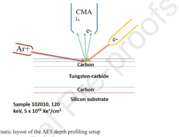
After ion irradiation, the sample was measured by AES depth profiling to obtain the composition distributions along the depth. The Auger spectra were recorded by a STAIB DESA 150 pre- retarded Cylindrical Mirror Analyzer (CMA) in direct current mode. For the depth profiling 1 keV Ar+ ions were used with an angle of incidence of 65° with respect to the surface normal, for avoiding large sputtering yield differences [21]. The ion current was kept constant during
sputtering. The sample was rotated (6 rev/min) during ion bombardment. These parameters were chosen for minimizing the ion bombardment-induced surface and interface morphology changes [22]. The schematic view of the experimental layout is shown in Fig. 1. The samples produced by ion beam mixing are irradiated by the electron beam. The emitted Auger electrons are detected by the CMA. For having the component in-depth distribution the sample is sputtered by argon ions.
Fig. 1. Schematic layout of the AES depth profiling setup
The detailed evaluation procedure of the AES depth profiles can be found in [21], its summary is as follows. The shapes and energies of the C (KLL) Auger peak in carbide and graphite phases are different, thus based on these differences the measured C Auger peak could be decomposed into graphitic and carbide components. The experimentally measured Auger peak decomposition has been performed by applying the CasaXPS program [23]. Hence the AES analysis provided the depth distributions of C, W, WC, and Si. The relative sensitivity factor method [24] was used for the calculation of the atomic concentrations. The relative sensitivity factors for C and W were determined from the intensities measured on pure C or W layers. The relative sensitivity factors for C emitted from WC were determined in a sample after irradiation where all C content was in carbide state. The same relative sensitivity factors were applied for each
evaluation of all measured AES spectra. As the tungsten has a strong backscattering factor, the intensity of carbon peak in the second C layer was lower than of the first one (counted from the surface). Similarly, the peak-to-peak intensity within the W layer slightly decreased along the depth. This dependence can be calculated [25] but in the present case we will use a simple approximation by linearly varying the backscattering factor resulting in a varying relative sensitivity factor. The sputtering time was transformed to the removed thickness by applying our previously elaborated method [26]. Its summary is as follows. The relative sputtering yields of pure C and W could be determined from the sputtering times required to remove the known layer thicknesses of the as-deposited W and C layers. In the regions that contain mixed C and W components (independently from their chemical state) we suppose that the total sputtering yield Y can be estimated as Y = ΣXi*Yi where Yi and Xi are the sputtering yield and concentration of component i (in our case ’C’ or ’W’). All presented in-depth distributions were calculated by this procedure.
2.2. Simulation of the tungsten carbide in-depth distribution
According to the experiments, medium energy ion bombardment of our sample (made of pure C and W layers) results in tungsten carbide production. Our aim was to simulate the WC in depth distribution as a function of irradiation (projectile, energy, fluence) and sample structure.
Our assumption is that the production of WC can be divided into two processes as a./ ion mixing and b./ subsequent compound formation.
The result of simulation is to be compared with the experimental results which are provided by AES depth profiling. AES depth profiling of the W/C/WC…multilayer, however, produces serious artefacts [21]. Thus, for the comparison of the simulated and measured depth profiles an additional simulation is to be applied; we should simulate the AES depth profile of the IBM modified sample.
2.2.1. Simulation of ion beam mixing of multilayer structure made of C and W layers
Based on the experimental results, we can conclude that a thick carbide layer forms if 40 keV Ar+ ion bombardment with fluence of 3x10¹⁶ ions/cm2 is applied to sample with structure of C 10 nm/ W 24.5 nm / C 9.1 nm /Si substrate, which means that the layers are fully intermixed.
Thus, to start with we will simulate the IBM for these ion bombardment parameters for the same layer structure.
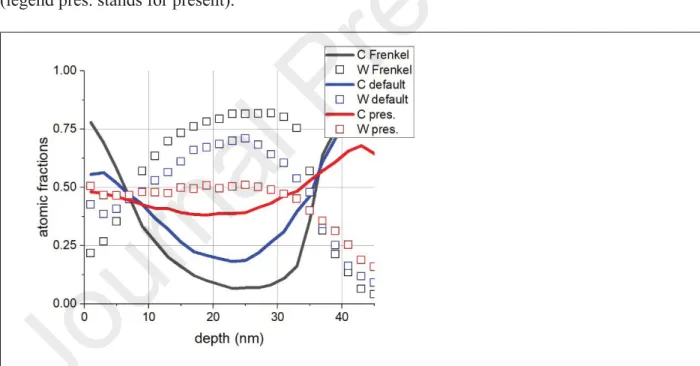
The strength of mixing in the TRIDYN simulation mainly depends on the value of the relocation threshold energy which can be varied by the user. The relocation threshold energy theoretically equals to the formation energy of Frenkel pair which are 38 eV, 25 eV and 13 eV for W, C and Si, respectively. Based on many comprehensive studies, the simulation provides much better agreement with the experiments if 8 eV is chosen for relocation threshold energy for all elements [27]. Fig. 2 shows distributions of C and W provided by the TRIDYN simulation after applying ion bombardment of 40 keV Ar+, 3x10¹⁶ ions/cm2 to sample with structure of C 10nm/W 24.5 nm / C 9.1 nm/ Si substrate, using the various relocation threshold energies mentioned before. It is clear, that neither choice of the relocation threshold energies (Frenkel pair energies, default values of TRIDYN) results in full intermixing. On the other hand, if we choose 2 eV for relocation energy for all elements full intermixing, similarly to the experiment, happens as it is shown in Fig. 2 (legend pres. stands for present).
Fig. 2. The distributions of C and W provided by TRIDYN simulation of an irradiated sample using various relocation threshold energies. Sample: C 10nm/W 24.5 nm / C 9.1 nm / Si substrate, ion irradiation: 40 keV Ar+, 3 x10¹⁶ ions/cm2. The legends stand for: C Frenkel 25 eV, W Frenkel 38 eV, C default 8 eV, W default 8 eV, C pres. 2 eV, W pres. 2 eV.
2.2.2. Calculation of compound formation
The amount of compound has been calculated by assuming that all minority components (C in W and W in C) form carbide. This assumption worked properly in the case when SiC nanolayer had been produced by IBM [17]. In that case it was observed that pure SiC layer had never been formed rather with increasing fluence the concentration saturated at about 80% SiC.
This saturation could easily be built in the simple model by terminating the SiC formation at 80%.
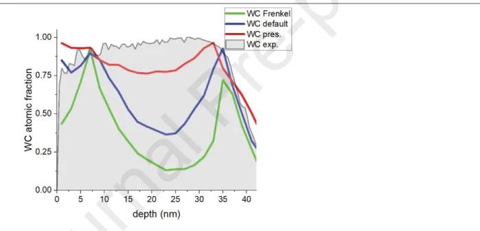
In the present case we have observed WC concentration close to 100%, thus in this case no limit in the formation of the tungsten carbide will be forced. It is clear, that in those rare cases, when there are unreacted W and C together, this model fails and overestimates the amount of tungsten carbide. Fig. 3 shows the comparison of the tungsten carbide distributions calculated from the C and W distributions shown in Fig. 2 with that of the measured AES depth profile.
Fig. 3. The WC distribution calculated from the C and W distributions shown in Fig. 2 and the one given by the experiment (AES depth profiling). The legends stand for calculated WC distribution by applying various relocation threshold energies as: WC Frenkel C 25 eV, W Frenkel 38 eV, WC default for all elements 8 eV, WC pres. for all elements 2 eV, WC exp.
experimentally determined distribution.
Using 2 eV relocation threshold energy for all elements produced a surprisingly good agreement between the simulation and experiment. Evidently this good agreement for a single case
alone does not justify our procedure. Therefore, in the following we will apply the same procedure for a series of measurements to check the validity of the method.
2.2.3. Comparison of the measured and calculated WC distributions
Both the measurement and simulation provide atomic fraction vs. depth curves. In comparing the curves one must be aware, however, that, as we have reported, the AES depth profiling introduces artefact [21]. Artefact production is most severe at the beginning of the intermixing process and with the formation of thicker WC layers it becomes milder. Thus, in those cases when only slight intermixing occurs, for the comparison with the experimental curve the simulated one will be “AES depth profiled”. For this procedure the simulated elemental distributions are the input for a TRIDYN simulation applying exactly same ion bombardment conditions, which are used in the depth profiling. In this TRYDIN simulation since the deposited energy is low (1keV Ar+ ions with grazing angle of incidence is used for depth profiling) the default parameters are used except the surface binding energy which is chosen to fit the experimentally determined relative sputtering yield.
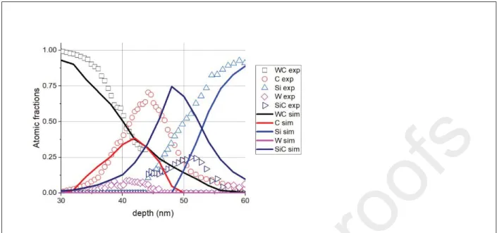
As it will be shown, we can fairly well predict the experimental results concerning the WC formation. All the studied samples are grown on Si substrate and the last layer is always made of C. The intermixing of C/Si system, however, occurs by ballistic mixing and can be well described by TRIDYN simulation, using parameters of ballistic mixing, which are vastly different from those used in this calculation [13]. Consequently, our simulation cannot describe the C/Si interface region, which is shown in Fig 4. Thus, this region, which in fact is unimportant from the point of view of WC formation, will be ignored in the following.
Fig. 4. The comparison of the measured and simulated depth profiles at the multilayer /sample interface region. Sample: C 10nm/W 24.5 nm / C 9.1 nm, ion irradiation: 40 keV Ar+, 3 x10¹⁶ ions/cm2. The legends: exp and sim stand for experimental and simulation, resp.
Summarizing the process of the calculation of the WC in-depth distributions for better understanding Fig. 5 shows a scheme of the simulation and calculation process.
Fig. 5. Scheme of the evaluation procedure
3. RESULTS AND DISCUSSION
WC formation was studied over a wide range of parameters; the projectile, projectile energy, fluence and sample structure have been varied. We will compare the experimentally measured WC distributions with the calculated ones for checking the validity of our procedure. It should be emphasized that in the calculations we have always used the same parameters and no fitting has been applied. The calculation provides two curves: the one given by the TRIDYN simulation (the real concentration distribution) and the one which was produced by “AES depth profiling” of the simulated distribution. This step is important for comparison of the simulated depth profile with the experimentally measured one. In the following we will report on four experiments together with the corresponding simulations to show how can one look for proper irradiation conditions and sample structure to produce a desired tungsten-carbide layer.
3.1 Ar+ irradiation of “thick” layers
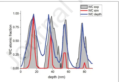
40 keV Ar+ irradiation was applied on sample with structure of C 15.8 nm /W 22.7 nm/C 17.2 nm/ W 24.3 nm/C 21.1 nm/ Si substrate. The fluence was 6 x 10¹⁵ ion/cm2. Here, because of the thick layers, we expect weak intermixing and thus the simulated and experimental distributions might strongly deviate; the results are shown in Fig. 6.
Fig. 6. The WC distribution obtained on sample with a structure of C 15.8 nm /W 22.7 nm/C 17.2 nm/ W 24.3 nm/C 21.1 nm/ Si substrate after ion irradiation, 40 keV Ar+ 6 x 10¹⁵.
The simulation shows that the WC production strongly decreases with the depth, which agrees with the expectations. At the first C/W and W/C interfaces there are slight degree of WC production, but on the following two interfaces WC can only be found in traces. On the other hand, the experiment shows substantial WC production on all interfaces (though continuous layer is not produced), the amount of the WC weakly depends on the depth; this strange behavior is due to the artefact production of the AES depth profiling. If we simulate the AES depth profile based on the distributions provided by the TRIDYN simulation, (Fig. 6, blue curve) excellent agreement with the measured curve has been found, except for the weaker fusion of the first and second WC distributions in the experiment than in the simulation. The small 2-4 nm shifts of the maximum is due to small error in the sputtering yield values (which determines the amount of the removed layer, that is, the depth) of the experiment and simulation.
3.2. Thinner layers higher fluence
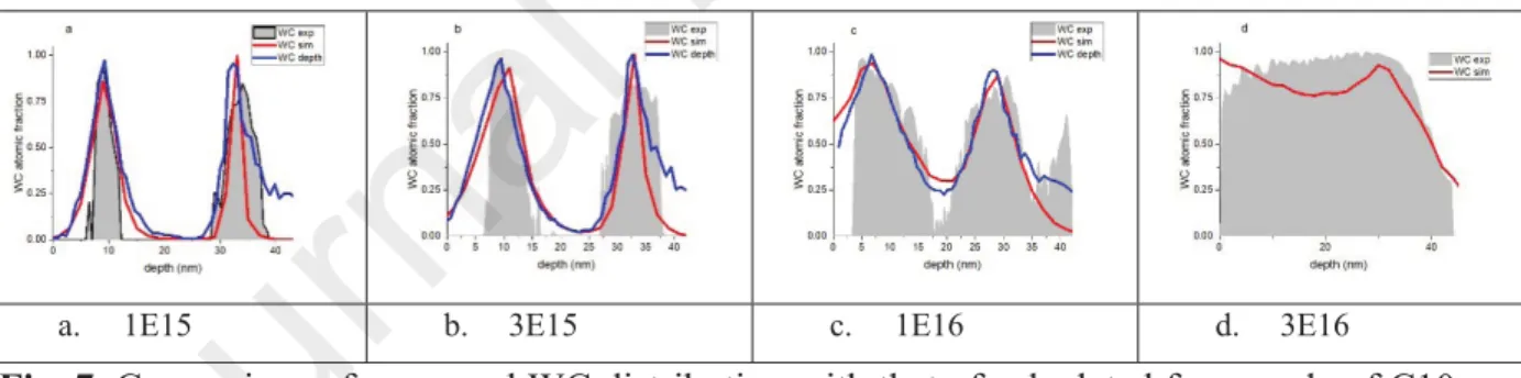
Fig. 7 shows the comparison of measurements and calculation for sample made of thinner layer that that the previous, which are C 10nm /W 24.5 nm / C 9.1 nm, after irradiation with 40 keV Ar+ with various fluences.
a. 1E15 b. 3E15 c. 1E16 d. 3E16
Fig. 7. Comparison of measured WC distribution with that of calculated for sample of C10nm /W 24.5 nm / C 9.1 nm, irradiated by 40 keV Ar+ applying various fluences.
The experimental results agree well with the expectations. The projected range of the 40 keV Ar+ in this sample is 21 ± 10 nm, which means that the deposited energy at the first interface is higher than that at the second one. Compound formation starts along interfaces and with increasing fluence the WC grows into the W layer, and at fluence of 3 x 10¹⁶ ion/cm2, a compact WC layer appears. At the beginning of the ion irradiation, at a fluence of 1 x 10¹⁵ ion/cm2, though
the deposited energy at the W/C is much less than that at the first C/W interface (see the projected range) the width of the WC layer seems to be wider than that of the first C/W interface. The calculated WC distributions, however, follow the expectation; the amount of WC is less in the second interface than in the first interface. On the other hand, simulating the depth profile, shown by the blue curve, surprisingly good agreement with the experiments is found, showing that at this slight intermixing the artefact due to the AES depth profiling really seriously corrupts the results.
At higher fluences artefact production is weaker and calculated and simulated profiles do not differ too much, and there is a good agreement with the measured profiles. It should be emphasized that the simulated AES depth profiles agree excellently with the measured AES depth profiles in a rather large, 1 x 10¹⁵ – 3 x 10¹³ ion/cm2, (factor if 30) fluence range. There are systematic differences as well. The onset of the experimentally measured first WC distribution at about 8 nm depth, especially at low fluences, is much steeper than that provided by the calculation. Similarly, the calculation predicts a somewhat faster fusion of the layers at low fluences (Fig. 7 b and c) than that observed in the experiments. Just contrary, in case of higher fluence, resulting in ″compact″ layer formation (Fig. 7 d), the calculation predicts slower fusion of the WC layers than that shown by the experiment. Nevertheless, these deviations do not affect the main picture; the total amount (integral) of the calculated and measured WC do not deviate more than 15 %. Anyhow with this choice a relatively good quality WC layer with a thickness of about 35 nm could be produced.
3.3. Energy and projectile dependence
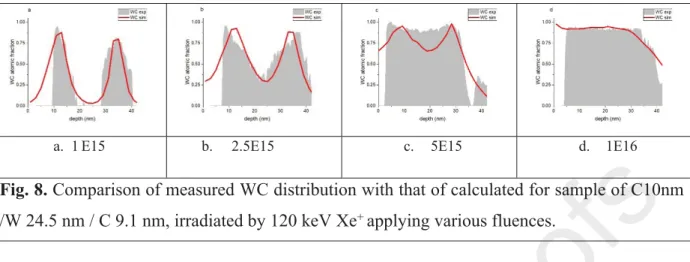
The same sample has been irradiated by applying a vastly different projectile, Xe+, and vastly different energy, 120 keV. Because of the higher atomic number projectile and energy, stronger intermixing and compound formation is expected. In this case WC distributions provided by the TRIDYN simulation will be compared with the experimentally determined ones since at the stronger intermixing the artefact due to the AES depth profiling becomes insignificant [21]. We emphasize again that for the TRIDYN simulation the same parameters have been used as previously, so no fitting has been applied. Fig. 8 shows the results.
a. 1E15 b. 2.5E15 c. 5E15 d. 1E16
Fig. 8. Comparison of measured WC distribution with that of calculated for sample of C10nm /W 24.5 nm / C 9.1 nm, irradiated by 120 keV Xe+ applying various fluences.
The experimental results agree with the expectations; stronger WC formation occurs using the same fluence and higher WC concentration at the deeper W/C interface than when using 40 keV Ar+. The agreement between WC distributions provided by the experiments and by TRIDYN simulations is very good again. The differences are exactly the same as in the case of Ar+ 40 keV irradiation, that is, the simulation fails at the beginning of the build-up of the WC distribution, and predicts a somewhat slower fusion (8.c) of the two (starting from the C/W and W/C interfaces) WC distributions. The tungsten-carbide produced is slightly better than the one made by Ar+, but the thickness is the same (it cannot be more since the whole amount of W has been transformed to carbide).
3.4. Making thicker carbide layer
If there is a need for thicker tungsten-carbide, then based on the above a different layer structure is to be chosen, like C 8 nm / W 18 nm / C 8.7 nm / W 18.6 nm / C 7.1 nm/ Si substrate.
This sample was subjected to Ar+ irradiation of 80 keV with fluences of 3E15 and 3E16, resp. The results are shown in Fig. 9.
a. 3E15 b. 3E16
Fig. 9. Comparison of measured WC distribution with that of calculated for sample of C 8 nm / W 18 nm / C 8.7 nm / W 18.6 nm / C 7.1 nm/ Si substrate, irradiated by 80 keV Ar+ applying various fluences.
The thickness of the tungsten carbide produced, using the C 8 nm / W 18 nm / C 8.7 nm / W 18.6 nm / C 7.1 nm/ Si substrate sample and applying 80 keV Ar+ ion bombardment with fluence of 3E16 ion/cm2 is larger than before; it is around 55 nm. The agreement between the simulations and experiments is reasonable good. Considering the tungsten-carbide formation at lower fluence we observe again serious artefact production; the profile provided by the AES depth profiling is strongly different from that provided the simulation. On the other hand, if we “AES depth profile”
the simulated distribution reasonable good agreement with the experimentally measured curve is found. This result emphasizes a./ our method describes well the artefact production b./ in AES depth profiling if this or similar material at lower mixing is applied one should always check the possible presence of the artefact.
Considering that the TRIDYN simulation, using the unusual 2 eV relocation threshold energies for all elements, describes the WC production surprisingly well over a wide range of ion energies, type of projectile and various initial sample structures, we can be sure that the physics of the intermixing is well represented by the TRIDYN simulation. It seems that the increased diffusivity (due to the decreased relocation threshold energy) is sufficient for producing higher intermixing -
which is expected based on the thermal spike model. The systematic deviations showed that the actual mixing process is a much richer phenomenon, but these additional processes could be more or less neglected from the point of view of layer formation.
4. CONCLUSIONS
Various C/W multilayer systems have been irradiated by Ar+ and Xe+ ions; the range of energies and fluences varied between 40-110 keV, and 0.07 - 6x10¹⁶ ions/cm2, respectively. The component in-depth distributions have been determined by AES depth profiling. All irradiation experiments have been simulated by TRIDYN code choosing 2eV relocation threshold energy and a simple rule for WC compound formation. Since the AES depth profiling might (depending on the distribution of components) produce artefact the simulated elemental distributions has been “AES depth profiled” for the comparison with experimentally found distributions. The simulated and measured depth distributions of WC agreed surprisingly well over a wide range of ion bombardment conditions and sample structures. This work also provides an example that the TRIDYN simulation can describe the ion mixing process even in systems in which the mixing is governed by thermal spike. These findings enable the design of WC-rich coatings which are known as protective layers.
AUTHOR INFORMATION
Corresponding Author
*E-mail: menyhard.miklos@ek-cer.hu
ACKNOWLEDGEMENT
The EU H2020 Project No. 824096 “RADIATE”, HZDR-Dresden and project funding of Centre for Energy Research is highly acknowledged. Authors thanks the support of VEKOP-2.3.3-15- 2016-00002 of the European Structural and Investment Funds. This paper was supported by the János Bolyai Research Scholarship of the Hungarian Academy of Sciences (Z. Fogarassy).
Guidance of N. Fairley in CasaXPS program is highly acknowledged. Thanks for A. Sulyok for providing AES facility. Thanks are given for L. Illés for FIB lamella preparation.
REFERENCES
[1] S. Gupta, D.C. Agarwal, S.A. Khan, S. Neeleshwar, S. Ojha, S. Srivastava, A. Tripathi, S.
Amirthapandian, B.K. Panigrahi, D.K. Avasthi, PbTe nanocrystal formation by interface mixing of Te/Pb bilayer using low energy ions, Mater. Sci. Eng. B. 184 (2014) 58–66.
https://doi.org/10.1016/j.mseb.2014.01.002.
[2] A. Arranz, C. Palacio, Ion beam mixing of Ti/Al interfaces by nitrogen irradiation, Surf.
Sci. 601 (2007) 4510–4514. https://doi.org/10.1016/j.susc.2007.04.172.
[3] R. Escobar Galindo, N. Benito, D. Duday, G.G. Fuentes, N. Valle, P. Herrero, L. Vergara, V. Joco, O. Sanchez, A. Arranz, C. Palacio, In-depth multi-technique characterization of chromium–silicon mixed oxides produced by reactive ion beam mixing of the Cr/Si interface, J. Anal. At. Spectrom. 27 (2012) 390. https://doi.org/10.1039/c2ja10296j.
[4] P. Sigmund, A. Gras-Marti, Theoretical aspects of atomic mixing by ion beams, Nucl.
Instrum. Methods. 182–183 (1981) 25–41. https://doi.org/10.1016/0029-554X(81)90668-6.
[5] Y.-T. Cheng, Thermodynamic and fractal geometric aspects of ion-solid interactions, Mater. Sci. Rep. 5 (1990) 45–97. https://doi.org/10.1016/S0920-2307(05)80007-6.
[6] W. Bolse, Mechanisms of ion beam induced atomic mixing in solids, Mater. Sci. Eng. A.
253 (1998) 194–201. https://doi.org/10.1016/S0921-5093(98)00727-8.
[7] J. Desimoni, A. Traverse, Model for compound formation during ion-beam mixing, Phys.
Rev. B. 48 (1993) 13266–13272. https://doi.org/10.1103/PhysRevB.48.13266.
[8] M.G. Stepanova, Effect of Ion Beam Mixing and Compound Formation on Sputter Depth Profile of a Ta/Si Multilayer Thin Film, Surf. Interface Anal. 24 (1996) 416–418.
https://doi.org/10.1002/(SICI)1096-9918(199606)24:6<416::AID-SIA125>3.0.CO;2-Z.
[9] Á. Barna, L. Kotis, J. Lábár, A. Sulyok, A.L. Tóth, M. Menyhárd, P. Panjan, Growing imbedded Ni 3 C-rich layer with sharp interfaces by means of ion beam mixing of C/Ni layers, J. Phys. Appl. Phys. 44 (2011) 125405. https://doi.org/10.1088/0022-
3727/44/12/125405.
[10] I.P. Jain, G. Agarwal, Ion beam induced surface and interface engineering, Surf. Sci. Rep.
66 (2011) 77–172. https://doi.org/10.1016/j.surfrep.2010.11.001.
[11] F. Harbsmeier, W. Bolse, A.-M. Flank, Ion beam induced solid state reaction in Si/C layer systems, Nucl. Instrum. Methods Phys. Res. Sect. B Beam Interact. Mater. At. 178 (2001) 214–219. https://doi.org/10.1016/S0168-583X(00)00461-4.
[12] A.S. Racz, Z. Kerner, A. Nemeth, P. Panjan, L. Peter, A. Sulyok, G. Vertesy, Z. Zolnai, M.
Menyhard, Corrosion Resistance of Nanosized Silicon Carbide-Rich Composite Coatings Produced by Noble Gas Ion Mixing, ACS Appl. Mater. Interfaces. 9 (2017) 44892–44899.
https://doi.org/10.1021/acsami.7b14236.
[13] A.S. Racz, M. Menyhard, Design of Corrosion Resistive SiC Nanolayers, ACS Appl.
Mater. Interfaces. 10 (2018) 22851–22856. https://doi.org/10.1021/acsami.8b06425.
[14] A.S. Racz, D. Zambo, G. Dobrik, I. Lukacs, Z. Zolnai, A. Nemeth, P. Panjan, A. Deak, G.
Battistig, M. Menyhard, Novel method for the production of SiC micro and nanopatterns, Surf. Coat. Technol. 372 (2019) 427–433. https://doi.org/10.1016/j.surfcoat.2019.05.061.
[15] A.S. Racz, D. Dworschak, M. Valtiner, M. Menyhard, Scratching resistance of SiC-rich nano-coatings produced by noble gas ion mixing, Surf. Coat. Technol. 386 (2020) 125475.
https://doi.org/10.1016/j.surfcoat.2020.125475.
[16] P. Petrik, A.S. Racz, M. Menyhard, Complementary physicochemical analysis by
ellipsometry and Auger spectroscopy of nano-sized protective coating layers, Appl. Surf.
Sci. 534 (2020) 147593. https://doi.org/10.1016/j.apsusc.2020.147593.
[17] G. Battistig, Z. Zolnai, A. Németh, P. Panjan, M. Menyhárd, Nanoscale SiC production by ballistic ion beam mixing of C/Si multilayer structures, J. Phys. Appl. Phys. 49 (2016) 185303. https://doi.org/10.1088/0022-3727/49/18/185303.
[18] J. Esteve, G. Zambrano, C. Rincon, E. Martinez, H. Galindo, P. Prieto, Mechanical and tribological properties of tungsten carbide sputtered coatings, Thin Solid Films. 373 (2000) 282–286. https://doi.org/10.1016/S0040-6090(00)01108-1.
[19] E.C. Weigert, M.P. Humbert, Z.J. Mellinger, Q. Ren, T.P. Beebe, L. Bao, J.G. Chen, Physical vapor deposition synthesis of tungsten monocarbide (WC) thin films on different carbon substrates, J. Vac. Sci. Technol. Vac. Surf. Films. 26 (2008) 23–28.
https://doi.org/10.1116/1.2806941.
[20] K.A. Beadle, R. Gupta, A. Mathew, J.G. Chen, B.G. Willis, Chemical vapor deposition of phase-rich WC thin films on silicon and carbon substrates, Thin Solid Films. 516 (2008) 3847–3854. https://doi.org/10.1016/j.tsf.2007.06.170.
[21] A.S. Racz, Z. Fogarassy, P. Panjan, M. Menyhard, Evaluation of AES depth profiles with serious artefacts in C/W multilayers, Appl. Surf. Sci. 582 (2022) 152385.
https://doi.org/10.1016/j.apsusc.2021.152385.
[22] Á. Barna, B. Pécz, M. Menyhard, TEM sample preparation by ion milling/amorphization, Micron. 30 (1999) 267–276. https://doi.org/10.1016/S0968-4328(99)00011-6.
[23] N. Fairley, A. Carrick, N. Fairley, Recipes for XPS data processing, Acolyte Science, Knutsford, 2005.
[24] K.D. Childs, C.L. Hedberg, Physical Electronics, Incorporation, eds., Handbook of Auger electron spectroscopy: a book of reference data for identification and interpretation in Auger electron spectroscopy, 3. ed, Physical Electronics, Eden Prairie, 1995.
[25] L. Zommer, A. Jablonski, L. Kotis, G. Safran, M. Menyhárd, Simulation and measurement of AES depth profiles; a case study of the C/Ta/C/Si system, Surf. Sci. 604 (2010) 633–
640. https://doi.org/10.1016/j.susc.2010.01.007.
[26] L. Kotis, M. Menyhard, A. Sulyok, G. Sáfrán, A. Zalar, J. Kovač, P. Panjan, Determination of the relative sputtering yield of carbon to tantalum by means of Auger electron
spectroscopy depth profiling, Surf. Interface Anal. 41 (2009) 799–803.
https://doi.org/10.1002/sia.3101.
[27] W. Möller, W. Eckstein, Ion mixing and recoil implantation simulations by means of tridyn, Nucl. Instrum. Methods Phys. Res. Sect. B Beam Interact. Mater. At. 7–8 (1985) 645–649.
https://doi.org/10.1016/0168-583X(85)90448-3.
CRediT author statement
A.S. Racz: Methodology, Investigation, Formal Analysis, Validation, Visualization, Writing – Original Draft, Review & Editing, Project administration, Funding acquisition, Z.Fogarassy :Investigation, Writing - Review & Editing U. Kentsch: Investigation P.Panjan: Investigation, M. Menyhard: Conceptualization, Methodology, Formal Analysis, Validation, Visualization, Writing - Original Draft, Review & Editing
HIGHLIGHTS
- Tungsten carbide-rich coating layers have been produced by irradiating various C/W multilayers by noble gases.
- Doing some parametrization the TRIDYN simulation was able to predict the in-depth distribution of the elements after ion irradiation.
- The produced amount of carbide has been calculated by applying a simple rule.
- The agreement between the experimental and simulated curves has been checked in variously irradiated (different layer structures, projectiles, energies, fluences) samples.
- TRIDYN simulation might be applied for estimation of concentration distribution due to thermal spike mixing.
Declaration of interests
The authors declare that they have no known competing financial interests or personal relationships that could have appeared to influence the work reported in this paper.
The authors declare the following financial interests/personal relationships which may be considered as potential competing interests: