A Novel UWB Monopole Antenna with
Reconfigurable Band Notch Characteristics Based on PIN Diodes
Yahieal Alnaiemy, and Lajos Nagy
A Novel UWB Monopole Antenna with
Reconfigurable Band Notch Characteristics Based on PIN Diodes
Yahieal Alnaiemy, and Lajos Nagy
Abstract—Our design for a novel UWB monopole antenna structure with reconfigurable band notch characteristics based on PIN diodes is presented in this paper. The proposed antenna is comprised of a modified circular patch and a partial ground plane. The band-notch characteristics are achieved by etching a slot on the partial ground plane and inserting three PIN diodes into the slots for adjusting the operating antenna bands. The reconfigurability is achieved by adding three PIN diodes to obtain eight states with UWB, dual and triple operating bands which can be obtained by changing the PIN state from ON to OFF, and vice versa. The proposed design shows a simple biasing process to switch the frequency bands with insignificant gain variation and low radiation efficiency reduction. The reconfigurability of the frequency is accomplished by adjusting the effective slot length through modifying the PIN diodes states at the desired operating bands. The desired operating frequency bands can be obtained by switching the diodes. A systematic parametric study based on a numerical analysis is invoked to verify and refine the proposed performance. The proposed antenna is fabricated on FR-4 substrate with dimensions of50×60×1mm3. The proposed antenna performance was tested experimentally and compared to the simulated results from CSTMW based on FIT. Experimental results were in concordance with simulated results. We found that the proposed antenna design had simple geometry and it was easy to control the frequency bands to suit the applications of WiMAX and WiFi systems.
Index Terms—UWB, Notch band, Reconfigurable antenna, PIN diode, Monopole antenna.
I. INTRODUCTION
D
UE to the rapid growth in wireless communication technology, multi-band antennas are highly valued. A significant drawback of conventional multi-band antennas is that they work only for specific operations. A new antenna with desired frequency specifications is required for each new application, increasing the relative cost. Reconfigurable antennas are usually based on active electronic devices to independently tune the required frequency, radiation, and polarization. They have come into urgent demand due to the growth in mobile communication technologies[1]. Reconfig- urable antennas have several advantages over conventional antennas such as smaller size, steerable radiation patterns, se- lecting the desired polarization for different frequency bands,Yahiea Alnaiemy is with Budapest University of Technology and Eco- nomics, Budapest, Hungary, and University of Diyala, College of Science e-mail: (yahiea@hvt.bme.hu).
Lajos Nagy is with the Budapest University of Technology and Economics, Department of Broadband Infocommunications and Electromagnetic Theory, Budapest, Hungary e-mail: (nagy.lajos@vik.bme.hu).
Manuscript received July 1, 2021; revised July 30, 2021.
and polarization, which reduces antenna system size and inter- symbol interference (ISI) impacts [2]. The integration of these configurations into a single antenna is a major challenge that researchers have been faced in recent years. Integrating antennas with modern high-speed semiconductors such as Positive Intrinisic Negative (PIN) diodes, Radio Frequency Microelectromechanical Systems (RF MEMS), and varactor diodes have been designed successfully for frequency, po- larization, and pattern tunability [3]-[25]. Due to the high- speed response and low forward resistance of PIN diodes, it was common practice to vary the antenna performance [3]
for direct antenna modulation (DAM) including Differential Phase Shift Keying (DPSK) modulation [4], which makes it more competitive for cognitive radio applications. A slotted patch antenna with two PIN diodes was presented by Majidet alfor frequency and pattern reconfiguration [5]. For antenna beam reconfiguration, a flexible antenna based on eight PIN diodes for wireless applications was introduced by Zhuet al in [6]. For frequency and pattern reconfiguration, an antenna based on two PIN diodes positioned within the slot etched in the front antenna patch was presented by Han et al in [7] for Long-Term Evolution (LTE). A reconfiguration of the antenna frequency and pattern was achieved using a printed antenna based on three Radio Frequency (RF) switches [8].
A reconfigurable Ultra-Wide-Band (UWB) filter antenna was featured in [9]; controlling operating frequency bands based on three PIN diodes that directly control the desired WLAN and WiMAX frequency bands. Wu et al in [10] introduced and designed a reconfigurable quad-band antenna based on Micro-Electomechanical-Systems (MEMS) switches. Control- ling operating frequency can be obtained by adjusting the MEMS switch, making it suitable for the cognitive radio base station. Hamidet alin [11] discussed and modelled a Vivaldi antenna by inserting four switchable ring slots within the antenna ground plane structure. The antenna reconfiguration may work in broadband or narrowband mode by changing the PIN diode switching facility. For single, multi-band, and UWB spectrum, a frequency reconfigurable microstrip antenna was presented by Yadavet alin [12], based on an array of 27 PIN diodes integrated into the partial ground structure. Yadavet al used many RF switches, increasing cost, manufacturing, and measurement difficulties relative to our antenna design. Tasouji et al in [13] presented a printed UWB slot antenna based on two PIN diodes with reconfigurable band-notch features that was mounted across the circular slot antenna patch to produce single and double band-notch characteristics. A UWB
A Novel UWB Monopole Antenna with
Reconfigurable Band Notch Characteristics Based on PIN Diodes
Yahieal Alnaiemy, and Lajos Nagy
Abstract—Our design for a novel UWB monopole antenna structure with reconfigurable band notch characteristics based on PIN diodes is presented in this paper. The proposed antenna is comprised of a modified circular patch and a partial ground plane. The band-notch characteristics are achieved by etching a slot on the partial ground plane and inserting three PIN diodes into the slots for adjusting the operating antenna bands. The reconfigurability is achieved by adding three PIN diodes to obtain eight states with UWB, dual and triple operating bands which can be obtained by changing the PIN state from ON to OFF, and vice versa. The proposed design shows a simple biasing process to switch the frequency bands with insignificant gain variation and low radiation efficiency reduction. The reconfigurability of the frequency is accomplished by adjusting the effective slot length through modifying the PIN diodes states at the desired operating bands. The desired operating frequency bands can be obtained by switching the diodes. A systematic parametric study based on a numerical analysis is invoked to verify and refine the proposed performance. The proposed antenna is fabricated on FR-4 substrate with dimensions of50×60×1mm3. The proposed antenna performance was tested experimentally and compared to the simulated results from CSTMW based on FIT. Experimental results were in concordance with simulated results. We found that the proposed antenna design had simple geometry and it was easy to control the frequency bands to suit the applications of WiMAX and WiFi systems.
Index Terms—UWB, Notch band, Reconfigurable antenna, PIN diode, Monopole antenna.
I. INTRODUCTION
D
UE to the rapid growth in wireless communication technology, multi-band antennas are highly valued. A significant drawback of conventional multi-band antennas is that they work only for specific operations. A new antenna with desired frequency specifications is required for each new application, increasing the relative cost. Reconfigurable antennas are usually based on active electronic devices to independently tune the required frequency, radiation, and polarization. They have come into urgent demand due to the growth in mobile communication technologies[1]. Reconfig- urable antennas have several advantages over conventional antennas such as smaller size, steerable radiation patterns, se- lecting the desired polarization for different frequency bands,Yahiea Alnaiemy is with Budapest University of Technology and Eco- nomics, Budapest, Hungary, and University of Diyala, College of Science e-mail: (yahiea@hvt.bme.hu).
Lajos Nagy is with the Budapest University of Technology and Economics, Department of Broadband Infocommunications and Electromagnetic Theory, Budapest, Hungary e-mail: (nagy.lajos@vik.bme.hu).
Manuscript received July 1, 2021; revised July 30, 2021.
and polarization, which reduces antenna system size and inter- symbol interference (ISI) impacts [2]. The integration of these configurations into a single antenna is a major challenge that researchers have been faced in recent years. Integrating antennas with modern high-speed semiconductors such as Positive Intrinisic Negative (PIN) diodes, Radio Frequency Microelectromechanical Systems (RF MEMS), and varactor diodes have been designed successfully for frequency, po- larization, and pattern tunability [3]-[25]. Due to the high- speed response and low forward resistance of PIN diodes, it was common practice to vary the antenna performance [3]
for direct antenna modulation (DAM) including Differential Phase Shift Keying (DPSK) modulation [4], which makes it more competitive for cognitive radio applications. A slotted patch antenna with two PIN diodes was presented by Majidet alfor frequency and pattern reconfiguration [5]. For antenna beam reconfiguration, a flexible antenna based on eight PIN diodes for wireless applications was introduced by Zhuet al in [6]. For frequency and pattern reconfiguration, an antenna based on two PIN diodes positioned within the slot etched in the front antenna patch was presented by Han et al in [7] for Long-Term Evolution (LTE). A reconfiguration of the antenna frequency and pattern was achieved using a printed antenna based on three Radio Frequency (RF) switches [8].
A reconfigurable Ultra-Wide-Band (UWB) filter antenna was featured in [9]; controlling operating frequency bands based on three PIN diodes that directly control the desired WLAN and WiMAX frequency bands. Wu et al in [10] introduced and designed a reconfigurable quad-band antenna based on Micro-Electomechanical-Systems (MEMS) switches. Control- ling operating frequency can be obtained by adjusting the MEMS switch, making it suitable for the cognitive radio base station. Hamidet alin [11] discussed and modelled a Vivaldi antenna by inserting four switchable ring slots within the antenna ground plane structure. The antenna reconfiguration may work in broadband or narrowband mode by changing the PIN diode switching facility. For single, multi-band, and UWB spectrum, a frequency reconfigurable microstrip antenna was presented by Yadavet alin [12], based on an array of 27 PIN diodes integrated into the partial ground structure. Yadavet al used many RF switches, increasing cost, manufacturing, and measurement difficulties relative to our antenna design. Tasouji et al in [13] presented a printed UWB slot antenna based on two PIN diodes with reconfigurable band-notch features that was mounted across the circular slot antenna patch to produce single and double band-notch characteristics. A UWB DOI: 10.36244/ICJ.2021.3.4
Yahiea Alnaiemy is with Budapest University of Technology and Eco- nomics, Budapest, Hungary, and University of Diyala, College of Science e-mail: (yahiea@hvt.bme.hu).
Lajos Nagy is with the Budapest University of Technology and Economics, Department of Broadband Infocommunications and Electromagnetic Theory, Budapest, Hungary e-mail: (nagy.lajos@vik.bme.hu).
Manuscript received July1, 2021; revised July 30, 2021.
A Novel UWB Monopole Antenna with Reconfigurable Band Notch Characteristics Based on PIN Diodes
JOURNAL OF LATEX CLASS FILES, VOL. 14, NO. 8, AUGUST 2015 2
monopole antenna with a reconfigurable band-notch based on two PIN diodes placed in antenna patch slots was presented by Hanet alin [14]. A reconfigurable microstrip slot antenna was presented by Oraiziet alin [15] through regulation the PIN diode embedded in the rectangular Split Ring Resonator (SRR). A reconfigurable UWB circular wide-slot antenna based on a stepped impedance resonator and an arc-shaped parasitic element was presented by Liet alin [16]. A notched- band UWB monopole antenna was introduced by Aghdam et alin [17] by connecting a varactor diode to a π-shaped patch. A reconfigurable cavity-backed slot antenna substrate integrated waveguide based on MEMS active elements was presented by Saghatiet alin [18]. A dual-band reconfigurable antenna based on a varactor diode lumped into the slot antenna was introduced by Behdad et al in [19]. A reconfigurable circular monopole based on Field Effect Transistor (FET) was presented in by Aboufoul et al in [20] for cognitive radio applications. A reconfigurable frequency band monopole with single and dual bands by employing three PIN diodes was presented by Shah et alin [21]. Nikolaou et al in [22]
controlled the frequency resonance by switching two PIN diodes soldered on both sides of an annular slot patch antenna.
Kimet alin [23] were proposed the polarization reconfigura- bility of a single feed circular patch antenna with five PIN diodes for low frequency and high frequency applications.
Elwi in [24] presented a reconfigurable antenna with remotely controlled by integrating a photo resistor array into a Hilbert patch antenna and adjusting the photo-resistors elimination for modern 5G applications. Singh et al in [25] were proposed a reconfigurable antenna for tuning the frequency bands in internet of things (IoT) systems using three PIN diodes. The researchers for wireless applications have presented several wideband monopole antennas. For instance, Reddy et al in [26] designed a flexible wideband monopole antenna for body-centric wireless communications. While, Mohandosset al in [27] designed a planar monopole fractal antenna to enhance the bandwidth for the personal wireless area and UWB applications. A multiband reconfigurable microwave filtering monopole antenna was presented by Kingslyet alin [28] based on switchable agile multiband filtenna for cognitive radios and Time Division Multiple Access (TDMA) systems.
Finally, compact wideband flexible planar monopole antennas were designed and analyzed for body-centric wireless and UWB communications [29].
The main objective of using such reconfigurable UWB fre- quency antenna is to overcome the overlap of the UWB with other bands, such as WiMAX bands. The antenna per- formances are obtained from a comparative study of the conventional antenna with the proposed antenna based on PIN diodes within the ground plane. This paper introduces a well-controlled operating frequency band based on three ON −OF F switch statues. By changing the slot length effectively through the PIN diode switching, a frequency band reconfiguration can be achieved at the desired operating bands accordingly. The proposed antenna shows a frequency band from 1.86GHzto 10.89GHzthat is significantly affected by PIN diodes switching. Eight cases, therefor, can be generated from switching the proposed three PIN diodes to provide
UWB, two, and/or three operating bands. The simulated re- sults are compared to the experimental results, which show acceptable agreement and confirm good performance of the proposed antenna. The obtained results, therefore, confirm that the proposed reconfigurable antenna is a better candidate for integration into wireless communication circuits.
II. ANTENNADESIGNDETIALS
The proposed antenna is designed to operate from 1.89 to 10.89 GHz to achieve a UWB with matching impedance in terms of S11 bellow -10dB according to the IEEE standard [15]. To be suitable for near and medium communication distance, the antenna’s peak realized gain should be within the range of 5.2dB-6.03dB for WiFi applications. The proposed antenna design, with the suggested parameters, is depicted in the next section. The antenna is modeled step by step to obtain a UWB response with an impedance bandwidth of (S11 < -10 dB) for the entire UWB (1.85-10.9)GHz.
Next, three PIN diodes are connected to the ground plane slot as switches to obtain eight PIN diode states. The main reason to choose three PIN diodes as switches is to change the proposed antenna’s effective electrical length to achieve frequency reconfigurability. By switching the state of the PIN diode between forward and backward, we can achieve the proposed antenna design to operate in UWB, dual, and triple- band mode.
III. METHODOLOGY OF THEANTENNADESIGN
In this section, we present the geometrical details of the proposed antenna to provide the design methodology for the optimal antenna performance. Next, antenna reconfiguration is discussed by switching the PIN diodes. The reconfigurability of the antenna can be accomplished by employing three PIN diodes as switches in the simulation setting to obtain dual-band mode, triple-band mode and UWB depending on the switch state. The authors have chosen a proposed monopole antenna, based on the circular shape and a defected ground structure that could expand the frequency band of operating as can be seen later in this paper.
A. UWB Monopole Antenna Design
The configuration of the proposed UWB monopole antenna geometry with the design parameters is illustrated in Fig. 1 and Table I, respectively. The proposed antenna is fabricated on a low-cost FR4 substrate with a r of 4.3, and a tanδ of 0.025. The proposed antenna size is 50mm×60mm with a substrate thickness of 1 mm. The modified circular patch is printed on the top side, and the defected partial ground plane is printed on the bottom side. The radiating patch and ground plane shapes are modified to achieve a UWB with good impedance matching.
In this section, reach the final antenna design is discussed.
The antenna design methodology was proposed by using a commercial software package of Computer Simulation Tech- nology Microwave Studio (CSTMW) with Finite Integration Technique (FIT) algorithm [30]. For this, the antenna band- width is monitored to get the best matching impedance over
JOURNAL OF LATEX CLASS FILES, VOL. 14, NO. 8, AUGUST 2015 3
Fig. 1. The proposed antenna geometry; (a) front view, (b) back view and (c) side view.
TABLE I
THEGEOMETRICAL DIMENSIONS OF THE PROPOSED ANTENNA:ALL DIMENSIONS INmm.
Parameter Dimension Parameter Dimension
L sub 60 L f 23
W sub 50 W f 1.65
L Grd 23 R 12
h sub 1 S 6
w 5 l 1
the entire band of interest by feeding the antenna with a 50 Ω port. To determine the influence of changing antenna dimensions, a parametric study was conducted. Antenna per- formance was monitored with respect to changingWf,W,l, S,h sub, andL Grdparameters representing feed line width, slot width of the partial ground plane, slot height of the partial ground plane, center-to-center distance, substrate height, and ground plane length, respectively. Next, a parametric study was applied to find the appropriate substrate type and size.
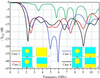
The antenna design begins with a conventional circular patch backed by a full ground plane as mentioned in case 1 (Fig.2).
Next, the ground plane is changed to a partial ground plane (without any slots) to improve the impedance matching, as mentioned in case 2. Next, the rectangular slot is etched from the ground plane to improve the proposed antenna bandwidth.
The frequency reconfiguration is accomplished by modifying the parasitic element electrically through switching the PIN diodes with the ground plane. The defected ground plane is made by integrating the PIN diodes without changing the UWB antenna performance. We observed that the desired UWB results are not obtained for the proposed antenna with partial ground plane, therefore, a slot is inserted within the partial ground plane to improve the bandwidth and the match- ing impedance. We observed that the antenna bandwidth of 3.5GHz to 9.5 GHz was obtained as mentioned in case 3.
A further modification of the proposed antenna is to involve a circular patch as denoted in case 4 of Fig. 2. The modification in this design includes another circular shape to generate a new frequency band. This modification in the radiator patch obtains a better impedance matching over the entire UWB and enhances the reference antenna bandwidth as shown in case 4.
We observed a very wide bandwidth (S11 <-10dB) of 1.85 GHz to 11GHz.
It is indicated from theS11spectra Fig. 2 that variation in
Fig. 2. Comparison of simulated|S11|spectra for four model cases.
the ground plane has significant effects on the antenna band- width. For example, the proposed antenna with full ground plane in case 1 shows narrow bandwidth around multiple frequency bands. Antenna bandwidth, therefore, is enhanced when a partial ground plane is modified. However, the antenna bandwidth is enhanced furthermore in cases 3 and 4 when the slot is introduced to the ground plane. The results are in agreement with the suggested antenna design’s requirements which are provided in Section II for achieving a wide-band with matching impedance below -10dB.
To maximize the antenna bandwidth further, the antenna feed line was connected to the Sub Miniature version A connector (SMA) center pin with a width ofWf. The feed line width is parametrically optimized as shown in Fig.3. It is indicated that varyingWf shows a major impact on the antenna bandwidth [24]. This study may lead to the best impedance matching and subsequently, a gradual bandwidth increase in the proposed antenna. Figure 3 shows the optimized results ofWf at 1.65 mmwith broader bandwidth over the frequencies from 1.85 GHz to 10.89GHz. This parametric study considersS11 < -10 dB impedance bandwidth for the entire UWB by changing Wf given the antenna wide band from 1.85 to 10.85 GHz.
The main purpose of the rectangular slot on the ground plane is to disturb the surface current to operate the antenna at lower frequency bands. The effects of changing the slot width (W) on the|S11|spectra (Fig. 4) was studied to realize the best matching impedance. We found that decreasing the slot width (W <5mm) causes impedance matching reduction from 2.5GHzto 7.8GHz in the low-frequency band, while an increase in slot width (W > 5 mm) creates problems with impedance matching from 7.2 GHz to 7.8GHz in the high-frequency band. The maximum impedance bandwidth and best impedance matching can be obtained when W = 5 mm. A sweep of the parameter W to achieve the proposed antenna work with a UWB mode with impedance bandwidth less than -10dB from 1.85GHz to 10.9GHz.
To maximize the antenna bandwidth, the height of the slot
monopole antenna with a reconfigurable band-notch based on two PIN diodes placed in antenna patch slots was presented by Hanet alin [14]. A reconfigurable microstrip slot antenna was presented by Oraiziet al in [15] through regulation the PIN diode embedded in the rectangular Split Ring Resonator (SRR). A reconfigurable UWB circular wide-slot antenna based on a stepped impedance resonator and an arc-shaped parasitic element was presented by Liet alin [16]. A notched- band UWB monopole antenna was introduced by Aghdam et al in [17] by connecting a varactor diode to a π-shaped patch. A reconfigurable cavity-backed slot antenna substrate integrated waveguide based on MEMS active elements was presented by Saghatiet alin [18]. A dual-band reconfigurable antenna based on a varactor diode lumped into the slot antenna was introduced by Behdad et al in [19]. A reconfigurable circular monopole based on Field Effect Transistor (FET) was presented in by Aboufoul et al in [20] for cognitive radio applications. A reconfigurable frequency band monopole with single and dual bands by employing three PIN diodes was presented by Shah et al in [21]. Nikolaouet al in [22]
controlled the frequency resonance by switching two PIN diodes soldered on both sides of an annular slot patch antenna.
Kimet alin [23] were proposed the polarization reconfigura- bility of a single feed circular patch antenna with five PIN diodes for low frequency and high frequency applications.
Elwi in [24] presented a reconfigurable antenna with remotely controlled by integrating a photo resistor array into a Hilbert patch antenna and adjusting the photo-resistors elimination for modern 5G applications. Singh et al in [25] were proposed a reconfigurable antenna for tuning the frequency bands in internet of things (IoT) systems using three PIN diodes. The researchers for wireless applications have presented several wideband monopole antennas. For instance, Reddy et al in [26] designed a flexible wideband monopole antenna for body-centric wireless communications. While, Mohandosset al in [27] designed a planar monopole fractal antenna to enhance the bandwidth for the personal wireless area and UWB applications. A multiband reconfigurable microwave filtering monopole antenna was presented by Kingslyet alin [28] based on switchable agile multiband filtenna for cognitive radios and Time Division Multiple Access (TDMA) systems.
Finally, compact wideband flexible planar monopole antennas were designed and analyzed for body-centric wireless and UWB communications [29].
The main objective of using such reconfigurable UWB fre- quency antenna is to overcome the overlap of the UWB with other bands, such as WiMAX bands. The antenna per- formances are obtained from a comparative study of the conventional antenna with the proposed antenna based on PIN diodes within the ground plane. This paper introduces a well-controlled operating frequency band based on three ON − OF F switch statues. By changing the slot length effectively through the PIN diode switching, a frequency band reconfiguration can be achieved at the desired operating bands accordingly. The proposed antenna shows a frequency band from 1.86GHzto 10.89GHzthat is significantly affected by PIN diodes switching. Eight cases, therefor, can be generated from switching the proposed three PIN diodes to provide
UWB, two, and/or three operating bands. The simulated re- sults are compared to the experimental results, which show acceptable agreement and confirm good performance of the proposed antenna. The obtained results, therefore, confirm that the proposed reconfigurable antenna is a better candidate for integration into wireless communication circuits.
II. ANTENNADESIGNDETIALS
The proposed antenna is designed to operate from 1.89 to 10.89 GHz to achieve a UWB with matching impedance in terms of S11 bellow -10dB according to the IEEE standard [15]. To be suitable for near and medium communication distance, the antenna’s peak realized gain should be within the range of 5.2dB-6.03dB for WiFi applications. The proposed antenna design, with the suggested parameters, is depicted in the next section. The antenna is modeled step by step to obtain a UWB response with an impedance bandwidth of (S11 < -10 dB) for the entire UWB (1.85-10.9)GHz.
Next, three PIN diodes are connected to the ground plane slot as switches to obtain eight PIN diode states. The main reason to choose three PIN diodes as switches is to change the proposed antenna’s effective electrical length to achieve frequency reconfigurability. By switching the state of the PIN diode between forward and backward, we can achieve the proposed antenna design to operate in UWB, dual, and triple- band mode.
III. METHODOLOGY OF THEANTENNADESIGN
In this section, we present the geometrical details of the proposed antenna to provide the design methodology for the optimal antenna performance. Next, antenna reconfiguration is discussed by switching the PIN diodes. The reconfigurability of the antenna can be accomplished by employing three PIN diodes as switches in the simulation setting to obtain dual-band mode, triple-band mode and UWB depending on the switch state. The authors have chosen a proposed monopole antenna, based on the circular shape and a defected ground structure that could expand the frequency band of operating as can be seen later in this paper.
A. UWB Monopole Antenna Design
The configuration of the proposed UWB monopole antenna geometry with the design parameters is illustrated in Fig. 1 and Table I, respectively. The proposed antenna is fabricated on a low-cost FR4 substrate with a r of 4.3, and a tanδ of 0.025. The proposed antenna size is 50mm×60mm with a substrate thickness of 1 mm. The modified circular patch is printed on the top side, and the defected partial ground plane is printed on the bottom side. The radiating patch and ground plane shapes are modified to achieve a UWB with good impedance matching.
In this section, reach the final antenna design is discussed.
The antenna design methodology was proposed by using a commercial software package of Computer Simulation Tech- nology Microwave Studio (CSTMW) with Finite Integration Technique (FIT) algorithm [30]. For this, the antenna band- width is monitored to get the best matching impedance over
Fig. 1. The proposed antenna geometry; (a) front view, (b) back view and (c) side view.
TABLE I
THEGEOMETRICAL DIMENSIONS OF THE PROPOSED ANTENNA:ALL DIMENSIONS INmm.
Parameter Dimension Parameter Dimension
L sub 60 L f 23
W sub 50 W f 1.65
L Grd 23 R 12
h sub 1 S 6
w 5 l 1
the entire band of interest by feeding the antenna with a 50 Ω port. To determine the influence of changing antenna dimensions, a parametric study was conducted. Antenna per- formance was monitored with respect to changingWf,W,l, S,h sub, andL Grdparameters representing feed line width, slot width of the partial ground plane, slot height of the partial ground plane, center-to-center distance, substrate height, and ground plane length, respectively. Next, a parametric study was applied to find the appropriate substrate type and size.
The antenna design begins with a conventional circular patch backed by a full ground plane as mentioned in case 1 (Fig.2).
Next, the ground plane is changed to a partial ground plane (without any slots) to improve the impedance matching, as mentioned in case 2. Next, the rectangular slot is etched from the ground plane to improve the proposed antenna bandwidth.
The frequency reconfiguration is accomplished by modifying the parasitic element electrically through switching the PIN diodes with the ground plane. The defected ground plane is made by integrating the PIN diodes without changing the UWB antenna performance. We observed that the desired UWB results are not obtained for the proposed antenna with partial ground plane, therefore, a slot is inserted within the partial ground plane to improve the bandwidth and the match- ing impedance. We observed that the antenna bandwidth of 3.5GHz to 9.5GHz was obtained as mentioned in case 3.
A further modification of the proposed antenna is to involve a circular patch as denoted in case 4 of Fig. 2. The modification in this design includes another circular shape to generate a new frequency band. This modification in the radiator patch obtains a better impedance matching over the entire UWB and enhances the reference antenna bandwidth as shown in case 4.
We observed a very wide bandwidth (S11 <-10dB) of 1.85 GHz to 11GHz.
It is indicated from theS11 spectra Fig. 2 that variation in
Fig. 2. Comparison of simulated|S11|spectra for four model cases.
the ground plane has significant effects on the antenna band- width. For example, the proposed antenna with full ground plane in case 1 shows narrow bandwidth around multiple frequency bands. Antenna bandwidth, therefore, is enhanced when a partial ground plane is modified. However, the antenna bandwidth is enhanced furthermore in cases 3 and 4 when the slot is introduced to the ground plane. The results are in agreement with the suggested antenna design’s requirements which are provided in Section II for achieving a wide-band with matching impedance below -10dB.
To maximize the antenna bandwidth further, the antenna feed line was connected to the Sub Miniature version A connector (SMA) center pin with a width ofWf. The feed line width is parametrically optimized as shown in Fig.3. It is indicated that varyingWf shows a major impact on the antenna bandwidth [24]. This study may lead to the best impedance matching and subsequently, a gradual bandwidth increase in the proposed antenna. Figure 3 shows the optimized results ofWf at 1.65 mmwith broader bandwidth over the frequencies from 1.85 GHz to 10.89GHz. This parametric study considersS11 <
-10 dB impedance bandwidth for the entire UWB by changing Wf given the antenna wide band from 1.85 to 10.85 GHz.
The main purpose of the rectangular slot on the ground plane is to disturb the surface current to operate the antenna at lower frequency bands. The effects of changing the slot width (W) on the|S11|spectra (Fig. 4) was studied to realize the best matching impedance. We found that decreasing the slot width (W <5mm) causes impedance matching reduction from 2.5GHz to 7.8GHzin the low-frequency band, while an increase in slot width (W > 5 mm) creates problems with impedance matching from 7.2GHz to 7.8GHz in the high-frequency band. The maximum impedance bandwidth and best impedance matching can be obtained when W = 5 mm. A sweep of the parameter W to achieve the proposed antenna work with a UWB mode with impedance bandwidth less than -10dB from 1.85GHz to 10.9GHz.
To maximize the antenna bandwidth, the height of the slot
A Novel UWB Monopole Antenna with Reconfigurable Band Notch Characteristics Based on PIN Diodes
JOURNAL OF LATEX CLASS FILES, VOL. 14, NO. 8, AUGUST 2015 4
Fig. 3. Effects of changing(Wf)on the|S11|spectra
Fig. 4. Effects of changingW on the|S11|spectra
on the partial ground plane has a pivotal function. However, We studied the effect of the slot height of the partial ground plane given by (l) on the proposed antenna performances. The effect on bandwidth for different ground plane slot heights is shown in Fig. 5.
As shown in Fig. 5, the narrower slot height (l= 0.5mm) indicates poor return loss at the 2.9GHz to 3.2GHz band.
Increasing the slot height (l > 1 mm) leads to enhanced
|S11|at the lower band (1.75-6.75)GHz, but poor impedance matching is found between 6.75GHzand 8.5GHz. However, the optimum ground slot height (l= 1 mm) provides the necessary impedance matching over the required frequency range, and the UWB width of the antenna is from 1.75 to 11GHz. These results were extremely close to the planned antenna specification, as shown in Section II. The length of partial ground plane (L Grd) shows a slight effect on the proposed antenna bandwidth. TheL Grdwas swept from 20 mmup to 25mmwith a step of 1mmto obtain the desired UWB frequency band. We observed from Fig. 6 that the
Fig. 5. Effects of changinglon the|S11|spectra
Fig. 6. Effects of changingL Grdon the|S11|spectra
proposed antenna operates as a UWB antenna whenL Grd= 23 mm. However, |S11| is improved dramatically when the ground plane length is gradually reduced. As a result, the required antenna design criteria are met by selecting L Grd
= 23mmfor the entire UWB mode with the best bandwidth impedance matching less than -10dB.
Figure 7 shows the circular patch development through five stages to illustrate the effects of changingSvalue from 0mm to 8mmwith a step of 2mm. The parameterSrepresents a center-to-center distance between two circular patches ( Fig.1).
In this design step, the simulated|S11|spectra of the proposed antenna with a different value ofS is illustrated in Fig. 7.
At a low value of S (S< 6 mm), the antenna does not provide a UWB impedance bandwidth. The proposed antenna shows poor matching impedance in the high- frequency band from 7.2 GHz to 8.1 GHz. Increasing S above 6 mm, improves the impedance bandwidth. However, the antenna still suffers from a matching impedance problem at the frequencies from 7.3 GHz to 8.3 GHz. The distribution of the surface
JOURNAL OF LATEX CLASS FILES, VOL. 14, NO. 8, AUGUST 2015 5
Fig. 7. Simulated|S11|spectra for the proposed patches.
Fig. 8. Effects of changingh subon the|S11|spectra.
current of the proposed antenna with S = 6 mm is mainly extended. By consideringS= 6mm, therefore, the impedance matching bandwidth is significantly enhanced to suit the proposed antenna requirement to work with UWB mode.
Figure 8 demonstrates the effects of changing the substrate thickness on the |S11| spectra. The substrate thickness was changed according to the available commercial resources :0.26, 1, and 1.6mm. Based on the|S11|spectra, the proposed antenna shows a wider impedance bandwidth for h sub = 1.6mmbut cannot support the desired UWB. The proposed antenna depicts a wide impedance bandwidth only when it has substrate thickness of 1mm. As a result, ifh sub= 1mm, the proposed antenna operates in UWB mode with a matching impedance of less than -10dB from 1.85 to 10.9GHz.
Additionally, we discuss the effects of substrate type change on antenna performance. As shown in Fig. 9, FR-4 substrate with r= 4.3 and tanδ =0.025 covers a wider bandwidth compared to other substrates in this study, which satisfied the entire UWB.
Fig. 9. Effects of changing substrate materials on the|S11|spectra.
Fig. 10. Effects of substrate size on the|S11|spectra.
Regarding substrate size, we adjusted the proposed antenna dimensions within five different dimensions. As shown in Fig. 10, we found the best antenna dimensions are 50 mm×60 mm, which satisfied the entire UWB.
B. Reconfigurable UWB Monopole Antenna
The reconfiguration of the proposed antenna, which has a slot on the ground plane, is shown in Fig.11(a). The slot on the ground plane is mounted by a narrow a metal strip with dimension 0.5mm×4mmto provide independent DC biasing for PIN diodes as shown Fig.11(a). The frequency configuration is changed by adjusting three PIN diodes con- nected to the ground plane slot. In the RF domain, PIN diodes are commonly used, therefore, the PIN diode RF resistance is connected to the DC bias current and can be used as an RF switch. When the diode is positively biased, the short circuit is turned on, and the open circuit is turned ON when it is reverse biased. Usually, the diode resistance
Fig. 3. Effects of changing(Wf)on the|S11|spectra
Fig. 4. Effects of changingW on the|S11|spectra
on the partial ground plane has a pivotal function. However, We studied the effect of the slot height of the partial ground plane given by (l) on the proposed antenna performances. The effect on bandwidth for different ground plane slot heights is shown in Fig. 5.
As shown in Fig. 5, the narrower slot height (l= 0.5mm) indicates poor return loss at the 2.9GHz to 3.2GHz band.
Increasing the slot height (l > 1 mm) leads to enhanced
|S11|at the lower band (1.75-6.75)GHz, but poor impedance matching is found between 6.75GHzand 8.5GHz. However, the optimum ground slot height (l= 1 mm) provides the necessary impedance matching over the required frequency range, and the UWB width of the antenna is from 1.75 to 11 GHz. These results were extremely close to the planned antenna specification, as shown in Section II. The length of partial ground plane (L Grd) shows a slight effect on the proposed antenna bandwidth. TheL Grdwas swept from 20 mmup to 25mmwith a step of 1mmto obtain the desired UWB frequency band. We observed from Fig. 6 that the
Fig. 5. Effects of changinglon the|S11|spectra
Fig. 6. Effects of changingL Grdon the|S11|spectra
proposed antenna operates as a UWB antenna whenL Grd= 23 mm. However, |S11| is improved dramatically when the ground plane length is gradually reduced. As a result, the required antenna design criteria are met by selecting L Grd
= 23mmfor the entire UWB mode with the best bandwidth impedance matching less than -10dB.
Figure 7 shows the circular patch development through five stages to illustrate the effects of changingSvalue from 0mm to 8mmwith a step of 2mm. The parameterSrepresents a center-to-center distance between two circular patches ( Fig.1).
In this design step, the simulated|S11|spectra of the proposed antenna with a different value ofSis illustrated in Fig. 7.
At a low value of S (S< 6 mm), the antenna does not provide a UWB impedance bandwidth. The proposed antenna shows poor matching impedance in the high- frequency band from 7.2 GHz to 8.1 GHz. Increasing S above 6 mm, improves the impedance bandwidth. However, the antenna still suffers from a matching impedance problem at the frequencies from 7.3 GHz to 8.3 GHz. The distribution of the surface
Fig. 7. Simulated|S11|spectra for the proposed patches.
Fig. 8. Effects of changingh subon the|S11|spectra.
current of the proposed antenna with S = 6 mm is mainly extended. By consideringS= 6mm, therefore, the impedance matching bandwidth is significantly enhanced to suit the proposed antenna requirement to work with UWB mode.
Figure 8 demonstrates the effects of changing the substrate thickness on the |S11| spectra. The substrate thickness was changed according to the available commercial resources :0.26, 1, and 1.6mm. Based on the|S11|spectra, the proposed antenna shows a wider impedance bandwidth for h sub = 1.6mmbut cannot support the desired UWB. The proposed antenna depicts a wide impedance bandwidth only when it has substrate thickness of 1mm. As a result, ifh sub= 1mm, the proposed antenna operates in UWB mode with a matching impedance of less than -10 dBfrom 1.85 to 10.9GHz.
Additionally, we discuss the effects of substrate type change on antenna performance. As shown in Fig. 9, FR-4 substrate with r= 4.3 and tanδ =0.025 covers a wider bandwidth compared to other substrates in this study, which satisfied the entire UWB.
Fig. 9. Effects of changing substrate materials on the|S11|spectra.
Fig. 10. Effects of substrate size on the|S11|spectra.
Regarding substrate size, we adjusted the proposed antenna dimensions within five different dimensions. As shown in Fig.
10, we found the best antenna dimensions are 50 mm×60 mm, which satisfied the entire UWB.
B. Reconfigurable UWB Monopole Antenna
The reconfiguration of the proposed antenna, which has a slot on the ground plane, is shown in Fig.11(a). The slot on the ground plane is mounted by a narrow a metal strip with dimension0.5 mm×4 mmto provide independent DC biasing for PIN diodes as shown Fig.11(a). The frequency configuration is changed by adjusting three PIN diodes con- nected to the ground plane slot. In the RF domain, PIN diodes are commonly used, therefore, the PIN diode RF resistance is connected to the DC bias current and can be used as an RF switch. When the diode is positively biased, the short circuit is turned on, and the open circuit is turned ON when it is reverse biased. Usually, the diode resistance
A Novel UWB Monopole Antenna with Reconfigurable Band Notch Characteristics Based on PIN Diodes
JOURNAL OF LATEX CLASS FILES, VOL. 14, NO. 8, AUGUST 2015 6
can vary from 10 kΩ to less than 1Ω by controlling its bias current [32]. In UWB mode, switching the PIN diodes may dramatically affect the impedance matching that reduces the bandwidth due to parasitic inductance, capacitance, and resistance. Nevertheless, the DC biasing circuit is necessary to control the RF signal flow to the antenna structure. For this, integrating the PIN diodes into the ground plane has minimum effect compared with maximum loading effects on the antenna performance when the PIN diodes are integrated within the radiating patch [31]. We prefer to mount the PIN diodes and associate the biasing circuit in the ground plane instead of the patch antenna due to the biasing complexity and the antenna radiation interfering with the antenna structure [31]. The main reason for choosing three PIN diodes as switches is to change the proposed antenna effective electrical length to achieve the proposed frequency reconfigurability. The defected partial ground plane resonators self-resonance frequencies depend on their physical dimensions. The defected partial ground plane operation is very similar to a circuit with parallel inductance capacitance [8]. Through an increase in the overall length of the ground plane slot, the inductance could be raised, while reducing the slot width increases the capacitance. The notched band frequency can be approximated using equation 1 [32].
fnotch= c
4(L√e) (1)
Here, the overall length of the defected partial ground plane slot is L, e is the effective dielectric constant, and c is the light speed in the free space.
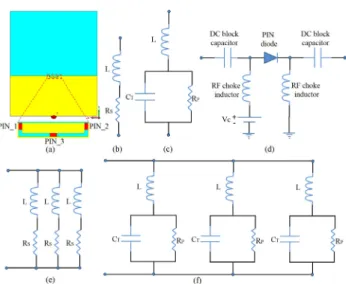
In the proposed configuration, the slot width (W) and slot length (l) are fixed to 5 mm and 1 mm, respectively. The resonant frequency can be controlled using the overall defected partial ground plane slot length through the PIN diodes. The proposed antenna depicts a dual and triple notch band only when the PIN diodes are inserted within the ground plane slot. The three PIN diodes are used to adjust inductance and capacitance of the antenna equivalent circuit. This variation contributes to the tuning of impedance matching in desired operating bands and optimizing the corresponding resonant circuitry. Figure 11(b, c, e, and d) indicates the equivalent circuits for the ON and OFF conditions.
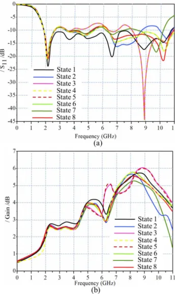
To explain the PIN diode operation (ON-OFF), an ideal PIN diode is used as a switch in the simulation, and the proposed diodes are modelled as a metal strip only for direct open and short states. Under ON status, the respective circuit shows that the inductor (L) and a resistor (RS) are loaded in series connections, while an inductor (L) is loaded in series with a capacitor (CT) when the PIN is switched to OFF. In this analysis we used a suitable bias to prevent the coupling of the RF signal and the bias current [31]. Capacitors are utilized to block DC and pass RF signal. Inductors are used as chokes to block RF signal and pass DC as seen in Fig.11(d). We ob- served that it is possible to switch the proposed reconfigurable antenna between a UWB mode, dual band-notch modes and a triple band-notch mode. Figure 12 presents the|S11|spectra and the realized gain versus frequency of the proposed antenna based on the eight diode states. State 1 is establishing the UWB (1.86-10.89) GHz when all the PIN diodes are OFF.
Fig. 11. The proposed PIN diodes and bias circuit (a) proposed reconfugrable antenna, (b) equivalent circuit for ON state of one PIN diode, (c) equivalent circuit for OFF state of one PIN diode, (d) bias circuit for PIN diodes, (e) equivalent circuit for ON state of all PIN diodes, and (e) equivalent circuit for OFF state of all PIN diodes,.
States 4, 6, and 8 establish the dual bands, and states 2, 3, 5, and 7 are solely responsible for obtaining the triple bands. The transition between dual, triple and UWB can be explained by the change in the surface current. Indeed, the electrical length of the proposed antenna structure is really determined by the diodes condition (ON and OFF). From the proposed antenna
|S11|, the antenna bandwidths are significantly affected by the PIN diode switching. It can be inferred that the parasitic element affects the antenna bandwidth to be changed from the UWB to the narrow bands. Due to parasitic effects, the proposed UWB mode is decreased to narrowband mode. The bandwidth is changed from UWB to narrow band due to the difference in surface current distribution [16]. In fact, the proposed antenna electrical length can be determined from switching PIN diodes conditions as summarized in Table II.
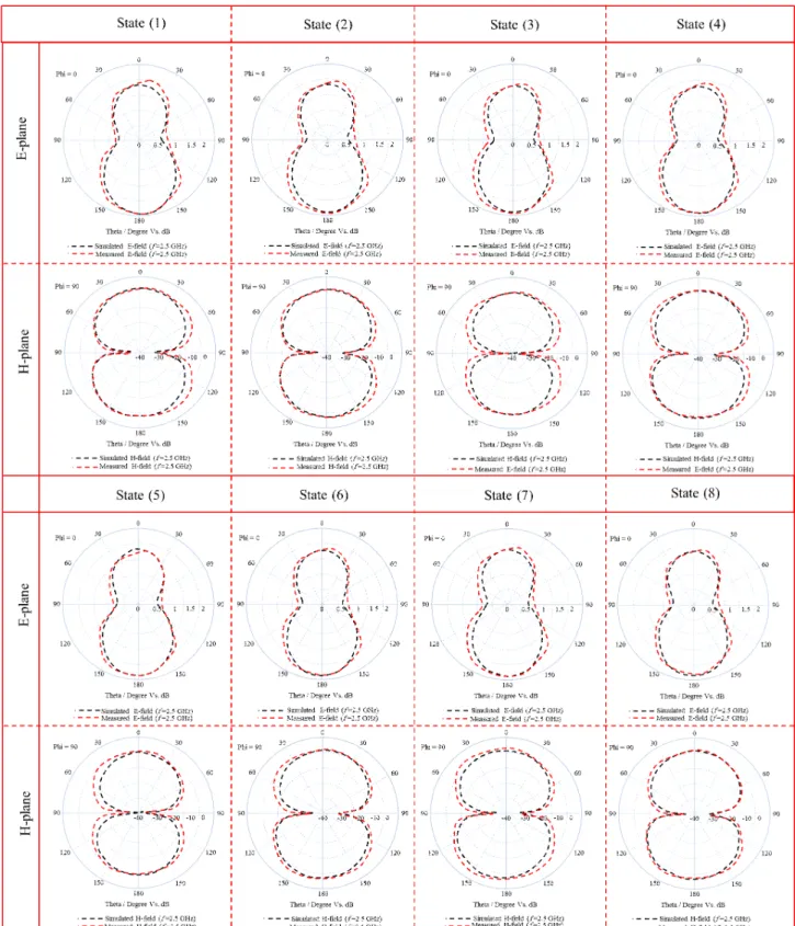
We observed from the realized antenna gain versus frequency plot in which frequencies the UWB notch antenna radiates and where it does not. The obtained gain is found to be suitable for short and medium wireless applications [7]; ranging from 5.2dB to 6.1dB as shown in Fig. 12(b).
TABLE II
SUMMARY OF THEPINDIODES SWITCHING STATES MODES
State PIN 1 PIN 2 PIN 3 Operation (GHz) Peak Realized Gain (dB)
1 OFF OFF OFF UWB (1.86-10.89) 5.7
2 OFF OFF ON three notch (2.7-3.47), (5.45-6.4) and (8.87-10.05) 5.65 3 OFF ON OFF three notch (2.76-3.53), (3.9-6.4), and (7.16-8.05) 6
4 OFF ON ON two notch (2.7-3.5) and (5.43-6.44) 5.79
5 ON OFF OFF three notch (2.76-3.53), (3.9-6.4), and (7.16-8.05) 6.03
6 ON OFF ON two notch (2.7-3.5) and (5.43-6.44) 5.78
7 ON ON OFF three notch (2.74-3.4), (5.44-6.38) and (7.54-8.4) 5.2
8 ON ON ON three notch (2.7-3.5) and (5.4-6.46) 5.5
IV. FABRICATION, MEASUREMENTS,ANDTESTING
The proposed antenna is fabricated calculating the optimal design. The fabrication is performed in the printed wiring board laboratory of the BME-ETT, Department of Electronic
JOURNAL OF LATEX CLASS FILES, VOL. 14, NO. 8, AUGUST 2015 7
Fig. 12. Simulated (a) reflection coefficient Vs frequency, and (b) realized gain Vs frequency for the all the PIN diodes states.
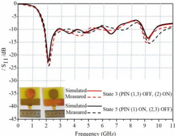
Technology, Budapest University of Technology and Eco- nomics. The Printed Circuit Board (PCB) technique is used to fabricate the proposed antenna on low-cost FR-4 substrate with a dielectric constant of 4.3, a loss tangent of 0.025, and substrate thickness of 1mm. The fabricated antenna is fed through an SMA connector. BAR6303W PIN diodes are uti- lized as high-speed RF-signal switches [33]. Different shapes of the slotted ground plane connect to the PIN diodes. Four re- configurable antennas are fabricated based on the information presented in Fig. 1. To identify the characteristics of the band notch, the PIN diodes are soldered within the slotted ground plane as shown in Fig. 13. The experimental measurements are tested using Vector Network Analyzer (VNA) STAR ms4642A Series inside an RF anechoic chamber. By using VNA ranging (1M Hz-14GHz), the return losses of the fabricated antenna are measured and tested to validate the simulated results with the measured ones. Due to the symmetry of the PIN diode states (2, 3, 5, and 7), we fabricated only state 3 by integrating PIN 2 within the slotted ground plane and measured the
Fig. 13. The proposed antenna fabricated (a), (c) front view without PIN diodes and (e), (g) front view with PIN diodes, and (b), (d) back view without PIN diodes and (f), (h) back view with PIN diodes.
corresponding |S11|. Because of the symmetry among states 4, 6, and 8, we fabricated only state 6 by integrating PIN 1 and PIN 3 within the slotted ground plane and measured the corresponding |S11|as seen in Fig. 13.
The proposed antenna is connected to a bias tee circuit through the SMA port of 50 Ω input impedance. The PIN diodes are connected to the DC source through the positive negative electrodes that come out from the bias tee to ensure no interference between the DC and the RF sources. In Fig. 14, the RF source is connected to the antenna and the bias tee electrodes are controlled by a microprocessor Arduino to con- trol the switching process remotely during the measurements.
Fig. 14. Proposed antenna measurement setup, biasing circuit for PIN diode.
Antenna performance in terms of |S11| spectra to all the proposed swiching cases are discussed. Figure 15 shows the simulated and measured|S11|spectra for the proposed antenna without slots. Figure 16 shows the |S11| spectra for the proposed antenna with slot on the ground plane but without PIN diodes. We found that the simulated results agree very well with experimental results. The measured results almost agreed with simulated results to support that the proposed antenna provides an UWB response. There is an insignificant difference between simulated and measured results. This devi- ation is due to certain parameters, such as the manufacturing tolerance, the dielectric permittivity of the substrate, the sim- ulation frequency width, the soldering conditions of the SMA connector, and the measurement circumstances [10].
Next, for the eight switching states, we discuss the first case when all three PIN diodes (PIN 1, PIN 2 and PIN 3)
can vary from 10 kΩ to less than 1Ω by controlling its bias current [32]. In UWB mode, switching the PIN diodes may dramatically affect the impedance matching that reduces the bandwidth due to parasitic inductance, capacitance, and resistance. Nevertheless, the DC biasing circuit is necessary to control the RF signal flow to the antenna structure. For this, integrating the PIN diodes into the ground plane has minimum effect compared with maximum loading effects on the antenna performance when the PIN diodes are integrated within the radiating patch [31]. We prefer to mount the PIN diodes and associate the biasing circuit in the ground plane instead of the patch antenna due to the biasing complexity and the antenna radiation interfering with the antenna structure [31]. The main reason for choosing three PIN diodes as switches is to change the proposed antenna effective electrical length to achieve the proposed frequency reconfigurability. The defected partial ground plane resonators self-resonance frequencies depend on their physical dimensions. The defected partial ground plane operation is very similar to a circuit with parallel inductance capacitance [8]. Through an increase in the overall length of the ground plane slot, the inductance could be raised, while reducing the slot width increases the capacitance. The notched band frequency can be approximated using equation 1 [32].
fnotch= c
4(L√e) (1)
Here, the overall length of the defected partial ground plane slot is L,e is the effective dielectric constant, andc is the light speed in the free space.
In the proposed configuration, the slot width (W) and slot length (l) are fixed to 5 mm and 1 mm, respectively. The resonant frequency can be controlled using the overall defected partial ground plane slot length through the PIN diodes. The proposed antenna depicts a dual and triple notch band only when the PIN diodes are inserted within the ground plane slot. The three PIN diodes are used to adjust inductance and capacitance of the antenna equivalent circuit. This variation contributes to the tuning of impedance matching in desired operating bands and optimizing the corresponding resonant circuitry. Figure 11(b, c, e, and d) indicates the equivalent circuits for the ON and OFF conditions.
To explain the PIN diode operation (ON-OFF), an ideal PIN diode is used as a switch in the simulation, and the proposed diodes are modelled as a metal strip only for direct open and short states. Under ON status, the respective circuit shows that the inductor (L) and a resistor (RS) are loaded in series connections, while an inductor (L) is loaded in series with a capacitor (CT) when the PIN is switched to OFF. In this analysis we used a suitable bias to prevent the coupling of the RF signal and the bias current [31]. Capacitors are utilized to block DC and pass RF signal. Inductors are used as chokes to block RF signal and pass DC as seen in Fig.11(d). We ob- served that it is possible to switch the proposed reconfigurable antenna between a UWB mode, dual band-notch modes and a triple band-notch mode. Figure 12 presents the |S11| spectra and the realized gain versus frequency of the proposed antenna based on the eight diode states. State 1 is establishing the UWB (1.86-10.89) GHz when all the PIN diodes are OFF.
Fig. 11. The proposed PIN diodes and bias circuit (a) proposed reconfugrable antenna, (b) equivalent circuit for ON state of one PIN diode, (c) equivalent circuit for OFF state of one PIN diode, (d) bias circuit for PIN diodes, (e) equivalent circuit for ON state of all PIN diodes, and (e) equivalent circuit for OFF state of all PIN diodes,.
States 4, 6, and 8 establish the dual bands, and states 2, 3, 5, and 7 are solely responsible for obtaining the triple bands. The transition between dual, triple and UWB can be explained by the change in the surface current. Indeed, the electrical length of the proposed antenna structure is really determined by the diodes condition (ON and OFF). From the proposed antenna
|S11|, the antenna bandwidths are significantly affected by the PIN diode switching. It can be inferred that the parasitic element affects the antenna bandwidth to be changed from the UWB to the narrow bands. Due to parasitic effects, the proposed UWB mode is decreased to narrowband mode. The bandwidth is changed from UWB to narrow band due to the difference in surface current distribution [16]. In fact, the proposed antenna electrical length can be determined from switching PIN diodes conditions as summarized in Table II.
We observed from the realized antenna gain versus frequency plot in which frequencies the UWB notch antenna radiates and where it does not. The obtained gain is found to be suitable for short and medium wireless applications [7]; ranging from 5.2dBto 6.1 dBas shown in Fig. 12(b).
TABLE II
SUMMARY OF THEPINDIODES SWITCHING STATES MODES
State PIN 1 PIN 2 PIN 3 Operation (GHz) Peak Realized Gain (dB)
1 OFF OFF OFF UWB (1.86-10.89) 5.7
2 OFF OFF ON three notch (2.7-3.47), (5.45-6.4) and (8.87-10.05) 5.65 3 OFF ON OFF three notch (2.76-3.53), (3.9-6.4), and (7.16-8.05) 6
4 OFF ON ON two notch (2.7-3.5) and (5.43-6.44) 5.79
5 ON OFF OFF three notch (2.76-3.53), (3.9-6.4), and (7.16-8.05) 6.03
6 ON OFF ON two notch (2.7-3.5) and (5.43-6.44) 5.78
7 ON ON OFF three notch (2.74-3.4), (5.44-6.38) and (7.54-8.4) 5.2
8 ON ON ON three notch (2.7-3.5) and (5.4-6.46) 5.5
IV. FABRICATION, MEASUREMENTS,ANDTESTING
The proposed antenna is fabricated calculating the optimal design. The fabrication is performed in the printed wiring board laboratory of the BME-ETT, Department of Electronic
Fig. 12. Simulated (a) reflection coefficient Vs frequency, and (b) realized gain Vs frequency for the all the PIN diodes states.
Technology, Budapest University of Technology and Eco- nomics. The Printed Circuit Board (PCB) technique is used to fabricate the proposed antenna on low-cost FR-4 substrate with a dielectric constant of 4.3, a loss tangent of 0.025, and substrate thickness of 1mm. The fabricated antenna is fed through an SMA connector. BAR6303W PIN diodes are uti- lized as high-speed RF-signal switches [33]. Different shapes of the slotted ground plane connect to the PIN diodes. Four re- configurable antennas are fabricated based on the information presented in Fig. 1. To identify the characteristics of the band notch, the PIN diodes are soldered within the slotted ground plane as shown in Fig. 13. The experimental measurements are tested using Vector Network Analyzer (VNA) STAR ms4642A Series inside an RF anechoic chamber. By using VNA ranging (1M Hz-14GHz), the return losses of the fabricated antenna are measured and tested to validate the simulated results with the measured ones. Due to the symmetry of the PIN diode states (2, 3, 5, and 7), we fabricated only state 3 by integrating PIN 2 within the slotted ground plane and measured the
Fig. 13. The proposed antenna fabricated (a), (c) front view without PIN diodes and (e), (g) front view with PIN diodes, and (b), (d) back view without PIN diodes and (f), (h) back view with PIN diodes.
corresponding |S11|. Because of the symmetry among states 4, 6, and 8, we fabricated only state 6 by integrating PIN 1 and PIN 3 within the slotted ground plane and measured the corresponding|S11|as seen in Fig. 13.
The proposed antenna is connected to a bias tee circuit through the SMA port of 50 Ω input impedance. The PIN diodes are connected to the DC source through the positive negative electrodes that come out from the bias tee to ensure no interference between the DC and the RF sources. In Fig.
14, the RF source is connected to the antenna and the bias tee electrodes are controlled by a microprocessor Arduino to con- trol the switching process remotely during the measurements.
Fig. 14. Proposed antenna measurement setup, biasing circuit for PIN diode.
Antenna performance in terms of |S11| spectra to all the proposed swiching cases are discussed. Figure 15 shows the simulated and measured|S11|spectra for the proposed antenna without slots. Figure 16 shows the |S11| spectra for the proposed antenna with slot on the ground plane but without PIN diodes. We found that the simulated results agree very well with experimental results. The measured results almost agreed with simulated results to support that the proposed antenna provides an UWB response. There is an insignificant difference between simulated and measured results. This devi- ation is due to certain parameters, such as the manufacturing tolerance, the dielectric permittivity of the substrate, the sim- ulation frequency width, the soldering conditions of the SMA connector, and the measurement circumstances [10].
Next, for the eight switching states, we discuss the first case when all three PIN diodes (PIN 1, PIN 2 and PIN 3)