A Systematic Analysis and Design of a High Gain Microstrip Antenna based on a Single EBG Layer
Yahiea Alnaiemyand Lajos Nagy are with Budapest University of Technology and Economics, Budapest, Hungary (e-mail: {yahiea, nagy}@hvt.bme.hu)
Taha A. Elwi is with Al-Mammon University College, Baghdad, Iraq (e-mail: taelwi82@gmail.com)
Thomas Zwickis with Institute of Radio Frequency Engineering and Electronics (IHE), Karlsruhe Institute of Technology (KIT), Germany, Senior Member, IEEE (e-mail: thomas.zwick@kit.edu)
Abstract— In this paper, an Electromagnetic Band Gap (EBG) lens of a single layer is invented to improve the gain of a truncated slotted square patch antenna for the Wi-Fi applica- tions. The proposed EBG lens is structured from 5×5 planar array. The individual unit cell is basically shaped as a couple of a split concave conductive patch. The proposed EBG struc- ture performance is tested numerically using Finite Integration Technique (FIT) formulations of CSTMWS and analytically using circuit theory. Then, the antenna performance in terms of |S11|, the boresight gain, and radiation patterns are reported and compared to the performance before introducing the EBG lens to identify the significant enhancements. The proposed EBG antenna is simulated numerically inside FIT formulations of CSTMWS time domain (TD) solver. A significant gain en- hancement of 11.1 dBi at 2.45 GHz and a front to back ratio (F/B) about 22 dB are achieved after introducing the EBG lens.
The antenna performance is validated using a frequency do- main (FD) solver based CSTMWS formulations to obtain excel- lent agreements between the two invoked methods.
Index Terms—EBG; microstrip antenna; CST MWS I. INTRODUCTION
Since the last century, Yablonovitch [1] and John [2] in- vestigated the EBG structures conceptions. After that sig- nificant efforts have been established to realize the perfect lenses concepts. Therefore, the theoretical notions were founded from Bloch wave principles, reciprocal space, Brillion zones, and dispersion relations [3], [4]. The EBG structures were realized and engineered in a similar method of defecting traditional electronic semiconductor crystals to be classified according to 1D, 2D, and 3D crystals. For instance, in [5], a 2D EBG structure was investigated from a dielectric substrate at the microwave regime. An etched 2D metallic aperture array on a dielectric slab to create a periodical variation in the dielectric constant of the medium was investigated for the antenna performance enhancement in [6]. EBG structures were applied to miniaturize the anten- na size and increasing the bandwidth [7]. Usually, the EBG
A Systematic Analysis and Design of a High Gain Microstrip Antenna based on a Single
EBG Layer
Yahiea Alnaiemy, Taha A. Elwi, Lajos Nagy and Thomas Zwick, Senior Member, IEEE
structures could be patterned either on the metal patches or etched from ground planes as proposed in [8], [9]. The EBG possess several untraditional features such as zero effective refractive index and distinctive stopbands [10]. However, EBG structures are unresonant structures and may suffer from two fundamental limitations: narrow bandwidth and high losses due to the conducting inclusions [11]. In [12], an EBG structure was folded on a folded ground plane of an antenna for breast cancer detection. Another antenna struc- ture based miniaturized EBG ground plane defect for Mul- tiple-Input and Multiple-Output (MIMO) application was proposed in [13]. The proposed antenna in [14] was con- structed on EBG ground plane defects for Ultra-WideBand (UWB) application. Nevertheless, the work in [15] was con- ducted for optical application based EBG flat lenses. Printed dipoles based EBG arrays of a geometry were proposed in [16] for Wi-Fi applications. Nevertheless, a high impedance structure based EBG structure attached to a dipole anten- na was reported in [17] for sensor applications. A folded MIMO antenna array was investigated in [18] to reduce the mutual coupling effects. The proposed structure in [19] was consistent of periodical grounded dielectric substrate depos- ited with square conductive patches connected through vias to the ground. It has been demonstrated that EBG structures exhibits zero refractive indices to achieve highly directive antennas with enhanced bandwidth and excellent gain of miniaturized size [20] with low mutual coupling for MIMO applications [21].
In this paper, a new EBG design of a single finite layer with improved properties is proposed as a uniform 2D array of periodic metallic structure on top of a microstrip antenna for gain enhancements. The combination of the proposed EBG structure with the microstrip antenna may suit dif- ferent wireless applications over the frequency range from 2.45 GHz to 2.55 GHz band to fit the fixed and mobile com- munication systems, point-to-point microwave links, and te- lemetry devices such as Unmanned Aerial vehicles (UAV).
The numerical simulations are performed by conducting the FIT analysis based on TD and FD solvers to examine the proposed EBG properties [22]. The rest of this paper is organized as follows: In Section II, the description for the proposed EBG lens is presented; Section III discusses the radiation characteristics and performances of the microstrip antenna with and without EBG layer; and finally, the paper is concluded in Section IV.
To test the proposed EBG performance, a unit cell of EBG is positioned at the center of a fictitious waveguide as shown in Fig.1 to retrieve the transmission and reflection characteristics of the EBG- structure model given by S-parameters. The two waveguide ports of TEM-like modes are shown in Fig.1. The top and bottom sides of the y-axis are assigned as Perfect Magnetic Conductors (PMC) and the left and right hand side of the z-axis are assigned as Perfect Electric Conductors (PECs) in order to create internal environment of waveguide as depicted in Fig.
1.
Fig. 1: CSTMWS numerical setup and unit cell dimensions in mm.
The proposed EBG layer dimensions are 240×240mm2 as shown in Fig. 2(a). Such layer is constructed from 5×5 unit cells; each one comes with four design variables given by: W1, W2, W3 and W4 to optimize the EBG performance at the desired frequency band. These variables are adjusted to resonate at 2.45 GHz. The maximum proposed EBG unit cell dimensions are 0.32λ×0.32λ where λ is wavelength at 2.45 GHz repeated and aligned on the x- y plane, where EBG is based on copper layer of conductivity 5.8×10⁷S/m and the EBG lens thickness is 0.1 mm. The design variables are fixed at 30mm and 15mm for W3 and W4, respectively. While, the other two variables W1 and W2 are changed together from 2mm up to 10mm with step of 2mm to reach the
As seen in Fig. 2(b), the proposed unit cell shows a very sensitive response to W3 and W4 change. This change is due to the capacitive coupling effects between the unit cells edges.
Fig. 2: The proposed EBG details; (a) EBG layer dimensions in mm and (b) S-parameters spectra based the parametric study.
Fig. 3 shows the transmission and reflection evaluation of the EBG-structure model with respect to the analytical circuit analysis. From the obtained results, it is found that the maximum (|S12|) is around at 2.55GHz. Unsymmetrical unit cell is chosen to achieve a gain enhancement on both x- and y- axes that would be very useful for the circular gain enhancement.
Fig. 3: Obtained S-parameters spectra.
II. EBGGEOMETRICALDETAILS To test the proposed EBG performance, a unit cell of EBG is positioned at the center of a fictitious waveguide as shown in Fig.1 to retrieve the transmission and reflection characteristics of the EBG- structure model given by S-parameters. The two waveguide ports of TEM-like modes are shown in Fig.1. The top and bottom sides of the y-axis are assigned as Perfect Magnetic Conductors (PMC) and the left and right hand side of the z-axis are assigned as Perfect Electric Conductors (PECs) in order to create internal environment of waveguide as depicted in Fig.
1.
Fig. 1: CSTMWS numerical setup and unit cell dimensions in mm.
The proposed EBG layer dimensions are 240×240mm2 as shown in Fig. 2(a). Such layer is constructed from 5×5 unit cells; each one comes with four design variables given by: W1, W2, W3 and W4 to optimize the EBG performance at the desired frequency band. These variables are adjusted to resonate at 2.45 GHz. The maximum proposed EBG unit cell dimensions are 0.32λ×0.32λ where λ is wavelength at 2.45 GHz repeated and aligned on the x- y plane, where EBG is based on copper layer of conductivity 5.8×10⁷S/m and the EBG lens thickness is 0.1 mm. The design variables are fixed at 30mm and 15mm for W3 and W4, respectively. While, the other
resonance in the transmission (|S12|) around 2.45 GHz.
As seen in Fig. 2(b), the proposed unit cell shows a very sensitive response to W3 and W4 change. This change is due to the capacitive coupling effects between the unit cells edges.
Fig. 2: The proposed EBG details; (a) EBG layer dimensions in mm and (b) S-parameters spectra based the parametric study.
Fig. 3 shows the transmission and reflection evaluation of the EBG-structure model with respect to the analytical circuit analysis. From the obtained results, it is found that the maximum (|S12|) is around at 2.55GHz. Unsymmetrical unit cell is chosen to achieve a gain enhancement on both x- and y- axes that would be very useful for the circular gain enhancement.
Fig. 3: Obtained S-parameters spectra.
II. EBGGEOMETRICALDETAILS To test the proposed EBG performance, a unit cell of EBG is positioned at the center of a fictitious waveguide as shown in Fig.1 to retrieve the transmission and reflection characteristics of the EBG- structure model given by S-parameters. The two waveguide ports of TEM-like modes are shown in Fig.1. The top and bottom sides of the y-axis are assigned as Perfect Magnetic Conductors (PMC) and the left and right hand side of the z-axis are assigned as Perfect Electric Conductors (PECs) in order to create internal environment of waveguide as depicted in Fig.
1.
Fig. 1: CSTMWS numerical setup and unit cell dimensions in mm.
The proposed EBG layer dimensions are 240×240mm2 as shown in Fig. 2(a). Such layer is constructed from 5×5 unit cells; each one comes with four design variables given by: W1, W2, W3 and W4 to optimize the EBG performance at the desired frequency band. These variables are adjusted to resonate at 2.45 GHz. The maximum proposed EBG unit cell dimensions are 0.32λ×0.32λ where λ is wavelength at 2.45 GHz repeated and aligned on the x- y plane, where EBG is based on copper layer of conductivity 5.8×10⁷S/m and the EBG lens thickness is 0.1 mm. The design variables are fixed at 30mm and 15mm for W3 and W4, respectively. While, the other two variables W and W are changed together from
resonance in the transmission (|S12|) around 2.45 GHz.
As seen in Fig. 2(b), the proposed unit cell shows a very sensitive response to W3 and W4 change. This change is due to the capacitive coupling effects between the unit cells edges.
Fig. 2: The proposed EBG details; (a) EBG layer dimensions in mm and (b) S-parameters spectra based the parametric study.
Fig. 3 shows the transmission and reflection evaluation of the EBG-structure model with respect to the analytical circuit analysis. From the obtained results, it is found that the maximum (|S12|) is around at 2.55GHz. Unsymmetrical unit cell is chosen to achieve a gain enhancement on both x- and y- axes that would be very useful for the circular gain enhancement.
Fig. 3: Obtained S-parameters spectra.
II. EBG GEOMETRICAL DETAILS
To test the proposed EBG performance, a unit cell of EBG is positioned at the center of a fictitious waveguide as shown in Fig.1 to retrieve the transmission and reflec- tion characteristics of the EBG-structure model given by S- parameters. The two waveguide ports of TEM-like modes are shown in Fig.1. The top and bottom sides of the y-axis are assigned as Perfect Magnetic Conductors (PMC) and the left and right hand side of the z-axis are assigned as Perfect Electric Conductors (PECs) in order to create internal envi- ronment of waveguide as depicted in Fig. 1.
The proposed EBG layer dimensions are 240×240mm2 as shown in Fig. 2(a). Such layer is constructed from 5×5 unit cells; each one comes with four design variables given by: W1, W2, W3 and W4 to optimize the EBG performance at the desired frequency band. These variables are adjusted to resonate at 2.45 GHz. The maximum proposed EBG unit cell dimensions are 0.32λ×0.32λ where λ is wavelength at 2.45 GHz repeated and aligned on the x- y plane, where EBG is based on copper layer of conductivity 5.8×10⁷S/m and the EBG lens thickness is 0.1 mm. The design variables are fixed at 30mm and 15mm for W3 and W4, respectively.
While, the other two variables W1 and W2 are changed to- gether from 2mm up to 10mm with step of 2mm to reach the resonance in the transmission (|S12|) around 2.45 GHz. As
seen in Fig. 2(b), the proposed unit cell shows a very sensi- tive response to W3 and W4 change. This change is due to the capacitive coupling effects between the unit cells edges.
Fig. 3 shows the transmission and reflection evaluation of the EBG-structure model with respect to the analytical circuit analysis. From the obtained results, it is found that the maxi- mum (|S12|) is around at 2.55GHz. Unsymmetrical unit cell is chosen to achieve a gain enhancement on both x- and y- axes that would be very useful for the circular gain enhancement.
Fig. 1: CSTMWS numerical setup and unit cell dimensions in mm.
Fig. 2: The proposed EBG details; (a) EBG layer dimensions in mm and (b) S-parameters spectra based the parametric study.
Fig. 3: Obtained S-parameters spectra.
A Systematic Analysis and Design of a High Gain Microstrip Antenna based on a Single EBG Layer
The proposed EBG unit cell equivalent circuit is present- ed in Fig. 4. Basically, the separation distance the concave patches can be presented by a capacitor (C1). However, the separation distance between the concave sides is presented by the capacitor (C2). The concave part is given by an inductor (L). The load resistance is given by the free space impedance that is given by (377Ω). The values of the proposed equiva- lent circuit are listed in Table 1.
The proposed EBG unit cell equivalent circuit is presented in Fig. 4. Basically, the separation distance the concave patches can be presented by a capacitor (C1). However, the separation distance between the concave sides is presented by the capacitor (C2). The concave part is given by an inductor (L). The load resistance is given by the free space impedance that is given by (377Ω). The values of the proposed equivalent circuit are listed in Table 1.
Fig. 4: Equivalent circuit.
TABLE IEBG EFFECTIVE CIRCUIT PARAMETERS
Parameter Value
L 0.9 nH
C1 1.1nF
C2 2.3nF
Next, to obtain the maximum gain enhancement, the proposed EBG layer is located to cover the microstrip antenna at 130 mm above the patch antenna.
The material between the patch antenna and EGB layer is rigid foam of εr=1.039 and loss tangent tanδ=0.0097.
The distance between the patch and EBG layer is optimized by using the same procedure that was described in [9]. All related EBG lens and the microstrip antenna dimensions are depicted in Fig 5.
The microstrip patch is designed as a square geometry of 40×25mm2 mounted on a dielectric substrate made of Rogers RO3203 with εr=3.02 and tanδ=0.0016 of 1mm thickness. The ground plane is installed on the backend of the substrate as a square copper layer with 240×240 mm2. The patch structure is considered as a truncated square patch to achieve a circular polarization pattern. The 50 Ω SubMiniature version (SMA) connector was used with a discrete wave port to excite the patch antenna.
Fig. 5: The antenna geometrical details; (a) 3D view of the microstrip antenna with the EBG lens , (b) and (c) front view of the microstrip antenna and the array of EBG lens , (d) magnified picture
for the microstrip antenna patch, (e) side view of the EBG lens positioned over the microstrip antenna. All dimensions are in mm.
III. RESULTS AND DISCUSSION The effects on the antenna performance after introducing the EBG lens to the antenna structure is investigated using the TD and FD solvers based on CST MWS formulations [20]. The TD solver is realized by conducting the use of perfect boundary approximations and thin sheet techniques.
Nevertheless, a hexahedral volumetric mesh, see Fig.
6(a), is applied to calculate the S-parameters and the electromagnetic fields simultaneously. However, the FD solver conducts the tetrahedral meshing, as presented in Fig. 6(b), of mixed order field computation calculating the phase de-embedding of the S-parameters.
Next, to obtain the maximum gain enhancement, the pro- posed EBG layer is located to cover the microstrip antenna at 130 mm above the patch antenna. The material between the patch antenna and EGB layer is rigid foam of εr=1.039 and loss tangent tanδ=0.0097. The distance between the patch and EBG layer is optimized by using the same procedure that was described in [9]. All related EBG lens and the microstrip antenna dimensions are depicted in Fig 5.
The microstrip patch is designed as a square geometry of 40×25mm2 mounted on a dielectric substrate made of Rogers RO3203 with εr=3.02 and tanδ=0.0016 of 1mm thickness.
The ground plane is installed on the backend of the substrate as a square copper layer with 240×240 mm2. The patch struc- ture is considered as a truncated square patch to achieve a circular polarization pattern. The 50 Ω SubMiniature version (SMA) connector was used with a discrete wave port to excite the patch antenna.
The proposed EBG unit cell equivalent circuit is presented in Fig. 4. Basically, the separation distance the concave patches can be presented by a capacitor (C1). However, the separation distance between the concave sides is presented by the capacitor (C2). The concave part is given by an inductor (L). The load resistance is given by the free space impedance that is given by (377Ω). The values of the proposed equivalent circuit are listed in Table 1.
Fig. 4: Equivalent circuit.
TABLE IEBG EFFECTIVE CIRCUIT PARAMETERS
Parameter Value
L 0.9 nH
C1 1.1nF
C2 2.3nF
Next, to obtain the maximum gain enhancement, the proposed EBG layer is located to cover the microstrip antenna at 130 mm above the patch antenna.
The material between the patch antenna and EGB layer is rigid foam of εr=1.039 and loss tangent tanδ=0.0097.
The distance between the patch and EBG layer is optimized by using the same procedure that was described in [9]. All related EBG lens and the microstrip antenna dimensions are depicted in Fig 5.
The microstrip patch is designed as a square geometry of 40×25mm2 mounted on a dielectric substrate made of Rogers RO3203 with εr=3.02 and tanδ=0.0016 of 1mm thickness. The ground plane is installed on the backend of the substrate as a square copper layer with 240×240 mm2. The patch structure is considered as a truncated square patch to achieve a circular polarization pattern. The 50 Ω SubMiniature version (SMA) connector was used with a discrete wave port to excite the patch antenna.
Fig. 5: The antenna geometrical details; (a) 3D view of the microstrip antenna with the EBG lens , (b) and (c) front view of the microstrip antenna and the array of EBG lens , (d) magnified picture
for the microstrip antenna patch, (e) side view of the EBG lens positioned over the microstrip antenna. All dimensions are in mm.
III. RESULTS AND DISCUSSION The effects on the antenna performance after introducing the EBG lens to the antenna structure is investigated using the TD and FD solvers based on CST MWS formulations [20]. The TD solver is realized by conducting the use of perfect boundary approximations and thin sheet techniques.
Nevertheless, a hexahedral volumetric mesh, see Fig.
6(a), is applied to calculate the S-parameters and the electromagnetic fields simultaneously. However, the FD solver conducts the tetrahedral meshing, as presented in Fig. 6(b), of mixed order field computation calculating the phase de-embedding of the S-parameters.
III. RESULTS AND DISCUSSION
The effects on the antenna performance after introducing the EBG lens to the antenna structure is investigated using the TD and FD solvers based on CST MWS formulations [20]. The TD solver is realized by conducting the use of perfect boundary approximations and thin sheet techniques.
Nevertheless, a hexahedral volumetric mesh, see Fig. 6(a), is applied to calculate the S-parameters and the electro- magnetic fields simultaneously. However, the FD solver conducts the tetrahedral meshing, as presented in Fig. 6(b), of mixed order field computation calculating the phase de- embedding of the S-parameters.
Fig. 5: The antenna geometrical details; (a) 3D view of the microstrip antenna with the EBG lens, (b) and (c) front view of the microstrip antenna and the array of EBG lens, (d) magnified picture for the microstrip antenna patch, (e) side view of the EBG lens positioned over the microstrip antenna.
All dimensions are in mm.
Fig. 4: Equivalent circuit.
Fig. 6: Mesh view; (a) hexahedral mesh and (b) tetrahedral mesh.
Next, the focus on the effects of adding the EBG lens on antenna performance including the bandwidth, matching impedance, and frequency resonance is evaluated by monitoring the |S11| spectrum. Moreover, the gain, radiation efficiency, and the beamwidth are compared before and after introducing the proposed EBG structure. The |S11| spectra are presented in Fig.
7(a) from both cases: before and after adding the EBG lens. In the obtained |S11| spectrum, the change is found due to introducing the EBG lens that adds a capacitive coupling with the microstrip antenna [12]. It is concluded that the antenna shows a frequency resonance at 2.45 GHz, however, the resonance is shifted to 2.43 GHz after adding the EBG lens. The antenna gain is enhanced from 5.6 dBi up to 11.1 dBi after adding the EBG lens due to focusing the emerged beams from 99o to 26.7o as seen in Fig. 7(b), therefore by minimizing the beam in both ϑ- and φ- cut planes we will reach the maximum gain according to relation (1) [23].
30,000 G
O
(1) Insignificant decay is observed in the radiation efficiency of the microstrip antenna from 90% to 88.4% due to the effects of the conductor losses from the EBG structure. Such degradation is found to be much less than published degradation values; this because of the use of a single layer in the proposed design. From Fig. 7(b), the F/B ration is calculated using equation (2) [23].F/B= Gf – Gb (2) Where, Gf and Gb are the magnitude of the front lobe in dB value and the magnitude of the back lobe in
Fig. 7: Antenna performances with and without EBG lens; (a) |S11| spectrum and (b) Gain radiation pattern.
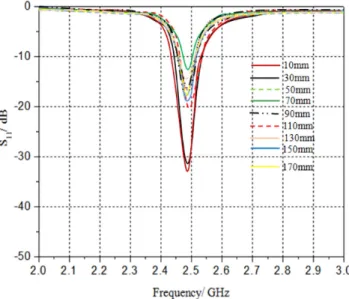
Next, to obtain the maximum gain enhancement, the proposed EBG layer is located to cover the microstrip antenna above the patch antenna this location of the EBG layer from the top of the patch is studied by running a parametric study. Therefore, the study starts with located the EBG layer above the patch from 10 mm to 190 mm with steps of 20 mm. It is found that the antenna perform the best gain at the boresight at 130 mm as can be seen in Fig. 8.
Fig. 6: Mesh view; (a) hexahedral mesh and (b) tetrahedral mesh.
Next, the focus on the effects of adding the EBG lens on antenna performance including the bandwidth, matching impedance, and frequency resonance is evaluated by monitoring the |S11| spectrum. Moreover, the gain, radiation efficiency, and the beamwidth are compared before and after introducing the proposed EBG structure. The |S11| spectra are presented in Fig.
7(a) from both cases: before and after adding the EBG lens. In the obtained |S11| spectrum, the change is found due to introducing the EBG lens that adds a capacitive coupling with the microstrip antenna [12]. It is concluded that the antenna shows a frequency resonance at 2.45 GHz, however, the resonance is shifted to 2.43 GHz after adding the EBG lens. The antenna gain is enhanced from 5.6 dBi up to 11.1 dBi after adding the EBG lens due to focusing the emerged beams from 99o to 26.7o as seen in Fig. 7(b), therefore by minimizing the beam in both ϑ- and φ- cut planes we will reach the maximum gain according to relation (1) [23].
30,000 G
O
(1) Insignificant decay is observed in the radiation efficiency of the microstrip antenna from 90% to 88.4% due to the effects of the conductor losses from the EBG structure. Such degradation is found to be much less than published degradation values; this because of the use of a single layer in the proposed design. From Fig. 7(b), the F/B ration is calculated using equation (2) [23].F/B= Gf – Gb (2) Where, Gf and Gb are the magnitude of the front lobe in dB value and the magnitude of the back lobe in
Fig. 7: Antenna performances with and without EBG lens; (a) |S11| spectrum and (b) Gain radiation pattern.
Next, to obtain the maximum gain enhancement, the proposed EBG layer is located to cover the microstrip antenna above the patch antenna this location of the EBG layer from the top of the patch is studied by running a parametric study. Therefore, the study starts with located the EBG layer above the patch from 10 mm to 190 mm with steps of 20 mm. It is found that the antenna perform the best gain at the boresight at 130 mm as can be seen in Fig. 8.
Next, the focus on the effects of adding the EBG lens on antenna performance including the bandwidth, matching im- pedance, and frequency resonance is evaluated by monitoring the |S11| spectrum. Moreover, the gain, radiation efficiency, and the beamwidth are compared before and after introducing the proposed EBG structure. The |S11| spectra are presented in Fig. 7(a) from both cases: before and after adding the EBG lens. In the obtained |S11| spectrum, the change is found due to introducing the EBG lens that adds a capacitive coupling with the microstrip antenna [12]. It is concluded that the an- tenna shows a frequency resonance at 2.45 GHz, however, the resonance is shifted to 2.43 GHz after adding the EBG lens. The antenna gain is enhanced from 5.6 dBi up to 11.1 dBi after adding the EBG lens due to focusing the emerged beams from 99o to 26.7o as seen in Fig. 7(b), therefore by minimizing the beam in both θ- and φ- cut planes we will reach the maximum gain according to relation (1) [23].
Fig. 6: Mesh view; (a) hexahedral mesh and (b) tetrahedral mesh.
Next, the focus on the effects of adding the EBG lens on antenna performance including the bandwidth, matching impedance, and frequency resonance is evaluated by monitoring the |S11| spectrum. Moreover, the gain, radiation efficiency, and the beamwidth are compared before and after introducing the proposed EBG structure. The |S11| spectra are presented in Fig.
7(a) from both cases: before and after adding the EBG lens. In the obtained |S11| spectrum, the change is found due to introducing the EBG lens that adds a capacitive coupling with the microstrip antenna [12]. It is concluded that the antenna shows a frequency resonance at 2.45 GHz, however, the resonance is shifted to 2.43 GHz after adding the EBG lens. The antenna gain is enhanced from 5.6 dBi up to 11.1 dBi after adding the EBG lens due to focusing the emerged beams from 99o to 26.7o as seen in Fig. 7(b), therefore by minimizing the beam in both ϑ- and φ- cut planes we will reach the maximum gain according to relation (1) [23].
30,000 G
O
(1) Insignificant decay is observed in the radiation efficiency of the microstrip antenna from 90% to 88.4% due to the effects of the conductor losses from the EBG structure. Such degradation is found to be much less than published degradation values; this because of the use of a single layer in the proposed design. From Fig. 7(b), the F/B ration is calculated using equation (2) [23].F/B= Gf – Gb (2) Where, G and G are the magnitude of the front
Fig. 7: Antenna performances with and without EBG lens; (a) |S11| spectrum and (b) Gain radiation pattern.
Next, to obtain the maximum gain enhancement, the proposed EBG layer is located to cover the microstrip antenna above the patch antenna this location of the EBG layer from the top of the patch is studied by running a parametric study. Therefore, the study starts with located the EBG layer above the patch from 10 mm to 190 mm with steps of 20 mm. It is found that the antenna perform the best gain at the boresight at 130 mm as can be seen in Fig. 8.
Fig. 6: Mesh view; (a) hexahedral mesh and (b) tetrahedral mesh.
Next, the focus on the effects of adding the EBG lens on antenna performance including the bandwidth, matching impedance, and frequency resonance is evaluated by monitoring the |S11| spectrum. Moreover, the gain, radiation efficiency, and the beamwidth are compared before and after introducing the proposed EBG structure. The |S11| spectra are presented in Fig.
7(a) from both cases: before and after adding the EBG lens. In the obtained |S11| spectrum, the change is found due to introducing the EBG lens that adds a capacitive coupling with the microstrip antenna [12]. It is concluded that the antenna shows a frequency resonance at 2.45 GHz, however, the resonance is shifted to 2.43 GHz after adding the EBG lens. The antenna gain is enhanced from 5.6 dBi up to 11.1 dBi after adding the EBG lens due to focusing the emerged beams from 99o to 26.7o as seen in Fig. 7(b), therefore by minimizing the beam in both ϑ- and φ- cut planes we will reach the maximum gain according to relation (1) [23].
30,000
G
O
(1) Insignificant decay is observed in the radiation efficiency of the microstrip antenna from 90% to 88.4% due to the effects of the conductor losses from the EBG structure. Such degradation is found to be much less than published degradation values; this because of the use of a single layer in the proposed design. From Fig. 7(b), the F/B ration is calculated using equation (2) [23].F/B= Gf – Gb (2) Where, Gf and Gb are the magnitude of the front lobe in dB value and the magnitude of the back lobe in
Fig. 7: Antenna performances with and without EBG lens; (a) |S11| spectrum and (b) Gain radiation pattern.
Next, to obtain the maximum gain enhancement, the proposed EBG layer is located to cover the microstrip antenna above the patch antenna this location of the EBG layer from the top of the patch is studied by running a parametric study. Therefore, the study starts with located the EBG layer above the patch from 10 mm to 190 mm with steps of 20 mm. It is found that the antenna perform the best gain at the boresight at 130 mm as can be seen in Fig. 8.
Insignificant decay is observed in the radiation efficiency of the microstrip antenna from 90% to 88.4% due to the ef- fects of the conductor losses from the EBG structure. Such degradation is found to be much less than published degrada- tion values; this because of the use of a single layer in the proposed design. From Fig. 7(b), the F/B ration is calculated using equation (2) [23].
Where, Gf and Gb are the magnitude of the front lobe in dB value and the magnitude of the back lobe in dB, respectively.
Next, to obtain the maximum gain enhancement, the pro- posed EBG layer is located to cover the microstrip antenna above the patch antenna this location of the EBG layer from the top of the patch is studied by running a parametric study.
Therefore, the study starts with located the EBG layer above the patch from 10 mm to 190 mm with steps of 20 mm. It is found that the antenna perform the best gain at the boresight at 130 mm as can be seen in Fig. 8.
Fig. 6: Mesh view; (a) hexahedral mesh and (b) tetrahedral mesh.
Next, the focus on the effects of adding the EBG lens on antenna performance including the bandwidth, matching impedance, and frequency resonance is evaluated by monitoring the |S11| spectrum. Moreover, the gain, radiation efficiency, and the beamwidth are compared before and after introducing the proposed EBG structure. The |S11| spectra are presented in Fig.
7(a) from both cases: before and after adding the EBG lens. In the obtained |S11| spectrum, the change is found due to introducing the EBG lens that adds a capacitive coupling with the microstrip antenna [12]. It is concluded that the antenna shows a frequency resonance at 2.45 GHz, however, the resonance is shifted to 2.43 GHz after adding the EBG lens. The antenna gain is enhanced from 5.6 dBi up to 11.1 dBi after adding the EBG lens due to focusing the emerged beams from 99o to 26.7o as seen in Fig. 7(b), therefore by minimizing the beam in both ϑ- and φ- cut planes we will reach the maximum gain according to relation (1) [23].
30,000 G
O
(1) Insignificant decay is observed in the radiation efficiency of the microstrip antenna from 90% to 88.4% due to the effects of the conductor losses from the EBG structure. Such degradation is found to be much less than published degradation values; this because of the use of a single layer in the proposed design. From Fig. 7(b), the F/B ration is calculated using equation (2) [23].F/B= Gf – Gb (2) Where, Gf and Gb are the magnitude of the front
Fig. 7: Antenna performances with and without EBG lens; (a) |S11| spectrum and (b) Gain radiation pattern.
Next, to obtain the maximum gain enhancement, the proposed EBG layer is located to cover the microstrip antenna above the patch antenna this location of the EBG layer from the top of the patch is studied by running a parametric study. Therefore, the study starts with located the EBG layer above the patch from 10 mm to 190 mm with steps of 20 mm. It is found that the antenna perform the best gain at the boresight at 130 mm as can be seen in Fig. 8.
Fig. 6: Mesh view; (a) hexahedral mesh and (b) tetrahedral mesh.
Fig. 7: Antenna performances with and without EBG lens; (a) |S11|
spectrum and (b) Gain radiation pattern.
A Systematic Analysis and Design of a High Gain Microstrip Antenna based on a Single EBG Layer
In this section, we investigate the effect of varying the distance between the EBG layer and the patch on resonant frequencies behavior. It is observed from Fig.
9, that insignificant change in the |S11| spectrum with respect to the distance between the EBG layer and the patch.
Fig. 9: Parametric-study based on the proposed EBG height in terms of |S11|.
A further investigation included the effect of varying the EBG planner array on resonant frequencies behavior. It is observed from Fig. 10, that insignificant change in the |S11| spectrum with respect to the EBG planner array except when the EBG array has one unit cell above the patch antenna.
Fig. 10: Parametric-study based on the proposed EBG planner array in terms of |S11|.
The boresight gain spectrum is evaluated using the two solvers in a frequency range from 2 GHz to 3 GHz as depicted in Fig. 11. From the obtained results in Fig.
11, the microstrip antenna without EBG layer exhibits an insignificant change in the antenna gain with respect to the gain spectrum that is presented by the antenna based EBG lens. Such difference is due to the high selectivity of the EBG structures for a particular frequency band as any frequency selective surface.
Nevertheless, varying the distance between the patch antenna and the EBG lens shows a significant change in the antenna gain. This is due to the fact of focusing the electromagnetic radiation at the numerical aperture of the lens relative to the electromagnetic aperture of the antenna as presented in [8]. Therefore, a numerical optimization process is invoked to validate the obtained results from the proposed algorithm in [8].
Fig. 11: Antenna boresight gain with and without EBG lens versus frequency.
The resonant frequency, |S11| spectra, gain, and bandwidth are given in Table II. It is found that the number of the EBG has a significant effect on the |S11| spectra, bandwidth and the gain.
TABLE IIANTENNA GAIN VERSUS THE NUMBER OF EBG PLANNER ARRAY
Gain (dBi) (MHz) B.W S11
Magnitude (dB) Resonant
Frequency (GHz) Number
of EBG planner array
6.4 31
-15.2 2.47
1 X 1
10.4 33
-16.8 2.467
3 X 3
11.1 43.2
-29.6 2.465
5 X 5
11.9 42.1
-24.1 2.462
7 X 7
12 42
-23.5 2.468
9 X 9
Next, the antenna 3D radiation patterns are evaluated with changing the EBG planner array as 1×1, 3×3, 5×5, 7×7, and 9×9 respectively. As seen in Fig.
12, the evaluated 3D radiation patterns are presented.
In this section, we investigate the effect of varying the distance between the EBG layer and the patch on resonant frequencies behavior. It is observed from Fig. 9, that insignifi- cant change in the |S11| spectrum with respect to the distance between the EBG layer and the patch.
A further investigation included the effect of varying the EBG planner array on resonant frequencies behavior. It is observed from Fig. 10, that insignificant change in the |S11| spectrum with respect to the EBG planner array except when the EBG array has one unit cell above the patch antenna.
The boresight gain spectrum is evaluated using the two solvers in a frequency range from 2 GHz to 3 GHz as
The resonant frequency, |S11| spectra, gain, and bandwidth are given in Table II. It is found that the number of the EBG has a significant effect on the |S11| spectra, bandwidth and the gain.
Next, the antenna 3D radiation patterns are evaluated with changing the EBG planner array as 1×1, 3×3, 5×5, 7×7, and 9×9 respectively. As seen in Fig. 12, the evaluated 3D radia- tion patterns are presented.
depicted in Fig. 11. From the obtained results in Fig. 11, the microstrip antenna without EBG layer exhibits an in- significant change in the antenna gain with respect to the gain spectrum that is presented by the antenna based EBG lens. Such difference is due to the high selectivity of the EBG structures for a particular frequency band as any fre- quency selective surface. Nevertheless, varying the distance between the patch antenna and the EBG lens shows a sig- nificant change in the antenna gain. This is due to the fact of focusing the electromagnetic radiation at the numerical aperture of the lens relative to the electromagnetic aperture of the antenna as presented in [8]. Therefore, a numerical optimization process is invoked to validate the obtained re- sults from the proposed algorithm in [8].
Fig. 9: Parametric-study based on the proposed EBG height in terms of |S11|.
Fig. 10: Parametric-study based on the proposed EBG planner array in terms of |S11|.
Fig. 11: Antenna boresight gain with and without EBG lens versus frequency.
DECEMBER 2018 • VOLUME X • NUMBER 4 27
Fig. 12: Comparison of the 3-radiation patterns with and without EBG at 2.45 GHz ; (a) patch only (b)1x1 (c) 3x3 (d) 5x5 (e) 7x7 (f)
9x9 EBG planer array respectively.
The antenna substrate area dimensions, length and width, are changed from 120×120mm2 to 240×240mm2 with a step of 40×40mm2. The other antenna dimensions are fixed. It is found that the proposed antenna |S11| spectra are affected significantly as seen in Fig. 13(a). However, the antenna gain is significantly affected as presented in Fig. 13(b).
Fig. 13: Parametric study simulation results; (a) |S11| spectra and (b) Antenna boresight gain.
The optimal antennae design performances are evaluated using HFSS software package for further validation [24] based Finite Element Method (FEM).
The antenna performances in terms of |S11| and radiation patterns are presented in Fig. 14. The obtained results reveal excellent agreements.
Fig. 14: Antenna performance comparison between three different techniques; (a) radiation patterns at. ϑ- 0o, (b) radiation patterns at
φ =0o, and (c) |S11| spectra.
The antenna substrate area dimensions, length and width, are changed from 120×120mm2 to 240×240mm2 with a step of 40×40mm2. The other antenna dimensions are fixed. It is found that the proposed antenna |S11| spectra are affected sig- nificantly as seen in Fig. 13(a). However, the antenna gain is significantly affected as presented in Fig. 13(b).
The optimal antennae design performances are evaluated using HFSS software package for further validation [24]
based Finite Element Method (FEM). The antenna perform- ances in terms of |S11| and radiation patterns are presented in Fig. 14. The obtained results reveal excellent agreements.
Fig. 12: Comparison of the 3-radiation patterns with and without EBG at 2.45 GHz ; (a) patch only (b)1x1 (c) 3x3 (d) 5x5 (e) 7x7 (f)
9x9 EBG planer array respectively.
The antenna substrate area dimensions, length and width, are changed from 120×120mm2 to 240×240mm2 with a step of 40×40mm2. The other
Fig. 13: Parametric study simulation results; (a) |S11| spectra and (b) Antenna boresight gain.
The optimal antennae design performances are evaluated using HFSS software package for further validation [24] based Finite Element Method (FEM).
The antenna performances in terms of |S11| and radiation patterns are presented in Fig. 14. The obtained results reveal excellent agreements.
Fig. 12: Comparison of the 3-radiation patterns with and without EBG at 2.45 GHz ; (a) patch only (b)1x1 (c) 3x3 (d) 5x5 (e) 7x7 (f) 9x9 EBG planer array respectively.
Fig. 13: Parametric study simulation results; (a) |S11| spectra and (b) Antenna boresight gain.
Fig. 14: Antenna performance comparison between three different techniques; (a) radiation patterns at. θ- 0o, (b) radiation patterns at
φ =0o, and (c) |S11| spectra.
A Systematic Analysis and Design of a High Gain Microstrip Antenna based on a Single EBG Layer
In the proposed simulation processes, the number of con- ducted mesh cells is Nx=280, Ny=225, and Nz=75 along the x-, y-, and z-axes, respectively. The required time step is 3.7×1024ns. However, the HFSS mesh to reach the conver- gence is found 4.5×10⁵ tetrahedral.
The achieved antenna enhancement is attributed to the fact of the summation of the emerging fields from the EBG unit cells according to the following equation:
In the proposed simulation processes, the number of conducted mesh cells is Nx=280, Ny=225, and Nz=75 along the x-, y-, and z-axes, respectively. The required time step is 3.7×1024ns. However, the HFSS mesh to reach the convergence is found 4.5×10⁵ tetrahedral.
The achieved antenna enhancement is attributed to the fact of the summation of the emerging fields from the EBG unit cells according to the following equation:
1
( , , )
So( , )
total S SL x y
S
g x y z h F v v
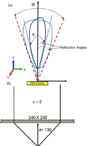
(3) where, gtotal is the total gain, hs is the antenna gain, and FSL is the unit cell geometrical function to be derived as in [8]. S is the central unit cell and So is the maximum number of the unit cells.The ray tracing is presented in Fig. 15 to describe the antenna beam radiation diffraction from the proposed EBG structure. It shows that the proposed EBG focuses the radiation in the paraxial beam direction.
Fig. 15: Ray tracing (a) Angles of the incident and refracted electromagnetic radiation rays and (b) Paraxial electromagnetic beam
ray modified by a zero refractive index lens.
IV. CONCLUSION
In this paper, a novel EBG geometry of a single layer positioned over a traditional microstrip antenna of a square patch is investigated for different wireless applications. In this design, the proposed antenna gain is improved from 5.6 dBi up to 11.1 dBi at 2.45 GHz with an F/B exceeds the 22 dB. It is found that the proposed EBG lens shows high improvement
selectivity around 2.45 GHz up to 2.55 GHz by providing a bore-sight gain over 11.1 dBi to fit the narrow bandwidth wireless communication systems.
Insignificant degradation in the radiation efficiency is taken place after introducing the proposed EBG lens due to the conductor losses. A numerical validation is obtained by using both TD and FD solves of CST MWS formulations to end up with an excellent agreement between the results the two solvers.
ACKNOWLEDGEMENT
The research reported in this paper was supported by the BME- Artificial Intelligence FIKP grant of EMMI (BME FIKP-MI/SC).
REFERENCES
[1] E. Yablonovitch, “Inhibited spontaneous emission in solid-state physics and electronics,” Phy. Rev. Lett., vol. 58, pp. 2059-2062, 1987.
[2] S. John, “Strong localization of photons in certain disordered dielectric superlattices,” Phy. Rev. Lett., vol. 58, pp. 2486-2489, 1987.
[3] T. A. Elwi, H. M. Al-Rizzo, Y. Al-Naiemy, and H.
R. Khaleel, “Miniaturized microstrip antenna array with ultra mutual coupling reduction for wearable MIMO systems,” 2011 IEEE International Symposium on Antennas and Propagation, July 2011.
[4] T. A. Elwi, M. M. Hamed, Z. Abbas, and M. A.
Elwi, “On the Performance of the 2D Planar Metamaterial Structure”, International Journal of Electronics and Communications, volume 68, Issue 9, pp. 846–850, September 2014.
[5] Z. Zhang and S. Satpathy, “Electromagnetic wave propagation in periodic structures: Bloch wave solution of Maxell’s equations,” Phy. Rev. Lett., vol. 65, pp.
2650-2653, 1990.
[6] K. M. Leung and Y. F. Liu, “Full vector wave calculation of photonic band structures in faced- centered-cubic dielectric media,” Phy. Rev. Lett., vol.
65, pp. 2646-2649, 1990.
[7] T. A. Elwi “A further investigation on the performance of the broadside coupled rectangular split ring resonators,” Progress In Electromagnetics Research Letters, volume 34, pp.1-8, August 2012.
[8] T. A. Elwi, H. M. Al-Rizzo, N. Bouaynaya, M. M.
Hammood, and Y. Al-Naiemy, “Theory of gain enhancement of UC–PBG antenna structures without invoking Maxwell’s equations: an array signal processing approach,” Progress In Electromagnetics Research B, volume 34, pp. 15-30, August 2011.
[9] T. A. Elwi, H. M. Al-Rizzo, D. G. Rucker, F.
Song, “Numerical simulation of a UC–PBG lens for gain enhancement of microstrip antennas,”
International Journal of RF and Microwave Computer- Aided Engineering, volume 19, issue 6, pp. 676–684, November 2009.
[10] T. A. Elwi, "A Slotted Lotus Shaped Microstrip Antenna based an EBG Structure", Journal of Material Sciences and Engineering, Vol. 7, issue 2, no. 439, pp.
1-15, March 2018.
where, gtotal is the total gain, hs is the antenna gain, and FSL is the unit cell geometrical function to be derived as in [8]. S is the central unit cell and So is the maximum number of the unit cells.
The ray tracing is presented in Fig. 15 to describe the antenna beam radiation diffraction from the proposed EBG structure. It shows that the proposed EBG focuses the radia- tion in the paraxial beam direction.
In the proposed simulation processes, the number of conducted mesh cells is Nx=280, Ny=225, and Nz=75 along the x-, y-, and z-axes, respectively. The required time step is 3.7×1024ns. However, the HFSS mesh to reach the convergence is found 4.5×10⁵ tetrahedral.
The achieved antenna enhancement is attributed to the fact of the summation of the emerging fields from the EBG unit cells according to the following equation:
1
( , , )
So( , )
total S SL x y
S
g x y z h F v v
(3) where, gtotal is the total gain, hs is the antenna gain, and FSL is the unit cell geometrical function to be derived as in [8]. S is the central unit cell and So is the maximum number of the unit cells.The ray tracing is presented in Fig. 15 to describe the antenna beam radiation diffraction from the proposed EBG structure. It shows that the proposed EBG focuses the radiation in the paraxial beam direction.
Fig. 15: Ray tracing (a) Angles of the incident and refracted electromagnetic radiation rays and (b) Paraxial electromagnetic beam
ray modified by a zero refractive index lens.
IV. CONCLUSION
In this paper, a novel EBG geometry of a single layer positioned over a traditional microstrip antenna of a square patch is investigated for different wireless applications. In this design, the proposed antenna gain is improved from 5.6 dBi up to 11.1 dBi at 2.45 GHz with an F/B exceeds the 22 dB. It is found that the
selectivity around 2.45 GHz up to 2.55 GHz by providing a bore-sight gain over 11.1 dBi to fit the narrow bandwidth wireless communication systems.
Insignificant degradation in the radiation efficiency is taken place after introducing the proposed EBG lens due to the conductor losses. A numerical validation is obtained by using both TD and FD solves of CST MWS formulations to end up with an excellent agreement between the results the two solvers.
ACKNOWLEDGEMENT
The research reported in this paper was supported by the BME- Artificial Intelligence FIKP grant of EMMI (BME FIKP-MI/SC).
REFERENCES
[1] E. Yablonovitch, “Inhibited spontaneous emission in solid-state physics and electronics,” Phy. Rev. Lett., vol. 58, pp. 2059-2062, 1987.
[2] S. John, “Strong localization of photons in certain disordered dielectric superlattices,” Phy. Rev. Lett., vol. 58, pp. 2486-2489, 1987.
[3] T. A. Elwi, H. M. Al-Rizzo, Y. Al-Naiemy, and H.
R. Khaleel, “Miniaturized microstrip antenna array with ultra mutual coupling reduction for wearable MIMO systems,” 2011 IEEE International Symposium on Antennas and Propagation, July 2011.
[4] T. A. Elwi, M. M. Hamed, Z. Abbas, and M. A.
Elwi, “On the Performance of the 2D Planar Metamaterial Structure”, International Journal of Electronics and Communications, volume 68, Issue 9, pp. 846–850, September 2014.
[5] Z. Zhang and S. Satpathy, “Electromagnetic wave propagation in periodic structures: Bloch wave solution of Maxell’s equations,” Phy. Rev. Lett., vol. 65, pp.
2650-2653, 1990.
[6] K. M. Leung and Y. F. Liu, “Full vector wave calculation of photonic band structures in faced- centered-cubic dielectric media,” Phy. Rev. Lett., vol.
65, pp. 2646-2649, 1990.
[7] T. A. Elwi “A further investigation on the performance of the broadside coupled rectangular split ring resonators,” Progress In Electromagnetics Research Letters, volume 34, pp.1-8, August 2012.
[8] T. A. Elwi, H. M. Al-Rizzo, N. Bouaynaya, M. M.
Hammood, and Y. Al-Naiemy, “Theory of gain enhancement of UC–PBG antenna structures without invoking Maxwell’s equations: an array signal processing approach,” Progress In Electromagnetics Research B, volume 34, pp. 15-30, August 2011.
[9] T. A. Elwi, H. M. Al-Rizzo, D. G. Rucker, F.
Song, “Numerical simulation of a UC–PBG lens for gain enhancement of microstrip antennas,”
International Journal of RF and Microwave Computer- Aided Engineering, volume 19, issue 6, pp. 676–684, November 2009.
[10] T. A. Elwi, "A Slotted Lotus Shaped Microstrip Antenna based an EBG Structure", Journal of Material Sciences and Engineering, Vol. 7, issue 2, no. 439, pp.
1-15, March 2018.
IV. CONCLUSON
In this paper, a novel EBG geometry of a single layer positioned over a traditional microstrip antenna of a square patch is investigated for different wireless applications. In
this design, the proposed antenna gain is improved from 5.6 dBi up to 11.1 dBi at 2.45 GHz with an F/B exceeds the 22 dB. It is found that the proposed EBG lens shows high im- provement selectivity around 2.45 GHz up to 2.55 GHz by providing a bore-sight gain over 11.1 dBi to fit the narrow bandwidth wireless communication systems. Insignificant degradation in the radiation efficiency is taken place after introducing the proposed EBG lens due to the conductor losses. A numerical validation is obtained by using both TD and FD solves of CST MWS formulations to end up with an excellent agreement between the results the two solvers.
ACKNOWLEDGEMENT
The research reported in this paper was supported by the BME- Artificial Intelligence FIKP grant of EMMI (BME FIKP-MI/SC).
REFERENCES
[1] E. Yablonovitch, “Inhibited spontaneous emission in solid- state physics and electronics,” Phy. Rev. Lett., vol. 58, pp.
2059-2062, 1987.
[2] S. John, “Strong localization of photons in certain disordered dielectric superlattices,” Phy. Rev. Lett., vol. 58, pp. 2486- 2489, 1987.
[3] T. A. Elwi, H. M. Al-Rizzo, Y. Al-Naiemy, and H. R. Khaleel,
“Miniaturized microstrip antenna array with ultra mutual coupling reduction for wearable MIMO systems,” 2011 IEEE International Symposium on Antennas and Propagation, July 2011.
[4] T. A. Elwi, M. M. Hamed, Z. Abbas, and M. A. Elwi, “On the Performance of the 2D Planar Metamaterial Structure”, International Journal of Electronics and Communications, volume 68, Issue 9, pp. 846–850, September 2014.
[5] Z. Zhang and S. Satpathy, “Electromagnetic wave propagation in periodic structures: Bloch wave solution of Maxell’s equations,” Phy. Rev. Lett., vol. 65, pp. 2650-2653, 1990.
[6] K. M. Leung and Y. F. Liu, “Full vector wave calculation of photonic band structures in faced-centered-cubic dielectric media,” Phy. Rev. Lett., vol. 65, pp. 2646-2649, 1990.
[7] T. A. Elwi “A further investigation on the performance of the broadside coupled rectangular split ring resonators,” Progress In Electromagnetics Research Letters, volume 34, pp.1-8, August 2012.
[8] T. A. Elwi, H. M. Al-Rizzo, N. Bouaynaya, M. M. Hammood, and Y. Al-Naiemy, “Theory of gain enhancement of UC–
PBG antenna structures without invoking Maxwell’s equations: an array signal processing approach,” Progress In Electromagnetics Research B, volume 34, pp. 15-30, August 2011.
[9] T. A. Elwi, H. M. Al-Rizzo, D. G. Rucker, F. Song, “Numerical simulation of a UC–PBG lens for gain enhancement of microstrip antennas,” International Journal of RF and Microwave Computer-Aided Engineering, volume 19, issue 6, pp. 676–684, November 2009.
[10] T. A. Elwi, “A Slotted Lotus Shaped Microstrip Antenna based an EBG Structure”, Journal of Material Sciences and Engineering, Vol. 7, issue 2, no. 439, pp. 1-15, March 2018.
[11] T. A. Elwi, A. I. Imran, and Y. Alnaiemy, “A Miniaturized Lotus Shaped Microstrip Antenna Loaded with EBG Structures for High Gain-Bandwidth Product Applications”, Progress In Electromagnetics Research C, volume 60, pp. 157-167, December 2015.
[12] A. I. Imran and T. A. Elwi, “A Cylindrical Wideband Slotted Patch Antenna Loaded with Frequency Selective Surface for MRI Applications” Engineering Science and Technology, an International Journal, volume 20, issue 3, pp. 990–996, April 2017.
[13] T. A. Elwi, “A Miniaturized Folded Antenna Array for MIMO Applications”, Wireless Personal Communications, in press, August 2017.
[14] T. A. Elwi, “Electromagnetic Band Gap Structures based an Ultra Wideband Microstrip Antenna”, Microwave and Optical Letters, volume 59, issue 4, pp. 827-834, February 2017.
[15] T. A. Elwi, “Toward Plasmonic UC-PBG Structures based SWCNTs for Optoelectronics Applications”, Diyala Journal for Pure Science, January 2018.
[16] T. A. Elwi and B. A. Ahmad, “A fractal metamaterial based printed dipoles on a nickel oxide polymer palm fiber substrate for Wi-Fi applications,” AEU-International Journal of Electronics and Communications, vol. 96, pp. 122-129, Sep. 2018.
[17] T. A. Elwi, “Metamaterial based a Printed Monopole Antenna for Sensing Applications,” International Journal of RF and Microwave Computer-Aided Engineering, volume 28, issue 7, pp. 1-10, Sep. 2018.
[18] T. A. Elwi, Z Abbas, M Noori, Y Al-Naiemy, EY Salih, MM Hamed, “Conformal antenna array for MIMO applications,”
Journal of Electromagnetic Analysis and Applications volume 6, issue 04, number 43, May 2014.
[19] T. A. Elwi, M. A. S. Al-Frieh, M. Bawi, “No Frequency Reuse:
Wearable Steerable MIMO Microstrip Antenna Array for Mobile Ad Hoc Applications,” British Journal of Applied Science &
Technology, volume 4, issue 17, pp. 2477-2488, June 2014.
[20] Y. Al-Naiemy, T. A. Elwi, and N. Lajos, “ Enhancing the Microstrip Antenna Gain Using a Novel EBG Lens Based on a Single Layer” 11th International Symposium on Communication Systems, Networks & Digital Signal Processing (CSNDSP), page (1-4) 27 September 2018.
[21] A. Bhutani, B. Göttel, D. Müller, and T. Zwick “Novel planar electromagnetic bandgap for mutual coupling reduction between patch antennas” 2015 German Microwave Conference page (1- 4), 14 May 2015.
[22] CST Microwave Studio, http://www.cst.com.
[23] C. A. Balanis, “Antenna Theory: Analysis and Design,” Wiley, John & Sons, Inc., NA, USA, Sep. 2008.
[24] HFSS, http://www.hfss.com.
Yahiea Alnaiemy was born in Iraq in 1971, in 1990; he was enrolled at the Higher Institution of Telecommunications and Post before transferring to Al-Mustansiriyah University/College of Engineering- Electrical Engineering Department in 1994. In July of 1998 he received a Bachelor‘s a Degree in Electrical Engineering. He continued his graduate studies by joining the Iraqi Commission for Computers and Informatics where he received a Higher Diploma in Information Systems in 2001. He enrolled at Diyala University as an instructor in communication Engineering, electrical power, computer and physics departments. In 2009 he was granted a scholarship to complete his master degree in electrical engineering at the University of Arkansas at Little Rock, USA. He got his MSc in Wireless Communications from UALR, USA, in 2012. While completing his graduate degree, his research effort has been in the area of antennas and microwave material characterization. In 2017 he was granted a scholarship to complete his Ph.D. in electrical engineering at Budapest University of Technology and Economics (BME), Hungary, His current research areas include UWB antennas, EBG structures, metamaterial, GPS, implantable wireless systems, and nanoscale microwave devices. He is one of the Member of IEEE and reviewer in PIER Journals since 2012.
Taha A. Elwi He received his B.Sc. in Electrical Engineering Department (2003), Postgraduate M.Sc. in Laser and Optoelectronics Engineering Department (2005) from Nahrain University Baghdad, Iraq. On January, 2008, he joined the University of Arkansas at Little Rock and he obtained his Ph.D. in December 2011 from the system engineering and science. His research areas include wearable and implantable antennas for biomedical wireless systems, smart antennas, Wi- Fi deployment, electromagnetic wave scattering by complex objects, design, modeling and testing of metamaterial structures for microwave applications, design and analysis of microstrip antennas for mobile radio systems, precipitation effects on terrestrial and satellite frequency re-use communication systems, effects of the complex media on electromagnetic propagation and GPS. The Nano-scale structures in the entire electromagnetic spectrum are a part of his research interest.
Lajos Nagy He received the Engineer option Communication) and PhD degrees, both from the Budapest University of Technology and economics (BME), Budapest, Hungary, in 1986 and 1995, respectively. He joined the department of Microwave Telecommunications (now Broadband Infocommunications and Electromagnetic Theory) in 1986, where he is currently an associate professor.
He has been the head of department of Broadband Infocommunications and Electromagnetic Theory in 2007. He is a lecturer on graduate and postgraduate courses at BME on Antennas and radiowave propagation, Radio system design, Adaptive antenna systems and Computer Programming. His research interests include antenna analysis and computer aided design, electromagnetic theory, radiowave propagation, communication electronics, signal processing and digital antenna array beamforming, topics where he has produced more than 100 different book chapters and peer-reviewed journal and conference papers. Member of Hungarian Telecommunication Association, official Hungarian Member and Hungarian Committee Secretary of URSI, Chair of the IEEE Chapter AP/
ComSoc/ED/MTT.