Kinetics of Sn whisker growth from Sn thin-films on Cu substrate
Balázs Illés1),2), Olivér Krammer1),2), Tamás Hurtony1), Karel Dusek2), David Busek2), Agata Skwarek3)
1) Department of Electronics Technology, Budapest University of Technology and Economics, Budapest, Hungary,
2) Department of Electrotechnology, Czech Technical University in Prague, Prague, Czech Republic
3) Łukasiewicz Research Network - Institute of Electron Technology, Kraków, Poland billes@ett.bme.hu
Abstract: The kinetics of Sn whisker growth was investigated on vacuum evaporated Sn thin- films. Sn film layers were deposited on a Cu substrate with 0.5 and 1 µm thicknesses. The samples were stored in room conditions (22±1°C / 50±5RH%) for sixty days. The Sn whiskers and the Cu-Sn layer structure underneath them were investigated with both scanning electron and ion microscopy. Fast Cu-Sn intermetallic formation resulted in considerable mechanical stress in the Sn layer, which initiated intensive whisker growth right after the layer deposition. The thinner Sn layer produced twice many whiskers compared to the thicker one. The lengths of the filament-type whiskers were similar, but the growth characteristics differed. The thinner Sn layer performed the highest whisker growth rates during the first seven days, while the thicker Sn layer increased the growth rate only after seven days. This phenomenon was explained by the cross-correlation of the stress relaxation ability of Sn layers and the amount of Sn atoms for whisker growth. The very high filament whisker growth rates might be caused by the interface flow mechanism, which could be initiated by the intermetallic layer growth itself. Furthermore, a correlation was found between the type of the whiskers and the morphology of the intermetallic layer underneath.
Keywords: tin whisker; thin-film; soldering; reliability; intermetallics.
1. Introduction
Sn whiskers are surface eruptions [1], which grow out spontaneously from high Sn content items applied in microelectronics like different surface coating layers [2] and solder joints [3].
According to the shape and size of the whisker, three main whisker types are distinguished:
hillock, nodule, and filament [4] The most dangerous, filament-type whiskers can reach even millimeters in length. Therefore, the whisker phenomenon exhibits a serious reliability risk in microelectronics due to the risk of short circuit formation. Sn whisker growth is always caused by strain-induced mechanical stress acting on the Sn-content item, and that can relax this stress via whisker growth. Usually, the following primary stress sources are distinguished: direct mechanical load (e.g., by connectors or test probes) [5], remaining residual stresses after Sn layer deposition [2], volumetric expansion/shrinkage in the Sn- content item (e.g., oxide and intermetallic growth) [6], and thermomechanical stresses [7].
The physical properties of the Sn grains, – size, shape, and crystallographic structure [8, 9]
– influence the propensity of whisker growth. A fine grain structure (grain size < 500 nm) enhances the grain boundary diffusion, so it results in fast intermetallic (IMC) layer growth [10, 11]. Furthermore, Sun et al. reported that under a long-term mechanical load, the increase in grain boundaries by the dislocations affects the whisker growth, since the new grain boundaries are the nucleation point of Sn whisker growth [12]. On the other hand, the higher number of grain boundaries (in a fine grain structure) increases the stress relaxation ability of the Sn-content item against mechanical stresses. The shape of the Sn grains has a similar effect: globular/horizontal grains have better stress relaxation ability than the columnar ones [13]. Furthermore, Yu et al. [14] reported that the wedge-type IMCs (which can cause significant mechanical stresses) form more frequently between the columnar grains then between horizontal ones. The crystallographic structure of the Sn grains can also influence on the whisker growth; it is more likely from Sn grains with a lower index than from higher ones [15, 16].
In the case of Sn layers on Cu substrates, the effect of Sn layer thickness on whisker growth is also significant. Thick Sn layers (>10 µm) perform slower and less intensive whisker growth than thin Sn layers (<1 µm) since the stress generated by the IMC formation needs more time to reach the top Sn grains and to create a mechanical strain on them [17]. Sn thin-films usually have a layer thickness of between 0.1–2 µm, and they are consists of micron-scale globular grains. These films are applied by the microelectronics industry as a bonding layer to Cu wires in the case of thermo-sonic wire-bonding technology [18], and as an anode material in lithium-ion batteries [19]. Firstly, Bozack et al. [20] and Chen and Shih [21] explained the Sn whisker growth in the case of 1–5 µm thick, vacuum evaporated, and sputtered Sn layers. Their explanation was based on the residual stress in the Sn layer, which might have been caused by a low background pressure (1 mTorr) applied during the layer deposition.
Later, the effect of the direct mechanical load was investigated. Chen and Chen [22]
deposited 1 μm thick Sn layer on a Cu layer and bent the samples. They found that the growth orientation of the Sn whiskers at the high tensile stress regions was random, but it was directional on the low tensile stress regions. Cheng et all. [23] observed fast Sn whisker growth in the case of 1 µm thick vacuum evaporated Sn layers on bent silicon substrates tested at 180 °C vacuum annealing. They explained the phenomenon with two different types of mass transport: the combination of interface fluid flow and grain boundary diffusion.
Howard et al. [24] also studied the role of interface flow mechanism in the extremely rapid tin whisker growth. Yang and Shi [25] derived a general equation, which describes mass transport during indentation-induced whisker growth from thin-films. Their equation based on the mass transport related to grain boundary diffusion and the grain boundary fluid flow.
Vianco et al. [26] studied the role of Dynamic Recrystallization (DRX) on whisker growth under different annealing temperatures and mechanical loads of 0.25–5 µm thick Sn layers evaporated on Si wafers. They found that continuous DRX took place in thicker (2–5 µm) Sn films and resulted in short whiskers. Killefer et al. [27] investigated the whisker growth on Sn thin-film subjected to a gamma-ray induced electric field. They found that electric charges generated in the insulating glass substrate under the Sn thin film were perpendicular to the Sn film, thus resulted in electrostatically driven whisker growth. Bora and Georgive [28]
investigated only the morphology of tin whiskers grown out from Sn thin-film on Cu substrate by FIB-facilitated TEM images. They found that the whiskers consisted of multiple filaments whose individual radii are in the range of tens of nanometers.
The aim of our investigation was to study the kinetics of Sn whisker growth from vacuum evaporated Sn thin-films on Cu substrate and to address the different effects of IMC formation on whisker growth. Furthermore, the relation between the stress relaxation ability of the Sn layer and the amount of Sn atoms for whisker growth was in the scope of our investigation.
2. Materials and Methods
Two different samples were fabricated with 0.5 and 1 μm thick Sn thin-film layers on Cu substrates. The preliminary preparation steps of the Cu substrates were the following: relaxing at 200 ºC for 3 hours; semi-automatic polishing to remove the surface scratches; chemical etching to remove the surface oxides, and cleaning in isopropyl alcohol to remove any contamination. The polishing was carried out in a crosshatched pattern with consecutive series of P600, P1200, and P4000 of SiC grinding papers. Then, a two-step fine-polishing process
was carried out on a buffer wheel, first with 3 μm and 1 μm diamond suspensions. The surface roughness of the Cu substrates was 0.187±0.015 μm without oriented scratches, (measured by an Alpha-Step 500 surface profiler). Sn layer deposition was performed by Electron Beam – Physical Vapour Deposition (EB-PVD) technology (Balzers BA 510 evaporator). Before the evaporation, the Cu substrates were neutralized by ion bombardment.
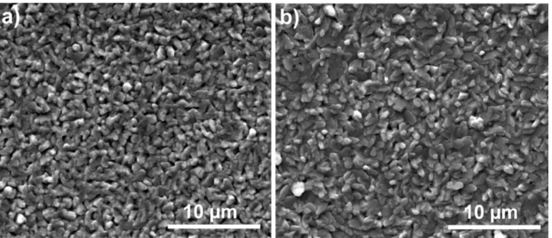
A 99.99% pure Sn was evaporated with 100 mA cathode heating current and 7 kV acceleration voltage in a high vacuum (10-3 Pa). Fig. 1a-b shows the SEM micrograph of the surface of the Sn thin-film layers. In this thickness range, the Sn grain size is determined by the layer thickness. It was found to be 0.25–0.5 μm and 0.5–1 μm in the case of the 0.5 µm and 1 μm thick Sn layers, respectively.
Fig. 1. The surface of the Sn thin-film layers: a) 0.5 µm thickness; b) 1 µm thickness.
Samples were stored at laboratory conditions (22±1°C/50±5RH%) up to sixty days.
Whisker growth was followed up by a Scanning Electron Microscope SEM (FEI Inspect S50).
The following statistical parameters of the Sn whiskers were calculated: the average area density, the average length of the filament-type whiskers, the maximum length of the filament-type whiskers, and the growth rate of the filament-type whiskers. From reliability aspects, mostly the length of filament-type whiskers is essential, since the short nodule-type whiskers cannot form short circuits. The statistical data were gained by a custom automatic image processing method. It based on an adaptive binarization algorithm to separate the whiskers from the surface of the samples. The binarization threshold is determined according to the mean intercept length of the developed structures (whiskers) on the investigated surface [29]. All points of the different statistics were calculated from 20 pcs. of SEM micrographs.
The axial length of the whiskers was measured according to the distance between the tip of the whisker, and the surface in accordance with the JESD201 standard. The view of the SEM
micrographs was perpendicular to the surface of the samples, which view provided the orthogonal projection of whiskers. According to the geometry theory, the whiskers must be longer than their orthogonal projections, so our results mean the minimal estimation of the whisker lengths. Surface-sections were prepared by a Dual-Beam Focused Ion Beam FIB (Thermo Scientific Scios 2). They were investigated by a FIB Scanning Ion Microscopy (FIB- SIM) to gain information about the microstructure of the Cu-Sn interface layer nearby the whiskers.
3. Results
3.1 Statistical results of Sn whisker growth
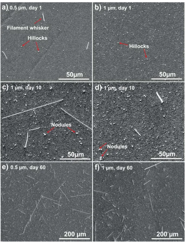
Sn whisker growth started right after the layer deposition. Fig. 2 shows a general overview of the samples at different stages. One day after layer deposition, both samples were full of hillocks (Fig. 2a-b), and the first filament whisker already appeared on 0.5 μm thick Sn layer (Fig. 2a). Nodule-type whiskers started to form 7–10 days after the layer deposition (Fig. 2c- d). During the sixty days period, many tin whiskers had been grown on both samples. The filament type whiskers reached even hundreds of micrometers, but most of the developed whiskers were nodule- and hillock-type (Fig. 2e-f).
Fig. 2. Whiskers on the samples: a) filament-type whiskers on 0.5 μm thick Sn layer after one day; b) numerous hillocks on 1 μm thick Sn layer after one day; c) all types of whiskers on 0.5 μm thick Sn layer after ten days; d) all types of whiskers on 1 μm thick Sn layer after ten days; e) numerous 50–300 µm long filament whiskers on 0.5 μm thick Sn layer after sixty days; f) numerous 50–200 µm long filament whiskers on 1 μm thick
Sn layer after sixty days.
Fig. 3 shows the average whisker densities, i.e., the specific number of whiskers on 1 mm2. Note that the logarithmic scale was used due to the 3 order of magnitude differences in the results between the initial and final stages of the investigation.
Fig. 3. The average density of Sn whiskers (all types).
The number of whiskers increased exponentially until the thirstiest days; later, some linear increase was observed in the case of 0.5μm thick Sn layer and a minor decrease in the case of 1μm thick Sn layers (it was probably caused by the break off of the whiskers). At the end of the inspection period, the average whisker density was 6 255 and 2 908 pcs./mm2 on 0.5 and 1μm thick Sn layers, respectively (Fig. 3). The ratios of the non-filament-type whiskers were very high but similar to each other, 95.4 and 92.9% on 0.5 and 1μm thick Sn layers, respectively.
The average length of the filament-type whiskers also almost saturated after thirty days (Fig. 4a), which means the considerable slow down of whisker growth.
Fig. 4. Length statistics of filament-type whiskers: a) average lengths; b) maximum lengths.
Generally, the differences were much smaller between the average lengths than between the average densities. After sixty days, the average length of filament whisker was 48.7 and 43.2 μm on 0.5 and 1μm thick Sn layers, respectively (Fig. 4a). The average length of the nodule- type whiskers was between 3–6 μm. The maximum length of the filament-type whiskers is the most important parameter of the whisker phenomenon since only a long whisker can cause short circuit failure. The maximum length of the filament-type whiskers did not saturate (Fig.
4b). The longest detected filament-type whisker was 621 and 463 μm on 0.5 and 1 μm thick Sn layers, respectively. These values are far beyond the pitch size of recently used fine-pitch components [30]. Therefore, it can be concluded that vacuum evaporated Sn thin films might be considered as a real risk in microelectronics.
3.2 Kinetics of the Sn whisker growth
Both statistical parameters of the filament-type whisker lengths (Fig. 4) showed a better stress relaxation ability of the 1 μm thick Sn layer during the first ten days of the study. On this sample, the growth of the filament-type whiskers was slower in the first period of the investigation (0–10 days), while in the second part of the experiments (10-60 days), they started to gain on the results of 0.5μm thick Sn layer.
Twenty-five filament-type whiskers were selected on both samples, and their rates of growth were measured to characterize precisely the kinetics of filament-type whisker growth.
Fig. 5 shows the individual growth rates and the averages of them.
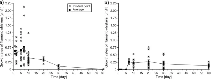
Fig. 5. Growth rates of the filament-type Sn whiskers: a) on 0.5 μm thick Sn layer; b) on 1 μm thick Sn layer.
As it could be predicted from the length statistics (Fig. 4), the 0.5 μm thick Sn layer performed the highest growth rates in the first seven days of the study (Fig. 5a). The maximum detected growth rate was 2.15 μm/h, and it was performed between the fifth and seventh days of the study. In this period, even the average growth rate was over 0.75 μm/h.
Ten days after the Sn layer deposition, the growth rates decreased, and in the second half of the study, only shallow values were detected. In the case of the 1 μm thick Sn layer, the growth rates increased only after seven days, and they remained near-constant (in average
~0.25 μm/h) until the end of the inspection. The highest detected growth rate was 0.8 μm/h between the tenth and twentieth days. These results supported the length characteristics (Fig.
4), namely how the results of the 1 μm thick Sn layer could gain on the results of the 0.5 μm thick Sn layer. The average time needed for a whisker to ultimately develop was around 200h in both cases.
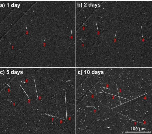
Fig. 6 presents the whisker growth of eight selected filament-type whiskers on the 0.5 µm thick Sn layer in the first ten days of the study. Note that the direction of a given whisker can change between the observations. Whiskers No. 1, 2, 3, and 4 already appeared one day after the layer deposition. They doubled their length up to two days after the layer deposition when whisker No. 5 appeared. Whiskers No. 1, 2, 3, and 4 doubled their length again up to five days after the layer deposition, till whisker No. 5 did not change, and whiskers No. 6, 7, and 8 appeared. Whiskers No. 2, 4, 6, and 8 growth further up to ten days after the layer deposition, till whiskers No. 1, 3, 5, and 7 did not change. The considerable differences in the whisker growth durations indicate that the driving force was not even on the surface of the sample.
Fig. 6. Growth kinetics filament-type Sn whiskers on 0.5 μm thick Sn layer: a) one day; b) two days; five days; ten days;
3.3 Microstructural analysis of the Sn-Cu layers
In order to examine the driving forces of the whisker growth, the microstructure of the Sn- Cu layers was investigated by FIB-SIM, sixty days after the layer deposition. Fig. 7 shows an example of each type of detected whisker. Noticeable IMC growth (marked by red lines) was detected in both samples. In the case of a 0.5 μm thick Sn layer, the IMC grains usually reached the surface of the Sn layer (Fig. 7c). In the case of a 1 μm thick Sn layer, it often did not happen (Fig. 7d), but exceptions were found (Fig. 7b). The IMC growth was similar in both cases, and it resulted in an average 300-500 nm thick IMC layer; however, differences were found in the shapes. Under filament-type whiskers (Fig. 7d), the IMC layer always formed a continuous layer. Under nodule-type whiskers (Fig. 7c), mostly large IMC islands consist of more grains) were detected. Under hillock-type whiskers (Fig. 7b), mostly narrow, scallop-type IMC grains were found.
Fig. 7. FIB examinations of the layer structure under the different type of Sn whiskers after sixty days: a) the investigated whiskers; b) hillock-type whisker on 1 μm thick Sn layer; c)
nodule-type whisker on 0.5 μm thick Sn layer; d) filament-type whisker on 1 μm thick Sn layer.
Discussion
The root cause of the significant Sn whisker growth was mainly the intensive IMC growth between the Cu substrate and the Sn thin-film layer. Most of the IMC growth during the Sn layer deposition, when the evaporated Sn reached the Cu surface and the Cu atoms diffused into the Sn thin-film layer. The test conditions were room conditions, and the test duration was only sixty days; therefore, negligible IMC growth occurred after the evaporation. The Cu- Sn system has two possible IMC phases; they are the Cu3Sn and the Cu6Sn5. The Cu3Sn develops directly at the Cu-Sn interface, and usually in a small amount compared to the Cu6Sn5, which grows on the Cu3Sn towards Sn film-layer [31]. The volume ratio of the developed Cu6Sn5 IMC is usually around 85-95% since the required energy for Cu3Sn formation is much higher than that for Cu6Sn5 formation.
The Cu6Sn5 has a higher density (8270 kg/m3) than the tin (7265 kg/m3); therefore, the formation of the IMC resulted in a volume shrinkage at the Cu-Sn interface. The volumetric
shrinkage generates mechanical stress inside the Sn film-layer [32, 33], which can be calculated by the following:
( )
KSn V V σ ∆
= υ ⋅
⋅ +
2 1 (1)
where KSn is Bulk modulus of Sn (58GPa), υ is the Poisson coefficient of Sn (0.36), and V is the given volume [m3]. Using Eq. 1, the specific mechanical stress for an equal volume is
~2.6GPa. Stress levels in the same order of magnitude were found in [33]. In addition, in the case of our Sn thin-film layers, the development of this stress was harsh and extensive, since the thickness ratios of the IMC layer and the Sn film-layer reached 50-80% (the average IMC layer thickness was between 300–500 nm).
The most significant difference between the obtained statistical results was the number of developed Sn whiskers. The 0.5μm thick Sn layer developed twice as many whiskers than the 1 μm thick Sn layer (Fig. 3). The large difference can be explained with the better relaxation ability of the 1 μm thick Sn layer against mechanical stresses since in a thicker layer, the critical IMC layer / Sn film-layer thickness ratio was usually not reached [17]. Generally, whisker growth slowed down considerably twenty days after the Sn deposition; later, mostly, the length of already existing whiskers increased. This phenomenon was caused by the cross- correlation of the stress relaxation ability and the consumption of the Sn film-layer, which properties determined by the thickness of the Sn layer. This hypothesis was supported by the final length statistics of the filament-type whisker (averages and maximums), which were similar in both cases (Fig. 4), but with very different growth characteristics in time.
The growth characteristics showed, that on 0.5 μm thick Sn layer, whisker growth was the most intensive until the seventh day of the study, later the growth rates decreased significantly, and the whisker growth almost stopped after thirty days (Fig. 5a). Parallelly, the 1 μm thick Sn layer could relax the mechanical stress until the fifth day but later showed near- constant whisker growth rate until the end of the study (Fig. 5b). These growth characteristics showed the relation between the relaxation ability of the layers and the amount of Sn in the layers. The thinner Sn layer (0.5 μm) could not stand the great mechanical stress and started considerable whisker growth right after the layer deposition, however available Sn atoms for whisker growth had been consumed rapidly. Although a thicker Sn layer (1 μm) could relax the mechanical stress for a while, on the other hand, the higher amount of Sn atoms could maintain the whisker growth longer than in the case of the thinner Sn layer.
The maximum detected whisker growth rate reached 2.15 μm/h between the fifth and seventh day on 0.5 μm thick Sn layer. This extremely fast whisker growth cannot be
explained by classical whisker growth models like Sn mass transfer via grain boundary diffusion [24], grain boundary migration, or sliding [7]. Classical models can approve maximum whisker growth rates like 0.03-0.05 µm/h [34, 35], which are two orders of magnitude smaller than the maximum calculated values in the present study. To be able to explain such high whisker growth rates, Tu and Li derived “the grain boundary fluid flow theory” [34]. It was developed further by Cheng et al. [36] and Howard et al. [24], and it is referred as interface flow theory, which can explain the extremely fast mass transport of Sn atoms in a plastic state along with the interface of the IMC layer and the Sn film-layer. It must be noted that Change et al. and Howard et al. observed the interface flow only in the case of the real external mechanical load of the samples.
Our hypothesis is that the extremely high mechanical stress caused by the IMC layer growth could initiate the interface flow mechanism in the Cu-Sn system. The mechanical stress could plasticize the Sn at the interface of the IMC layer, and the Sn thin-film layer and these Sn atoms could form a fluid-like viscous layer. This viscous layer could have constantly been flowing towards the lower stress regions of the Sn thin-film layer, which were the root grains of the whiskers [4], and it could have been supporting the necessary amount of Sn atoms for forming the whisker. The interface flow mechanism could cause very high whisker growth rates until the mechanical stress existed and/or the Sn atoms were available. It has to be noted that direct evidence was not found on the interface flow mechanism. Our hypothesis is based on the calculated high mechanical stress and the observed extreme whisker growth rates.
The relation between the morphology of the IMC layer and the whisker growth was investigated in many studies before. However, these studies usually tried to find only the correlation between the roughness of the IMC layer and the propensity of whisker growth [37, 38]. Basically, it is accepted that an uneven IMC layer can generate higher mechanical stress and more Sn whiskers than a uniform one [38, 39] due to the larger active surface of the IMC layer. Compared to 2 μm thick Sn film-layers – where almost only filament-type whiskers were found [40] –, the amount of the non-filament-type whiskers (mainly the hillocks) were very high in the present study (over 90% from the total amount of whiskers). The reasons for this considerable difference could be seen in the FIB-SIM micrographs. Namely, a correlation was found between the morphology of the IMC layer and the type Sn whiskers.
Under the hillock-type whiskers, the IMC layer was usually uneven (Fig. 7b), it was not even layer-like — only scallop-type IMC grains were found. Under the nodule-type whiskers, the IMC layer was usually more layer-like, with large IMC islands. Under the filament-type
whiskers, always continuous IMC layer was observed. The Sn thin-film layers could not stand even smaller stress by the uneven IMC layer and started whisker formation readily. However, the formation stopped very soon, and a high amount of short, hillock-type whiskers were formed. The other factor of the more frequent appearance of nodule-type whiskers in the present study was the easier diffusion of Cu atoms from the substrate into the whisker bodies.
The Cu contaminants might twist the whisker body and result in the formation of nodule-type whiskers [41]. In the case of 2 μm thick Sn layer [40], the Cu atoms needed more time to reach the root of the whiskers, and it delayed the distortion of the regular geometry of the formed whiskers.
5. Conclusions
The kinetics of Sn whisker growth was investigated in the case of Sn thin-films on Cu substrates. The Cu6Sn5 IMC formation resulted in considerable mechanical stress in the Sn layer, which initiated intensive whisker growth right after the layer deposition. The observed kinetics of the whisker growth was probably determined by the cross-correlation of the stress relaxation ability of the Sn layer and the amount of Sn atoms for whisker growth. The thinner Sn layer started whisker growth right after the layer deposition, but available Sn atoms consumed fastly by the IMC formation. The thicker Sn layer relaxed the mechanical stress longer, but it could maintain the whisker growth longer. Generally, the decrease of the Sn film-layer thickness increased the number of whiskers but did not increase the maximal length of whisker considerably. The length of the filament-type whiskers reached hundreds of micrometers, and it can cause serious reliability risk in microelectronic. The high filament whisker growth rates might be caused by the interface flow mechanism, which could be initiated by the IMC layer growth itself. Furthermore, a correlation was found between the types of the whiskers and the morphology of the IMC layer underneath them. Under the hillock-type whiskers, the IMC layer was usually uneven with scallop-type IMC grains.
Under the nodule-type and filament-type whiskers, the IMC layer was usually more continuous layer-like. As the main conclusion of this work, it is suggested to increase the thickness of the Sn thin-films in microelectronic applications.
Acknowledgment: The reported research was partially financed by the National Research, Development, and Innovation Office of Hungary (FK 127970), by the Higher Education Excellence Program of the Ministry of Human Capacities in the frame of “Nanotechnology
and Materials Science research area of Budapest University of Technology and Economics”
(BME FIKP-NAT).
Data availability statement
The raw/processed data required to reproduce these findings cannot be shared at this time as the data also forms part of an ongoing study.
References:
[1] F. Otsubo, H. Era, Y. Tsuru, S. Hirano, TEM analysis of whiskers formation over tin- plated films Materials Chemistry and Physics 251, 122985 (2020)
[2] H.P. Lim, A. Ourdjini, T.A.A. Bakar, T. Tesfamichael, The effects of humidity on tin whisker growth by immersion tin plating and tin solder dipping surface finishes, Procedia Manuf. 2, 275 – 279 (2015)
[3] B. Illés, T. Hurtony, B. Medgyes, Effect of current load on corrosion induced tin whisker growth from SnAgCu solder alloys, Corros. Sci. 99, 313-319 (2015)
[4] B. Illés, A. Skwarek, R. Bátorfi, J. Ratajczak, A. Czerwinski, O. Krammer, B. Medgyes, B. Horváth, T. Hurtony, Whisker growth from vacuum evaporated submicron Sn thin films, Surf. Coat. Tech 311, 216-222 (2017)
[5] I. Lujan-Regalado, A. Kirubanandham, J.J. Williams, N. Chawla, Nucleation and Growth of Tin Hillocks by In Situ Nanoindentation, J. Electron. Mater. 48, 58–71 (2019)
[6] Y. Liu, P. Zhang, Y.M. Zhang, J. Ding, J.J. Shi, Z.M. Sun, Spontaneous growth of Sn whiskers and a new formation mechanism, Mater. Lett. 178, 111–114 (2016)
[7] F.C. Walsh, C.T.J. Low, A review of developments in the electrodeposition of tin, Surf.
Coat. Tech. 288, 79–94 (2016)
[8] M.A. Ashworth, G.D. Wilcox, R.L. Higginson, R.J. Heath, C. Liu, R.J. Mo, The effect of electroplating parameters and substrate material on tin whisker formation, Microelectron.
Reliab. 55, 180–191 (2015).
[9] P. Sarobol, J.E. Blendell, C.A. Handwerker, Whisker and hillock growth via coupled localized Coble creep, grain boundary sliding, and shear induced grain boundary migration, Acta Mater. 61, 1991–2003 (2013)
[10] Y. Tian, J. Han, L. Ma, F. Guo, The dominant effect of c-axis orientation in tin on the electromigration behaviors in tricrystal Sn-3.0Ag-0.5Cu solder joints, Microelectron.
Reliab. 80, 7–13 (2018).
[11] L. Ma, Y. Zuo, S. Liu, F. Guo, A. Lee, K.N. Subramanian, Whisker growth behaviors in POSS-silanol modified Sn3.0Ag0.5Cu composite solders, J. Alloy. Compd. 657, 400–407 (2016)
[12] M. Sun, M. Dong, D. Wang, H. Ling, A. Hu, M. Li, Growth behavior of tin whisker on SnAg microbump under compressive stress, Scripta Mater. 147, 114–118 (2018) [13] L. Sauter, A. Seekamp, Y. Shibata, Y. Kanameda, H. Yamashita, Whisker mitigation
measures for Sn-plated Cu for different stress tests, Microelectron. Reliab. 50, 1631-1635 (2010)
[14] C.-F. Yu, C.-M. Chan, K.-C. Hsieh, The effect of tin grain structure on whisker growth, Microelectron. Reliab. 50, 1146–1151 (2010)
[15] P. Jagtap, A. Chakraborty, P. Eisenlohr, P. Kumar, Identification of whisker grain in Sn coatings by analysing crystallographic micro-texture using electron back-scatter
diffraction, Acta Mater. 134, 346-359 (2017)
[16] P. Eckold, M.S. Sellers, R. Niewa, W. Hügel, The surface energies of β-Sn — A new concept for corrosion and whisker mitigation, Microelectron Reliab. 55, 2799–2807 (2015)
[17] B. Horváth, B. Illés, T. Shinohara, G. Harsányi, Whisker Growth on Annealed and Recrystallized Tin Platings, Thin Solid Films 520, 5733-5740 (2012)
[18] I. I. Beilis, Y. Koulik, R. L. Boxman, D. Arb, Thin film deposition using a plasma source with a hot refractory anode vacuum arc, J. Mater. Sci. 45, 6325–6331 (2010)
[19] R. Hu, H. Liu, M. Zeng, J. Liu, M. Zhu, Progress on Sn-based thin-film anode materials for lithium-ion batteries, Chin. Sci. Bull. 57, 4119-4130 (2012)
[20] M.J. Bozack, E.R. Crandall, C.L. Rodekohr, R.N. Dean, G.T. Flowers, J.C. Suhling, High Lateral Resolution Auger Electron Spectroscopic (AES) Measurements for Sn Whiskers on Brass, IEEE Trans. Elect. Packag. Manuf., 33, 198-204 (2010).
[21] C. Chen, P. Shih, A peculiar composite structure of carbon nanofibers growing on a microsized tin whisker, J. Mater. Res. 23, 2668 – 2673 (2008)
[22] C. Chen, Y. Chen, Growth orientation of the tin whiskers on an electrodeposited Sn thin film under three-point bending, Mater. Let. 63, 1517–1520 (2009).
[23] J. Cheng, P.T. Vianco, B. Zhang, J.C.M. Li, Nucleation and growth of tin whiskers, Appl. Phys. Lett. 98, 241910 (2011).
[24] H.P. Howard, J. Cheng, P.T. Vianco, J.C.M. Li, Interface flow mechanism for tin whisker growth, Acta Mater. 59, 1957–1963 (2011).
[25] F. Yang, Y. Shi, Analysis of whisker growth on a surface of revolution, Phy. Let. A 381, 2767–2771 (2017).
[26] P.T. Vianco M.K. Neilsen, J.A. Rejent, R.P. Grant, Vallidation of the Dynamic
Recrystallization (DRX) Mechanism for Whisker and Hillock Growth on Sn Thin Films, J. Electron. Mater 44, 4012-4033 (2015).
[27] M. Killefer, V. Borra, A. Al-Bayati, D.G. Georgiev, V.G. Karpov, E.I. Parsai. D.
Shvydka, Whisker growth on Sn thin film accelerated under gamma-ray induced electric field, J. Phy. D: App. Phy. 50, 405302 (2017)
[28] V. Borra, D.G. Georgiev, Microscopic Structure of Metal Whiskers, Phy. Rev. App. 9, 054029 (2018)
[29] O. Krammer, B. Illés, R. Bátorfi, K. Dušek, Automatic characterisation method for statistical evaluation of tin whisker growth, Microelectron Reliab. 73, 14-21 (2017) [30] A. Géczy, Z. Illyefalvi-Vitez, Package–on–package–review on a promising packaging
technology, In proceedings of 33rd International Spring Seminar on Electronics Technology, ISSE, Warsava, Poland, pp. 117-122 (2010).
[31] B. Illés, A. Skwarek, J. Ratajczak, K. Dušek, D. Bušek, The influence of the crystallographic structure of the intermetallic grains on tin whisker growth, J. Alloy.
Compnd. 785, 774-780 (2019).
[32] J.F. Li, P.A. Agyakwa, C.M. Johnson, A numerical method to determine interdiffusion coefficients of Cu6Sn5 and Cu3Sn intermetallic compounds, Intermetallics 40, 50-59 (2013)
[33] W.J. Boettinger, C.E. Johnson, L.A. Bendersky, K.-W. Moon, M.E. Williams, G.R.
Stafford, Whisker and Hillock formation on Sn, Sn–Cu and Sn–Pb electrodeposits, Acta Mater. 53, 5033–5050 (2005)
[34] K.N. Tu, J.C.M. Li, Spontaneous whisker growth on lead-free solder finishes, Mater. Sci.
Eng. A 409, 131–139 (2005)
[35] E.N. Hoffman, M.W. Barsoum, W. Wang, R.D. Doherty, A. Zavaliangos, On the spontaneous growth of soft metallic whiskers, in Proceedings of IEEE 51th Holm Conference on Electrical Contacts, USA, pp. 121-126 (2005)
[36] J. Cheng, P.T. Vianco, J.C.M. Li, Hollow tin/chromium whiskers, Appl. Phys. Lett. 96, 184102 (2010).
[37] K.S. Kim, C.H. Yu, S.W. Han., K.C. Yang, J.H. Kim, Investigation of relation between intermetallic and tin whisker growths under ambient condition, Microelectron. Reliab. 48, 111-118 (2008).
[38] W. Zhang, A. Egli, F. Schwager, and N. Brown, Investigation of Sn–Cu intermetallic compounds by AFM: New aspects of the role of intermetallic compounds in whisker formation, IEEE Trans. Elect. Packag. Manuf. 28, 85–93 (2005).
[39] K.S. Kim, J.M. Yang, J.P. Ahn, The effect of electric current and surface oxidization on the growth of Sn whiskers, Appl. Surf. Sci. 256, 7166-7174 (2010).
[40] B. Illés, T. Hurtony, O. Krammer, B. Medgyes, K. Dusek, D. Busek, Effect of Cu substrate roughness and Sn layer thickness on whisker development from Sn thin-films, Materials 12, 3609 (2012).
[41] B. Horváth, Influence of copper diffusion on the shape of whiskers grown on bright tin layers, Microelectron. Reilab. 53, 1009-1020 (2013).