Early Stage Whisker Development from Sn Thin Film on Cu Substrate
Balázs Illés1), Tamás Hurtony1), Olivér Krammer1), Réka Bátorfi1), Bálint Medgyes1), Gábor Harsányi1) 1) Department of Electronics Technology, Budapest University of Technology and Economics,
Budapest, Hungary billes@ett.bme.hu
Abstract: The Sn thin film on Cu substrate has high Sn whisker growth susceptibility because of the intensive Cu6Sn5 intermetallic formation at the Sn-Cu interface. In this study, the whisker development on vacuum evaporated Sn thin film deposited on Cu substrates was investigated, starting directly from the Sn deposition. The aim was to obtain more information about the whiskering behavior of Sn thin film in the early stage of the life cycle. For the study, 99.99% pure tin was vacuum evaporated onto Cu substrates. Two different Cu substrates were applied with different surface roughness to investigate the effect of surface roughness on the whisker development. The average thickness of the evaporated Sn layer was ~2 μm. Samples were stored at room temperature for 10 weeks. Whisker development was observed by scanning electron microscope. It was found that the large compressive stress in the Sn layer because of the intermetallic formation initiates the whisker development even after 1 day of the Sn layer deposition. Almost only filament type whiskers were detected. The characteristics of the whisker density showed exponential saturation up to 10 days of the study, while the length of the whiskers was growing further still the end of the study. It was also found that the surface roughness of the Cu substrate affects the rate of whisker growth.
1.INTRODUCTION
Sn whiskers are surface eruptions which can have mono- or polycrystalline structure, and their usual dimensions are 1–10 µm in thickness and 10–500 µm in length [1]. The dimensions depend on the type of whisker, which can be hillock, nodule or filament type. They can develop from any types of high Sn content structure, like surface coatings, solder joints or thin film layers [2]. Sn whiskers can cause serious reliability problems in microelectronics, since they can form short circuits in fine pitch electronics. Transition to lead-free electronics in 2006 resulted in the application of pure Sn as surface finishes on Cu wirings, and high Sn content solder alloys (>98%wt) [3-5]. Unfortunately, the Cu-Sn
layer structure is very sensitive to whisker development due to the Cu6Sn5 Intermetallic Layer (IML) growth at the interface, which yields in compressive stress in the Sn layer [6]. The whisker development acts like a stress release mechanism for the Sn layer against compressive stresses.
However, the physical properties of the Sn layer, both the grain size [7] and the layer thickness [8]) affect the whisker susceptibility of the layer. In the case of fine grain structure of the layer (grain size < 500 nm), the diffusivity is faster due to larger amount of grain boundaries, so the electro- migration causes rapid IML growth [9]. From the other hand, fine grain structure (with many grain boundaries) aids the stress relaxation of the Sn layer against compressive stress. In the case of thick Sn layer on Cu substrate (> 10 µm), the Sn whisker development is slower and less intensive than that on thin Sn layers (< 5 µm), since more nucleation time is necessary for the intermetallic compounds in thick layers to reach the grain boundaries of the Sn grains at the surface and to form compressive stress [10].
The vacuum evaporation results in layer thickness between 0.1–4 µm. Although the microelectronics industry mostly applies thicker Sn layers, the Sn and Cu-Sn thin films are also used as bonding layer to Cu wires [11], and as anode material in lithium-ion batteries [12]. In the case of Sn thin film, the effect of direct mechanical load was investigated mostly. Chen and Chen did investigation on bended Cu substrates with 1 μm thick Sn thin film. They found numerous whiskers at the high tensile stress regions [13]. Cheng et al. investigated the behavior of 1 µm thick Sn thin film on bent silicon substrates at 180 °C vacuum annealing. They found that in the whisker growth two types of mass transport take place: the interface fluid transport and vertical grain boundary diffusion [14].
In our previous study [4], considerable Sn whisker development was found from 1 μm thick Sn thin film on Cu substrate stored at room temperature. After 2 weeks from the layer deposition, the longest filament whiskers reached 175 µm and the average whisker density was 2800 pcs./mm2. Indirect evidences were found that the high stress due to the IML formation could initiate an interface flow mechanism [15] between the Sn layer and the IMC layer which caused this very intensive whisker growth [4]. In this study, our aim was to investigate the early stage whisker development from Sn thin film on different Cu substrates, starting directly from the Sn deposition.
2.MATERIALS AND METHODS
For the study, 99.99% pure tin was vacuum evaporated onto Cu substrates by Electron Beam – Physical Vapour Deposition (EB-PVD) method (Balzers BA510 evaporator). Two types of Cu
substrates were applied with rougher and finer surfaces (prepared by mechanical polishing) to investigate the effect of surface roughness on the whisker development. Before the evaporation, the Cu substrates were relaxed at 200 ºC for 3 hours. Later the surface oxides were separated by chemical etching
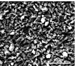
Fig. 1. SEM micrograph of the Sn thin film on finer Cu substrate with fine surface roughness right after the deposition.
The samples were cleaned in isopropyl alcohol and were neutralized by ion bombardment (directly in the evaporator). The applied cathode heating current was 100 mA with 7 kV acceleration voltage. A high vacuum (10-3 Pa). The evaporation lasted for 10 minutes, which resulted in an average layer thickness of 2 µm with ~1–2 µm grain size (Fig. 1). The layer thickness was measured on cross- sections prepared by Thermo Scientific Scios 2 Dual-Beam Focused Ion Beam (FIB). The samples were stored at room temperature for 70 days.
Whisker development was checked by a FEI Inspect S50 Scanning Electron Microscope (SEM), (Acc. Voltage 20 kV). Since our aim was to study the early stage of the whisker development, the measurements were more frequent till the first 20 days (in each 2–5 days); later on, the samples were investigated only at 35 and 70 days. Whisker densities and lengths were measured on SEM micrographs by an automatic image processing method. The method based on an adaptive binarisation algorithm which separates the whiskers from the surface of the samples. The binarisation is based on calculating the Mean Intercept Length (MIL) of the whiskers [16]. The applied unit of the whisker density calculations was pcs./mm2. The length of a whisker was calculated by the length of major axis
of overlaying ellipses on the whiskers. The statistical parameters were calculated from 20 measurement results.
3.RESULTS AND DISCUSSIONS
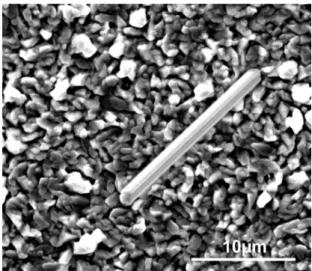
The large compressive stress by the IML formation initiates the whisker development right 1 day after the deposition. Almost only filament type whiskers were detected (Fig. 2). This was unexpected according to our previous results where most of the whiskers were nodule type (like in [4]). The root cause could be the larger thickness of the Sn layer here, which could block the diffusion of Cu atoms into the whiskers. The contaminating atoms in the whisker body can cause the twisting of the whisker and forms the nodule type whisker [17]. However, further research is necessary in this topic.
The SEM micrographs in Fig. 3–5 illustrate the development of the whiskers on the same area at 3 time-steps with 500x magnification. The main conclusions of the SEM observations are the following:
the number of the whiskers increased mainly at the first part of the test. Later, only the length increased of the already developed whiskers. In addition, much less whisker was developed than in our previous study with 400 nm thick Sn film [4].
Fig. 2. Filament type Sn whisker (17 μm long) 1 day after of the deposition (on polished Cu substrate).
Fig. 3. Sn whiskers 5 days after the deposition (on rougher Cu substrate).
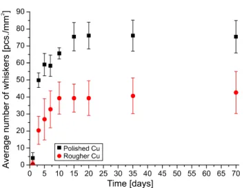
The results of the statistical evaluation support the conclusions of the SEM evaluation. The three main parameters of the whisker growth were calculated: the whisker density, the average length of the whiskers and the maximum length of the whiskers. The whisker density increased only until 10–
15 days, and reached 40 and 75pcs./mm2 on the rougher and polished Cu substrates, respectively (Fig.
6). In the case of 400 nm thick Sn thin film, the whisker density increased till 90 days after the deposition and its value was one and a half magnitude higher, 3900 pcs./mm2. This difference in height can be explained with the better relaxation ability of the 5 times thicker Sn film against the mechanical stress and by the the lack of nodule whiskers in this study. (Note that in the previous study most of the developed whisker were nodule type [4]).
Fig. 4. Sn whiskers 20 days after the deposition (on rougher Cu substrate).
Fig. 5. Sn whiskers 70 days after the deposition (on rougher Cu substrate).
The average length of the Sn whiskers exhibited also saturation type characteristics by 35 days on both samples (Fig. 7). However, some increase was still found at 70 days. Interestingly, the previously mentioned trend was changed after 15 days of the layer deposition; namely longer whiskers were found on the samples with rougher substrate surface (in average 42 μm at 70 days) than on the samples with polished substrate surface (in average 25 μm at 70 days). In the case of 400nm thick Sn thin film, the average whisker length was much lower, only around 7μm due to the high number of short nodule whiskers [4].
Fig. 6. Density of Sn whiskers.
Fig. 7. Average length of Sn whiskers.
The maximum length of the developed Sn whisker is the most important parameter, since only one but long whisker can cause reliability problems in microelectronics. Unfortunately, these characteristics did not show any saturation, the rate of growth was linear till the end of the study (Fig. 8). The longest detected Sn whisker was 420 µm and 200 μm on the samples with rough and polished Cu substrates, respectively. These values are far beyond the pitch size of recently used fine-pitch components [18, 19]. Therefore, it can be concluded that vacuum evaporated Sn thin films are real risk in microelectronics. The maximum whisker lengths were very similar to the results of the 400 nm thick Sn layer, where the longest whisker was 275 μm 70 days after the layer deposition. Despite of the larger mechanical stress in the thinner Sn layers, the less amount of Sn probably blocks the development of longer whiskers.
Fig. 8. Maximum length of Sn whiskers.
The differences between the samples with rough and polished Cu substrate are interesting.
Generally, the samples with rougher Cu surface produced less but longer whisker than the samples with polished Cu surface (all results are separated statistically). Investigating the statistical results more deeply, they showed that the whisker development is more intensive on the samples with polished Cu surface, till 10 days after the Sn deposition. Not just more but longer whiskers grew on these samples.
After 10 days, the samples with rough Cu surface showed already longer whiskers till the end of the study.
Our theory is that on the rougher Cu substrate the formation of wedge type intermetallics is more possible which can produce larger mechanical stress leads to longer whiskers [4, 8], however the stress development is somehow faster on the polished Cu substrate. This must be proven with further and deeper investigations of the Sn-Cu layer structure.
Generally, the stress development was very uniform on the whole surface of the samples, since the deviation in layer thickness were low compared to other Sn whisker studies. The mechanical stress by the IML growth decreased considerably up to 10 days after the Sn deposition, since most of the whiskers were developed up to then. Later, the IML growth could not produce more whiskers but could only increase the length of the existing ones.
4.CONCLUSIONS
In this study, the early stage whisker development from 2 μm thick vacuum evaporated Sn film on rough and polished Cu substrates were investigated. It was found, that the whisker development started already after 1 day and most of the whisker formed up to 10 days after the Sn deposition. Later, only their length increased till the end of the study. The number of the developed whiskers was not extremely high, but their length was significant, since almost only filament type whiskers were developed. The maximum detected whisker length was 420 μm which is a real risk in microelectronics.
Generally, the samples with rough Cu surface produced less but longer whisker than the samples with polished Cu surface. Further studies are necessary to explain the lack of nodule type whiskers, and the whisker development differences between the rough and polished Cu substrates.
ACKNOWLEDGMENT
This research was partially supported by the Higher Education Excellence Program of the Ministry of Human Capacities in the frame of Nanotechnology and Materials Science research area of Budapest
University of Technology and Economics (BME FIKP NAT) and by the National Research, Development and Innovation Office – NKFIH, FK 127970.
REFERENCES
[1] A. Skwarek, J. Ratajczak, A. Czerwiński, K. Witek, J. Kulawik, “Effect of Cu addition on whiskers formation in tin-rich solder alloys under thermal shock stress”, Applied Surface Science, Vol. 255, 2009, pp. 7100-7103.
[2] H. P. Lim, A. Ourdjini, T.A.A. Bakar, T. Tesfamichael, “The effects of humidity on tin whisker growth by immersion tin plating and tin solder dipping surface finishes”, Procedia Manufacturing, Vol. 2, 2015, pp. 275 – 279.
[3] B. Kovács, A. Géczy, G. Horváth, I. Hajdu, L. Gál, “Advances in producing functional circuits on biodegradable PCBs”, Periodica Polytechnica Electrical Engineering and Computer Science, Vol.
60, 2016, pp. 223-231.
[4] A. Pietriková, M. Kravcik, "Investigation of rheology behavior of solder paste," 35th International Spring Seminar on Electronics Technology (ISSE), Bad Aussee, Austria, 2012, pp. 138-143.
[5] A. Pietriková, M. Kravcik, "Boundary value of rheological properties of solder paste," 34th International Spring Seminar on Electronics Technology, Tatra Lomnica, Slovakia, 2011, pp. 94- 97.
[6] B. Illés, A. Skwarek, R. Bátorfi, J. Ratajczak, A. Czerwinski, O. Krammer, B. Medgyes, B.
Horváth, T. Hurtony, “Whisker growth from vacuum evaporated submicron Sn thin films”, Surface and Coatings Technology, Vol. 311, 2017, pp. 216-222.
[7] M.A. Ashworth, G.D. Wilcox, R.L. Higginson, R.J. Heath, C. Liu, R.J. Mo, “The effect of electroplating parameters and substrate material on tin whisker formation”, Microelectronics Reliability, Vol. 55, 2015, pp. 180–191.
[8] B. Illés, B. Horváth, “Whiskering Behaviour of Immersion Tin Surface Coating”, Microelectronics Reliability, Vol. 53, 2013, pp. 755-760.
[9] Y. Tian, J. Han, L. Ma, F. Guo, “The dominant effect of c-axis orientation in tin on the
electromigration behaviors in tricrystal Sn-3.0Ag-0.5Cu solder joints”, Microelectronics Reliability, Vol. 80, 2018, pp. 7–13.
[10] B. Horváth, B. Illés, T. Shinohara, G. Harsányi, “Whisker Growth on Annealed and Recrystallized Tin Platings”, Thin Solid Films, Vol. 520, 2012, pp. 5733-5740.
[11] I. I. Beilis, Y. Koulik, R. L. Boxman, D. Arb, “Thin film deposition using a plasma source with a hot refractory anode vacuum arc”, Journal of Material Science, Vol. 45, 2010, pp. 6325–6331.
[12] R. Hu, H. Liu, M. Zeng, J. Liu, M. Zhu, “Progress on Sn-based thin-film anode materials for lithium-ion batteries”, Chinese Science Bulletin, Vol. 57, 2012, pp. 4119-4130.
[13] C. Chen, Y. Chen, “Growth orientation of the tin whiskers on an electrodeposited Sn thin film under three-point bending”, Materials Letters, Vol. 63, 2009, pp. 1517–1520.
[14] J. Cheng, P.T. Vianco, B. Zhang, J.C.M. Li, “Nucleation and growth of tin whiskers”, Applied Physics Letters, Vol. 98, 2011, 241910.
[15] H.P. Howard, J. Cheng, P.T. Vianco, J.C.M. Li, “Interface flow mechanism for tin whisker growth”, Acta Materialia, Vol. 59, 2011, pp. 1957–1963.
[16] O. Krammer, B. Illés, R. Bátorfi, K. Dušek, “Automatic characterisation method for statistical evaluation of tin whisker growth”, Microelectronics Reliability, Vol. 73, 2017, pp. 14-21.
[17] B. Horváth, “Influence of copper diffusion on the shape of whiskers grown on bright tin layers”, Microelectronics Reliability, Vol. 53, 2013, pp. 1009-1020.
[18] A. Geczy, M. Fejos, L. Tersztyánszky, “Investigating and compensating printed circuit board shrinkage induced failures during reflow soldering”, Soldering & Surface Mount Technology, Vol.
27, 2015, pp. 61-68.
[19] G.Á. Farkas, P. Martinek, “Production plan scheduling on SMT manufacturing lines”, 23rd International Symposium for Design and Technology in Electronic Packaging, Constanta, Romania, 2017, pp. 102-106.