Vacuum 187 (2021) 110121
Available online 6 February 2021
0042-207X/© 2021 Elsevier Ltd. All rights reserved.
Sn and Bi whisker growth from SAC0307-Mn07 and SAC0307-Bi1-Mn07 ultra-thin film layers
Bal ´ azs Ill ´ es
a,b,*, Tam ´ as Hurtony
a, B ´ alint Medgyes
a, Oliv ´ er Krammer
a,b, Karel Dusek
b, David Busek
baDepartment of Electronics Technology, Budapest University of Technology and Economics, Budapest, Hungary
bDepartment of Electrotechnology, Czech Technical University in Prague, Prague, Czech Republic
A R T I C L E I N F O Keywords:
Sn whisker Bi–Sn whisker Couple SAC0307
Ultra-thin film Reliability
A B S T R A C T
In the past years, the use of low silver content SAC0307 (99Sn0.3Ag0.7Cu wt%) solder alloy grew considerably due to its good soldering quality. In the latest version of this alloy, manganese, and bismuth are used to improve further its soldering parameters. In this study, a reliability issue, the whisker growth from SAC0307-Mn07 and SAC0307-Bi1-Mn07 solder alloys was investigated. Ultra-thin films (in 100–150 nm thickness) were vacuum evaporated from the investigated alloys onto Cu substrates. The samples were stored at laboratory conditions for 28 days. Whisker growth was followed by a scanning electron microscope, and the ultra-thin film layers struc- tures were investigated in focused ion beam cuts. In the case of the SAC0307-Mn07, the mechanical stress due to the intermetallic layer growth resulted in whisker formation right after the layer deposition. However, Bi addition could increase the stress relaxation ability of the ultra-thin film layer; the whisker formation started only three days after the evaporation in the case of the SAC0307-Bi1-Mn07 layer. Besides, the SAC0307-Bi1-Mn07 alloy could entirely suppress the formation of filament-type whiskers that might cause reliability issues in mi- croelectronics. Furthermore, a unique phenomenon was observed that the SAC0307-Bi1-Mn07 layer produced mostly Bi–Sn whisker couples.
1. Introduction
Sn whisker formation became highlighted after the transition to lead- free soldering, and it is still a current reliability topic in the microelec- tronics industry. Sn whiskers are spontaneously forming at the surface defects on the pure or high tin content solder joints or surface finishes.
Their dimensions are usually between 0.5 and 3000 μm [1], so they can cause reliability risks in microelectronics via short circuit formation. The driving mechanism of the whisker growth is always a kind of mechanical stress in the Sn grains. It could originate from a direct mechanical load, thermo-mechanical effect, residual stress, or from volumetric changes in the Sn layer by oxidation or intermetallic (IMC) layer formation [2].
Besides the Sn whisker, Zn whiskers are also well known, in the case of Zn protective layers of Fe-based structures [3]. Recently there are two growing research fields of Sn whiskers: whisker growth from nano- laminate ternary ceramics (MAX phase [4]) and whisker growth from high Sn–Ag–Cu (SAC) solder alloys.
The MAX phases have an attractive combination of metallic and
ceramic properties, which originate from the mixed bonding features of metallic, covalent, and ionic characters. They are applied as protective thin film coatings, reliable in-core structural components in nuclear power plants, and MAX based composites for electronics [5]. Liu et al.
[6] found Sn whiskers on the Ti2SnC MAX phase, and they investigated the atomic motion in the whisker growth process. It was found that pure Sn sources are necessary for the formation of Sn whiskers, and Sn atoms need to diffuse through the Ti2SnC lattice to feed the whisker. Liu et al.
[7] proved that in the case of the novel Ti2SnC–Sn platform, fast tin whisker growth could occur, and the whisker morphology is modulated by oxidation. A striated whisker grew in air, whereas faceted whiskers formed in a vacuum.
The transition to lead-free alloys in the microelectronics industry resulted in the use of high Sn content solder alloys, like the SAC305 (96.5Sn3Ag0.5Cu) and SAC405 (95.5Sn4Ag0.5Cu) [8]. Recent solder alloy development aims to decrease the Ag content in the alloys due to the unfavourable formation of plate-type primary Ag3Sn IMC pre- cipitates, which decreases the mechanical stability of the solder joints
* Corresponding author. Department of Electronics Technology, Budapest University of Technology and Economics, Budapest, Hungary.
E-mail address: billes@ett.bme.hu (B. Ill´es).
Contents lists available at ScienceDirect
Vacuum
journal homepage: http://www.elsevier.com/locate/vacuum
https://doi.org/10.1016/j.vacuum.2021.110121
Received 25 November 2020; Received in revised form 11 January 2021; Accepted 1 February 2021
[8]. The Ag content can be reduced along with the increase of Sn content up to 98–99 wt%, which can increase the possibility of failures by whisker formation. The most widely applied low-silver content solder alloys are the SAC0307 (99Sn0.3Ag0.7Cu wt%) and the SAC105 (98.5Snl.0Ag0.5Cu wt%). Recently further metals, - like Mn, Bi, Ti, Ni, Co, Sb etc. [9] - are also alloyed into the high Sn content solder alloys to improve their soldering quality. Lin et al. [10–12] reported the improvement in mechanical properties of SAC105 doped with Mn and Ti by 0.15 and 0.5 wt%, respectively. The Mn and Ti made the quasi-eutectic structure rougher and refined the pro-eutectic Sn since the transition metals formed IMCs (MnSn2 and Ti2Sn3). Liu et al. [13,14]
obtained similar results when they compared the reliability of SAC105 alloys doped with Mn or Ce (0.02–0.05 wt%) to that of SAC305 alloy.
The Mn and Ce doped SAC105 alloys performed better in drop-shock and dynamic bending tests. It could be explained with the more uniform distribution of fine IMC particles within the solder joint, caused by the inclusion of Mn or Ce atoms into the IMC.
El-Daly et al. [15] developed a new type of high Sn content SAC alloy with Bi addition: Sn1.5Ag0.7Cu-1.0Bi wt.%. The Bi content changed the microstructure of the SAC157 solder; the large primary β-Sn grains surrounded by eutectic regions altered to a large number of small needle-like Ag3Sn and Cu6Sn5 particles, which were uniformly distrib- uted. It resulted in 126 times higher creep resistance than the pure SAC157 solder alloy has. Ali et al. [16] investigated the microstructural changes and tensile properties of SAC105 solder alloy with 1–2 wt% Bi.
They also found that Bi affected the formation of Cu6Sn5 and Ag3Sn IMC particles and refined the microstructure of the solder joints, which could contribute to the strength of the solder joints. Mahdavifard et al. [17]
studied the aging resistance of the same solder alloy. They showed that Bi content reduced the activity of Sn involved in the chemical reaction between Sn and Cu or Sn and Ag, and it resulted in nearly constant ul- timate tensile strength and yield strength during the aging processes.
However, the above-mentioned microstructural effects of the further alloying elements on the solder joints could affect their whiskering properties. First, Chuang and Yen [18] observed rapid Sn whisker growth from SAC305-0.5Ce solder alloy at room conditions. The maximum whisker growth rate was 0.9 nm/s. They found that the new CeSn3 phases in the solder joints oxidize rapidly, and around them, many Sn whiskers grew to a length of hundreds of micrometers. Hua and Yang [19] also observed relatively rapid whisker growth (5 Å/s) on SAC305 solder joints doped with In and Zn, and it was explained with the doping elements. Chuang and Chi [20] reported that Ge alloying (0.5 wt%) into the SAC305 alloy could result in tin whisker growth at an extremely high rate, and it was attributed to the GeSn3 intermetallic phase, which could cause compressive stress. Ill´es and Horvath [21] also observed considerable whisker growth from SAC305 and micro-alloyed SAC0307-0.1Bi-0.01Sb solder alloys under a corrosive climate. How- ever, it was reported that the microalloying elements increased the corrosion resistance of the SAC0307 alloy and suppressed the whisker growth. Later they proved that the high current density in corrosive climate could further reduce the whisker growth in the same alloys [22, 23]. Delhaise et al. [24,25] investigated the effect of higher Bi content (3-6 wt%) in SAC305 solder alloys on whisker growth. They found that generally, the risk of long needle-type whiskers was reduced by Bi alloying. However, the results were not straightforward; it depended on the environmental conditions.
The possible effects of Mn and Bi alloying on whisker growth in the case of the SAC0307 solder alloys have not been investigated deeply or contain some contradictions. Therefore, in this study, our aim was to examine the whisker growth ability of SAC0307-Mn07 and SAC0307- Bi1-Mn07 solder alloys.
2. Materials and methods
The Cu–Sn layer structure is widespread in microelectronics in the form of solder joints or surface finishes, and it is prone to whisker growth
due to the mechanical stress by IMC layer formation. Although, the viscoplastic behavior of Sn can partially relax this mechanical stress by power-law creep and through grain boundary diffusion. In a thicker layer, these processes are more efficient, so the thickness of the Sn layer is an essential parameter. The thicker layer (typically >10 μm) can relieve the mechanical stress better than a thinner layer (under 1 μm) [2]. Therefore, using thin-films for whisker studies is a fast and cost-effective method to obtain initial information about the whisker formation ability of a given system [26]. The obtained initial informa- tion could determine the direction of further researches on novel solder alloys, and it could help to understand the whisker phenomenon more deeply.
The samples were produced by the electron beam physical vapour deposition (EB-PVD) method. The investigated solder alloys (SAC0307- Mn07 and SAC0307-Bi1-Mn07) were vacuum evaporated onto Cu sub- strates by Balzers BA 510 evaporator. Development of the EB-PVD thin film microstructure strongly depends on the deposition conditions such as substrate temperature and roughness, the vapour flux incidence angle, and the chamber pressure [27]. Prior to the layer deposition, the Cu substrates were annealed at 200 ◦C for 3 h to relax the surface. The next step was the removal of surface oxide by grinding with a series of using P600, P1200, and P4000 SIC grinding papers in a crosshatched pattern. Finally, the Cu surfaces were polished with 9, 3, and 1 μm diamond suspension on a buffer wheel. The surface roughness of the polished Cu substrates was 180 ±15 nm (without oriented scratches), measured by Alpha-Step 500 surface profiler. The substrates were washed in isopropyl alcohol, and they were neutralized by ion bombardment (in the evaporator).
The EB-PVD system consists of a cylindrical stainless steel vacuum chamber of nearly 100L; in which the pressure in the range of 10−3 Pa was maintained, using a rotary pump with backed diffusion pump. The lowest pressure with the lowest amount of gas contaminants was aimed at since gas contaminants increase the collision probability of the tin atoms with the gas molecules due to higher molecular number density and scatter the tin atoms away from the target [28]. Furthermore, any other gas molecule contaminants the deposited layer. The temperature of the sample was kept at 25 ◦C with a water cooling system. The elec- tron beam power was controlled by changing the cathode heating cur- rent. A viewport with 50 mm diameter was used for viewing and monitoring the temperature of the evaporated metal alloy. A near 100 mA cathode heating current at 7 kV acceleration voltage has been found optimal. The aimed layer thickness was nearly 100 nm. For this value, 10 min of evaporation time has been found.
The surface of the samples was investigated by an FEI Inspect S50 thermal emission-Scanning Electron Microscope (SEM). The micro- structure of the layers was studied on cross-sections prepared by a Thermo Scientific Scios 2 Focused Ion Beam (FIB), and observed by a Thermo Scientific Scios 2 ultra-high-resolution, non-immersion field emission-SEM. Secondary Electron detector (SE) and Back-Scattered Electron (BSE) detectors were also used. The elemental compositions were identified by Energy-dispersive X-ray Spectroscopy (EDS). The samples were stored at laboratory conditions (22–23 ◦C/40–50RH%) for 28 days. The regions of interest had been marked with laser on the surface in order during the investigation the evaluation of the same area could be inspected. Whisker densities and lengths were measured on SEM micrographs by an automatic image processing method [29]. The axial length of the whiskers was determined according to the JESD201 standard, which measures the distance between the tip of the whisker and the surface on a denoted SEM micrograph. All statistical parameters were calculated from the results of 20 measurements.
3. Results and discussions
The surfaces of the samples can be seen in Fig. 1, directly after the evaporation. The samples had some straight trenches and holes. The very fine surface roughness of the Cu substrates (180 15 nm) and the
appearance of trenches are in agreement with the thin deposited layer.
The holes are usually formed in the case of alloy evaporation since the composition of the alloys is never homogeneous in volume, which might cause inhomogeneities in the evaporation intensity.
The SAC0307-Bi1-Mn07 layer contained barely visible and evenly distributed lighter dots (Fig. 1b). The investigation of the dots with SEM- BSE detector and with larger magnification revealed that these grains are different in composition (that is why their intensity differs in the figure), but they have the same size as the average grain size of the layer (Fig. 2a). The EDS spectra (Fig. 2b) showed that the darker grey parts of the layer consist mainly of Cu and Sn, and the lighter grey parts consist mostly of Bi. (The “x” marks the exact location where the EDS spectra were done.) It means that separated and evenly distributed grains con- taining Bi formed during condensation. In the case of the other elements (Cu, Ag, and Mn) such a separation was not observed. Laterally, the layer usually contained only one grain (mono-layer structure). The average grain size, and the average layer thickness were also ~100–150 nm (Fig. 2c). It was the same in the case of the SAC0307-Mn07 layer too, see
Fig. 5b.
The separation of Bi during the layer deposition might be explained with the thermodynamic parameters and the solubility of the alloying metals in Sn. The Ag, Cu, and Mn are soluble in the Sn [30], while Bi is only partially [31]. Table 1 provides the thermodynamic parameters of the different metals in our system. In the case of Sn, Ag, Cu, and Mn, the thermodynamic parameters are close to each other, but in the case of Bi, Fig. 1. SEM - SE micrograph of the ultra-thin film layers directly after the layer deposition: a) SAC0307-Mn07; b) SAC0307-Bi1-Mn07.
Fig. 2.The SAC0307-Bi1-Mn07 thin film layer directly after the evaporation: a) SEM-BSE micrograph of surface; b) EDS spectra; c) SEM - SE micrograph of the layer structure.
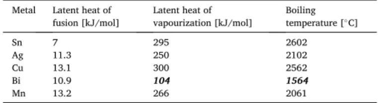
Table 1
Latent heat of fusion and vapourization of the different metals.
Metal Latent heat of
fusion [kJ/mol] Latent heat of
vapourization [kJ/mol] Boiling temperature [◦C]
Sn 7 295 2602
Ag 11.3 250 2102
Cu 13.1 300 2562
Bi 10.9 104 1564
Mn 13.2 266 2061
the latent heat of vapourization and boiling temperature are much lower. It means that the dissolved Bi needs much lower energy to reach the phase changes (vapourization and condensation as well) and leave the alloy than the other metals in our system.
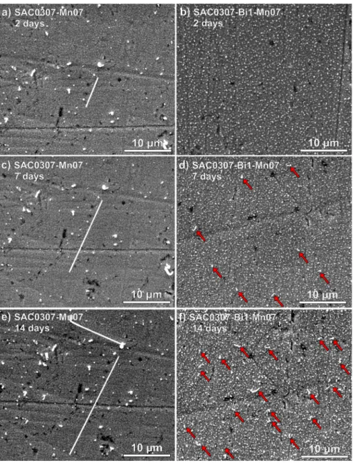
In the case of the SAC0307-Mn07 thin film layer, the whisker growth started directly after the layer deposition. Fig. 1a was done 30 min after the evaporation, and some nodule type whiskers were already found.
Fig. 3 shows the whisker growth in the same area with the same magnification (8000×) of the sample over the time of storing. The first filament type whiskers appeared on the SAC0307-Mn07 samples two days after the layer deposition, and the number of nodules was increased (Fig. 3a). The SAC0307-Bi1-Mn07 thin film layer still remained whisker free (Fig. 2b).
In seven days after the layer deposition, the whiskers appeared on the SAC0307-Bi1-Mn07 thin film layer (Fig. 3d), and the SAC0307- Mn07 thin film layer produced new ones as well (Fig. 3c). In the case of the SAC0307-Mn07 film layer, this tendency was going on until the 14th days when the whisker growth stopped (Fig. 3e). In the case of the
SAC0307-Bi-Mn07 thin film layer, the whisker formation continued until the end of the study (28 days). The whiskers on the SAC0307-Bi1- Mn07 thin film layer are barely observable due to the Bi grains, so the whiskers are marked by red arrows in Fig. 3. Generally, the filament type whiskers were rare during the study. Horv´ath [32] showed that the presence of other metals (like Cu or Ag) in the whisker bodies could cause the twisting of the whiskers, which results in the growth of nodule type whiskers. This phenomenon might be the root cause of the rela- tively high number of nodule type whiskers in our study since the alloying Cu, Ag, Bi, and Mn atoms could easily diffuse into the whisker body.
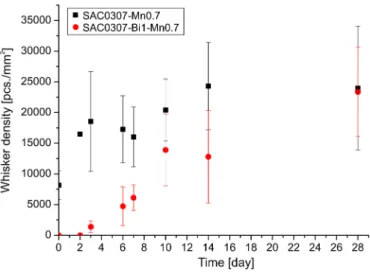
The in-depth statistical analyses supported the findings of the optical inspections (Fig. 4). On the SAC0307-Mn07 samples, the average whisker density was ~8.000 pcs/mm2 in half an hour after the layer deposition (Fig. 4).
In 3 days, the density increased to ~16.000 pcs/mm2 and did not change considerably then during the first week. After the 14th day, a further density increase occurred up to 24.000 pcs/mm2, which did not
Fig. 3. Whisker growth on the samples: a) SAC0307-Mn07, at 2 days after the deposition; b) SAC0307-Bi1-Mn07, at 2 days after the deposition; c) SAC0307-Mn07, at 7 days after the deposition; d) SAC0307-Bi1-Mn07, at 7 days after the deposition; e) SAC0307-Mn07, at 14 days after the deposition; f) SAC0307-Bi1-Mn07, at 14 days after the deposition.
change significantly until the end of the study (28 days). The SAC0307- Bi-Mn07 thin film layer showed similar whisker growth characteristics with a three-day delay. The whisker density increased up to ~14.000 pcs/mm2 between the 3rd and 10th days of the study, and it did not change until the end of the 2nd week. Later, it started to increase again up to 24.000 pcs/mm2 by 28 days. The typical length of the nodule whisker was between ~2 and 3 μm. The filament type whiskers were rare (~40 pcs/mm2), and they were found only on the SAC0307-Mn07 samples. Their typical length was between 10 and 25 μm. The longest detected filament whisker was only 41 μm long.
Comparing the results with previous researches [2,33,34], the number of formed whiskers was quite high in our present study. Vacuum evaporated Sn thin films with 400 nm, and 1 μm thickness produced only 3000–4000 pcs./mm2 whisker densities under laboratory conditions up to 28 days. Nevertheless, the ratio of filament type whiskers was much higher there, 195 pcs./mm2 [2,33]. In the case of ultra-thin Sn films, Crandall [34] has found 60–80 pcs of filament whiskers per mm2 on 75–100 nm thick layers under room conditions; however, she used magnetron sputtering for layer deposition, which could have resulted in a different layer structure. In this research, the ultra-thin film layer produced numerous whiskers due to the small grain size and mono-layer structure, which considerably decreased the relaxation ability of the layer. However, the Bi addition suppressed the formation of the dangerous filament-type whiskers. Their number was also lower in the case of the SAC0307-Mn07 alloy than in the case of pure Sn layers.
Although the deviations are very high and overlapping (Fig. 4), the averages suggested that the whisker growth happened in two “waves” in both cases. This phenomenon might be explained with the following effects: during the condensation of the solder alloy onto the Cu substrate, considerable IMC formation occurred, which caused immediate me- chanical stress in the ultra-thin film layers [35]. The ultra-thin film layers relieved this stress with the first wave of whisker growth. The second wave of whisker growth might be caused by further IMC growth in the solid-state of the thin film layers. This phenomenon also resulted in the consumption of the ultra-thin film layer and stopped the whisker growth after 14 and 28 days in the case of the SAC0307-Mn07 and SAC0307-Bi-Mn07 solder alloys, respectively. In the case of thicker Sn layers, the whisker growth happens in one wave [2,33]. Probably the first wave does not exist at all since the magnitude of the initial loading by the initial IMC formation during the layer deposition is lower.
However, the second wave generally lasts longer due to the larger amount of Sn in the layer [2,33].
The layer structure underneath the whiskers was investigated in FIB cuts to prove the previous preconception about the IMC growth and whisker formation. Fig. 5 shows the SAC0307-Mn layer under a
filament- and a nodule-type whiskers at 28 days after the layer deposi- tion. It is visible that the layer thickness was also in the range of 100–150 nm in the case of SAC0307 alloy (Fig. 5b and c.).
The formation of Cu6Sn5 IMC consumed most of the SAC0307-Mn0.7 layer during the 28 days of the test. The IMC layer is already visible from the upside of the thin-film layer (Fig. 5b), so it reached the top of the thin-film layer at various places, and they can be found directly under the root of the whiskers (Fig. 5c). The grain size of the Cu6Sn5 particles is one order of magnitude finer than the grain size of the SAC0307-Mn0.7 layer (Fig. 5b and d) [35]. Since the IMC formation eventually consumed most of the thin-film layer by the end of the research period, it stopped the growth of whiskers because there is no continuous Sn source anymore for whisker formation. Significant differences were not found between the root of the filament- and nodule-type whiskers. The SAC0307-Mn07 solder alloy produced fewer filament-type whiskers, and they were also shorter than in the case of pure Sn thin film layers [2, 33]. Although the ultra-thin solder layer produced a lot of whisker due to mechanical stress by the IMC layer growth [36,37], the smaller amount of Sn (the ultra-thin film layer) could also limit the growth of longer whiskers, as it was found in Ref. [2].
During the detailed investigation of the whisker growth on the SAC0307-Bi1-Mn07 layer, the previously observed differences in in- tensity were also found with the SEM-BSE detector. Fig. 6a shows an interesting phenomenon, a part of the whisker body appeared slightly darker than the rest of the whisker body. The EDS spectra prove that the darker part of the whisker is composed of Sn (Fig. 6b, measurement point M1), but the rest of the whisker is more reach in Bi (Fig. 6c, measurement point M2). (The “x” marks the exact location where the EDS spectra were done.) This phenomenon was general in the case of the SAC0307-Bi1-Mn07 layer; a smaller portion of the whiskers was Sn, and a larger part was Bi. The EDS spectrum of the measurement point M3 (Fig. 6d) shows that the Cu6Sn5 layer reached the top of the SAC0307- Bi1-Mn07 layer during 28 days of the test, similarly to the case of the SAC0307-Mn07 layer.
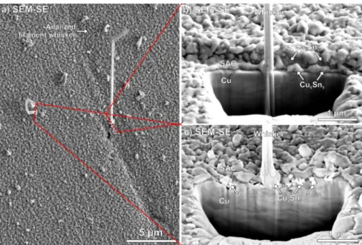
Fig. 7a shows two more examples of this unique Bi–Sn whisker couple phenomenon. The layer structure under the bigger nodule whisker was investigated in Fig. 7b. The cross-section of the whisker body proves that it is not one whisker but a shorter Sn and a longer Bi whisker next to each other, which grew from two neighbouring grains.
The red dotted line marks the grain boundary of the neighbouring Sn and Bi grains. Originally both grains were located on the Cu substrate.
The smaller grains of the Cu6Sn5 IMC particles are already visible be- tween the Sn and Bi grains [35], so the IMC formation consumed most of the SAC0307-Bi1-Mn0.7 layer during the 28 days of the test.
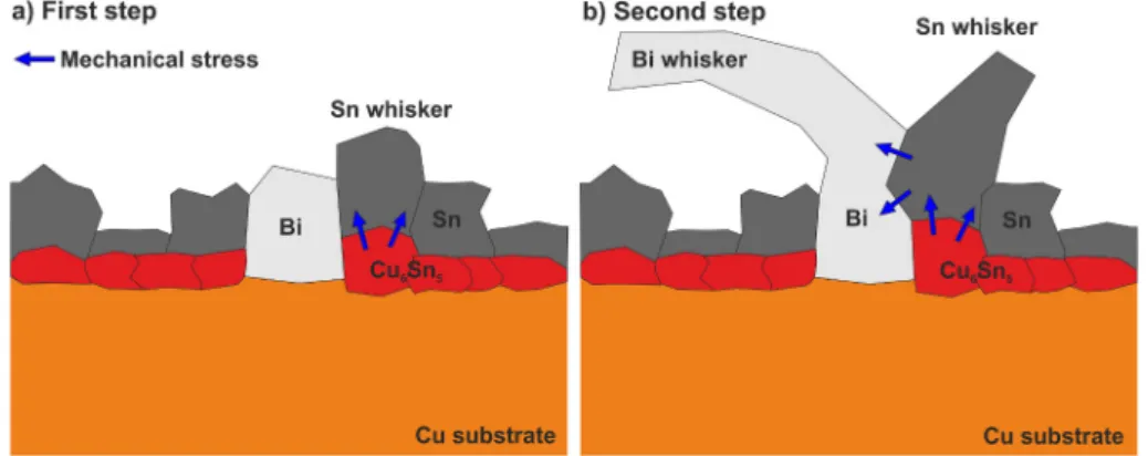
The possible growth mechanism of the Bi–Sn whisker couples can be seen in Fig. 8. (The thickness of the solder layer is distorted to the thickness of the Cu substrate.) The growth of the Cu6Sn5 particles causes mechanical stress on the Sn grains due to their expansion between the Sn grains [36]. The mechanical stress could reach even the range of 1–5 GPa for a while [37]. In the first step, the highly stressed Sn grains relieved the stress by whisker formation (Fig. 8a) and partially through grain boundary diffusion. At the same time, the growth of the stressed Sn grains started to load the neighbouring Bi grain in the mono-layer structure (one-grain thick layer), which also responded by whisker for- mation in the second step (Fig. 8b). The Bi whiskers were usually much longer than the neighbouring Sn ones. It might be explained by different mechanical parameters of the Bi. The Bulk modulus of the Sn and Bi is 58 GPa and 31 GPa, respectively. Therefore, the softer Bi could produce longer whiskers at a given stress level.
The addition of Bi to the SAC0307-Mn07 alloy suppressed the for- mation of filament-type whiskers. As it was reported, the Bi addition decreases the creep resistance of the SAC alloys [38]. The higher creep resistance of a pure SAC alloy may mean that mechanical stress is more readily transferred from the bulk layer to weaker parts of the overall structure (to roots of whiskers). Contrary, more creep-prone alloys (Bi-doped) can accommodate the stress within the more ductile layer Fig. 4. Average whisker densities.
itself. The evenly distributed, softer Bi grains in the Sn lattice also could aid in relieving the mechanical stress in the layer locally by Bi whisker formation. These previous effects might prohibit the filament-type whisker growth in the case of SAC0307-Bi1-Mn07 alloy. Similar re- sults have been found by Zhang et al. [39], who studied whisker growth in Ti2SnC/Sn-xBi system and found that Bi addition could suppress the filament whisker formation even at 100 ◦C heat annealing. However, at
125 ◦C [40] and 150 ◦C [39] the suppression effect decreased consid- erably. The appearance of nodule-type whiskers was considerable in both cases of the investigated alloys, but these whiskers do not cause reliability issues in microelectronic appliances due to their short length (2–3 μm). Consequently, the alloying of Mn and Bi into the high Sn content solders have a definite positive effect on their reliability from the whisker growth point of view.
Fig. 5. FIB cut of a filament and a nodule whisker on the SAC0307-Mn07 layer, at 28 days after the layer deposition: a) the analyzed filament and nodule whisker; b) layer structure under the filament whisker; c) layer structure under the nodule whisker.
Fig. 6. Whiskers on SAC0307-Bi1-Mn07 thin film layer at 28 days after the evaporation: a) SEM-BSE micrograph; b-d) EDS spectrum of the layer and a whisker.
4. Conclusions
The whisker growth from ultra-thin SAC0307-Mn07 and SAC0307- Bi1-Mn07 film layers were investigated in laboratory conditions. It was found that vacuum evaporation resulted in mono-layers, and in the case of the SAC0307-Bi1-Mn07 alloy, evenly distributed Bi grains formed in the ultra-thin film layer. The SAC0307-Mn07 started the whisker formation right after the layer deposition, while the SAC0307- Bi1-Mn07 layer started the whisker formation only three days after the layer deposition. Our hypothesis is that the Bi addition could decrease the Bulk modulus of the alloy; this effect and the separately formed Bi grains could increase the relaxing ability of the SAC0307-Bi1- Mn07 layer. In both cases, the whisker density reached very high numbers (~24 000 pcs./mm2), but most of the whiskers formed in the less critical nodule-type in morphology. The SAC0307-Mn07 alloy pro- duced ~40pcs/mm2 filament-type whisker with limited lengths, while the SAC0307-Bi1-Mn07 alloy suppressed the formation of filament-type whiskers. Furthermore, an interesting phenomenon was observed that the SAC0307-Bi1-Mn07 layer produced Bi–Sn whisker couples. Our hypothesis is that the appearance of the whisker couples might be caused by the mechanical stress transfer from the stressed Sn grain to the neighbouring Bi grain, which also reacted to the stress by whisker for- mation. Altogether the alloying of Mn and Bi into the high Sn content solders have positive effects on the reliability of microelectronics ap- pliances. It was proved that using thin-films for whisker studies is a fast and cost-effective method to obtain initial information about the whisker formation ability of a solder alloy. The obtained initial infor- mation could determine the direction of further researches on novel solder alloys, and it could help to understand the whisker phenomenon more deeply.
Declaration of competing interest
The authors declare that they have no known competing financial
interests or personal relationships that could have appeared to influence the work reported in this paper.
Acknowledgment
This research has been supported by the “TKP2020, Institutional Excellence Program” of the National Research Development and Inno- vation Office in the field of Nanotechnology and Materials Science (<u>BMEIE-NATTKP2020</u>).” and by the project
“<u>FK127970</u>” of the National Research Development and Innovation Office.
References
[1] W. Zhou, H. Zhang, P. Wu, Whisker growth in Sn and SnPb thin films under electromigration, Vacuum 107 (2014) 103–107, https://doi.org/10.1016/j.
vacuum.2014.04.010.
[2] B. Ill´es, T. Hurtony, O. Krammer, B. Medgyes, K. Dusek, D. Busek, Effect of Cu substrate roughness and Sn layer thickness on whisker development from Sn thin- films, Materials 12 (2019) 3609, https://doi.org/10.3390/ma12213609.
[3] D. Niraula, J. McCulloch, G.R. Warrell, R. Irving, V.G. Karpov, D. Shvydka, Electric field stimulated growth of Zn whiskers, AIP Adv. 6 (2016), 075201, https://doi.
org/10.1063/1.4955764.
[4] P. Zhang, J. Ding, Y. Liu, L. Yang, W. Tian, J. Ouyang, Y. Zhang, Z. Sun, Mechanism and mitigation of spontaneous Ga whisker growth on Cr2GaC, Sci. China Technol.
Sci. 63 (2020) 440–445.
[5] C. Lu, Y. Liu, J. Fang, Y. Zhang, P. Zhang, Z.M. Sun, Isotope study reveals atomic motion mechanism for the formation of metal whiskers in MAX phase, Acta Mater.
203 (2021) 116475, https://doi.org/10.1016/j.actamat.2020.11.017.
[6] Y. Liu, C. Lu, P. Zhang, J. Yu, Y. Zhang, Z.M. Sun, Mechanisms behind the spontaneous growth of Tin whiskers on the Ti2SnC ceramics, Acta Mater. 185 (2020) 433–440, https://doi.org/10.1016/j.actamat.2019.12.027.
[7] Y. Liu, P. Zhang, J. Yu, J. Chen, Y. Zhang, Z. Sun, Confining effect of oxide film on tin whisker growth, J. Mater. Sci. Technol. 35 (2019) 1735–1739, https://doi.org/
10.1016/j.jmst.2019.03.042.
[8] O. Krammer, T. Garami, B. Horv´ath, T. Hurtony, B. Medgyes, L. Jakab, Investigating the thermomechanical properties and intermetallic layer formation of Bi micro-alloyed low-Ag content solders, J. Alloys Compd. 634 (2015) 156–162, https://doi.org/10.1016/j.jallcom.2015.02.092.
Fig. 7.FIB cut of a nodule whisker on the SAC0307-Bi1-Mn07 layer, 28 days after the layer deposition: a) the analyzed nodule whisker; b) layer structure under the filament whisker.
Fig. 8. Growth mechanism of the Bi–Sn whisker couples.
[9] X. Zhong, L. Chen, B. Medgyes, Z. Zhang, S. Gao, L. Jakab, Electrochemical migration of Sn and Sn solder alloys: a review, RSC Adv. 7 (2017) 28186–28206, https://doi.org/10.1039/C7RA04368F.
[10] L.-W. Lin, J.-M. Song, Y.-S. Lai, Y.-T. Chiu, N.-C. Lee, Alloying design of Sn-Ag-Cu solders for the improvement in drop test performance, Proc. of IEEE 10th Electronics Packaging Technology Conference (2008) 33–36, https://doi.org/
10.1109/EMAP.2008.4784222.
[11] J.-M. Song, L.-W. Lin, N.-C. Lee, Y.-S. Lai, Y.-T. Chiu, Metallurgical perspective on alloying modification of Sn-Ag-Cu solders, Proc. of IEEE 10th Electronics Packaging Technology Conference (2008) 1358–1363, https://doi.org/10.1109/
EPTC.2008.4763620.
[12] L.-W. Lin, J.-M. Song, Y.-S. Lai, Y.-T. Chiu, N.-C. Lee, J.-Y. Uan, Alloying modification of Sn–Ag–Cu solders by manganese and titanium, Microelectron.
Reliab. 49 (2009) 235–241, https://doi.org/10.1016/j.microrel.2008.10.001.
[13] W. Liu, N.-C. Lee, A. Porras, M. Ding, A. Gallagher, A. Huang, S. Chen, J.C. Lee, Achieving high reliability low cost lead-free SAC solder joints via Mn or Ce doping, Proc. of IEEE Electronic Components and Technology Conference (2009) 994–1007, https://doi.org/10.1109/ECTC.2009.5074134.
[14] W. Liu, N.-C. Lee, A. Porras, M. Ding, A. Gallagher, A. Huang, S. Chen, J.C. Lee, Shock resistant and thermally reliable low Ag SAC solders doped with Mn or Ce, Proc. of IEEE 11th Electronics Packaging Technology Conference (2009) 49–63, https://doi.org/10.1109/EPTC.2009.5416572.
[15] A.A. El-Daly, A.M. El-Taher, S. Gouda, Development of new multicomponent Sn–Ag–Cu–Bi lead-free solders for low-cost commercial electronic assembly, J. Alloys Compd. 627 (2015) 268–275, https://doi.org/10.1016/j.
jallcom.2014.12.034.
[16] B. Ali, M.F.M. Sabri, S.M. Said, N.L. Sukiman, I. Jauharia, M.H. Mahdavifard, Microstructural and tensile properties of Fe and Bi added Sn-1Ag-0.5Cu solder alloy under high temperature environment, Microelectron. Reliab. 82 (2018) 171–178, https://doi.org/10.1016/j.microrel.2018.01.015.
[17] M.H. Mahdavifard, M.F.M. Sabri, S.M. Said, S. Rozali, High stability and aging resistance Sn-1Ag-0.5Cu solder alloy by Fe and Bi minor alloying, Microelectron.
Eng. 208 (2019) 29–38, https://doi.org/10.1016/j.mee.2019.01.011.
[18] T.-H. Chuang, S.-F. Yen, Abnormal growth of tin whiskers in a Sn3Ag0.5Cu0.5Ce solder ball grid array package, J. Electron. Mater. 35 (2006) 1621–1627, https://
doi.org/10.1007/s11664-006-0208-8.
[19] L. Hua, C. Yang, Corrosion behavior, whisker growth, and electrochemical migration of Sn–3.0Ag–0.5Cu solder doping with in and Zn in NaCl solution, Microelectron. Reliab. 51 (2011) 2274–2283, https://doi.org/10.1016/j.
microrel.2011.06.023.
[20] T. Chuang, C.C. Chi, Effect of adding Ge on rapid whisker growth of Sn–3Ag–0.5Cu–0.5Ce alloy, J. Alloys Compd. 480 (2009) 974–980, https://doi.
org/10.1016/j.jallcom.2009.02.118.
[21] B. Ill´es, B. Horvath, Tin whisker growth from micro-alloyed SAC solders in corrosive climate, J. Alloys Compd. 616 (2014) 116–121, https://doi.org/
10.1016/j.jallcom.2014.07.103.
[22] B. Ill´es, T. Hurtony, B. Medgyes, Effect of current load on corrosion induced tin whisker growth from SnAgCu solder alloys, Corrosion Sci. 99 (2015) 313–319, https://doi.org/10.1016/j.corsci.2015.07.026.
[23] B. Ill´es, N. Feh´erv´ari, Relation between tin whiskering ability Sn/Ag/Cu solder alloys and current load, Proceedings of 38th IEEE-ISSE conference (2015) pp173–178, https://doi.org/10.1109/ISSE.2015.7247984.
[24] A.M. Delhaise, Z. Bagheri, S. Meschter, P. Snugovsky, J. Kennedy, Whisker Growth on Electronic Assemblies Soldered with Bi-containing, Pb-free Alloys, 2020, https://doi.org/10.1007/s11664-020-08544-6 in press.
[25] A.M. Delhaise, S. Meschter, P. Snugovsky, J. Kennedy, Z. Bagheri, Tin whisker formation on small outline transistors assembled using bismuth-containing lead- free solder alloys after long-term ambient temperature, high humidity storage Part 2: statistical analysis, ), Journal of Surface Mount Technology 33 (2020) 7–19.
[26] O. Oudat, V. Arora, E.I. Parsai, V.G. Karpov, D. iana Shvydka, Gamma- and x-ray accelerated tin whisker development, J. Phys. D Appl. Phys. 53 (2020) 495305, https://doi.org/10.1088/1361-6463/abb38d.
[27] M. Hartmanov´a, M. Jergel, J.P. Holgado, J.P. Espinos, Structure and
microstructure of EB-PVD yttria thin films grown on Si (111) substrate, Vacuum 85 (2010) 535–540, https://doi.org/10.1016/j.vacuum.2010.09.003.
[28] A. Mazumder, V.D. Kumar, S. Sethi, J. Mukherjee, Continuous monitoring of temperature of electron beam heated metal evaporation surface using controlled gas purge at viewing port in a vacuum chamber, Vacuum 161 (2019) 157–161, https://doi.org/10.1016/j.vacuum.2018.12.037.
[29] O. Krammer, B. Ill´es, R. B´atorfi, K. Duˇsek, Automatic characterization method for statistical evaluation of tin whisker growth, Microelectron. Reliab. 73 (2017) 14–21, https://doi.org/10.1016/j.microrel.2017.04.007.
[30] J. Liu, H. Wang, Z. Zhang, J. Chen, H. Su, L. You, X. Song, Cr2Sn3-Mn3Sn heterostructure nanowires synthesized by evaporation-deposition method, Mater.
Res. Express 6 (2019) 115046, https://doi.org/10.1088/2053-1591/ab4623.
[31] M. Aljarrah, S. Obeidat, R.H. Fouad, M. Rababah, A. Almagableh, A. Itradat, Thermodynamic calculations of the Mn–Sn, Mn–Sr and Mg–Mn–{Sn, Sr} systems, IET Sci. Meas. Technol. 9 (2015) 681–692, https://doi.org/10.1049/iet- smt.2013.0267.
[32] B. Horv´ath, Influence of copper diffusion on the shape of whiskers grown on bright tin layers, Microelectron. Reilab. 53 (2013) 1009–1020, https://doi.org/10.1016/
j.microrel.2013.03.008.
[33] B. Ill´es, A. Skwarek, R. B´atorfi, J. Ratajczak, A. Czerwinski, O. Krammer, B. Medgyes, B. Horv´ath, T. Hurtony, Whisker growth from vacuum evaporated submicron Sn thin films, Surf. Coating. Technol. 11 (2017) 216–222, https://doi.
org/10.1016/j.surfcoat.2017.01.011.
[34] E.R. Crandall, Factors governing tin whisker growth, first ed., Springer Theses, London, UK, 2013, p. 145, https://doi.org/10.1007/978-3-319-00470-9.
[35] R.Z. Hu, M.Q. Zeng, M. Zhu, Cyclic durable high-capacity Sn/Cu6Sn5 composite thin film anodes for lithium ion batteries prepared by electron-beam evaporation deposition, Electrochim. Acta 54/10 (2009) 2843–2850, https://doi.org/10.1016/
j.electacta.2008.11.021.
[36] B.Z. Lee, D.N. Lee, Spontaneous growth mechanism of tin whiskers, Acta Metall. 46 (1998) 3701–3714, https://doi.org/10.1016/S1359-6454(98)00045-7.
[37] W.J. Boettinger, C.E. Johnson, L.A. Bendersky, K.-W. Moon, M.E. Williams, G.
R. Stafford, Whisker and Hillock formation on Sn, Sn–Cu and Sn–Pb electrodeposits, Acta Mater. 53 (2005) 5033–5050, https://doi.org/10.1016/j.
actamat.2005.07.016.
[38] D. Witkin, Creep behavior of Bi-containing lead-free solder alloys, J. Electron.
Mater. 41 (2012) 190–203, https://doi.org/10.1007/s11664-011-1748-0.
[39] Y. Zhang, C. Lu, Y. Liu, P. Zhang, Z. Sun, The effect of Bi addition on the formation of metal whiskers in Ti2SnC/Sn-xBi system, Vacuum 182 (2020) 109764, https://
doi.org/10.1016/j.vacuum.2020.109764.
[40] J. Tang, P. Zhang, Y. Liu, C. Lu, Y. Zhang, W. He, W. Tian, W. Zhang, Z. Sun, Selective growth of tin whiskers from its alloys on Ti2SnC, J. Mater. Sci. Technol.
54 (2020) 206–210, https://doi.org/10.1016/j.jmst.2020.02.081.