Whisker Development from SAC0307-Mn07 Solder Alloy
Balázs Illés1), Réka Bátorfi1), Tamás Hurtony1), Olivér Krammer1), Gábor Harsányi1), Alena Pietrikova2), Agata Skwarek3)4) and Krzysztof Witek4)
1) Department of Electronics Technology, Budapest University of Technology and Economics, Budapest, Hungary
2) Department of Technologies in Electronics, Technical University in Košice, Košice, Slovakia
3) Department of Marine Electronics, Gdynia Maritime Unversity, Gdynia, Poland
4) Łukasiewicz Research Network - Institute of Electron Technology, Kraków, Poland billes@ett.bme.hu
Abstract: In this study, the whisker growth from SAC0307-Mn07 solder alloy was investigated. To get fast information, an ultra-thin film was vacuum evaporated from the examined solder alloy onto Cu substrates. The evaporated layer was ~100-150nm thick in average with the same grain size. The layers were kept at room temperature for 28 days. Whisker growth was monitored by scanning electron microscope with some days frequency, and the layer structure under the whisker was examined on focused ion beam cuts. The large mechanical stress on the Sn layer due to the intermetallic layer growth initiated the whisker growth right after the layer deposition. However, it stopped after 2 weeks since the intermetallic grains consumed the ultra-thin Sn layer. The whisker density was extremely high (~24000 pcs./mm2). Most of the whiskers were the short nodule and hillock type, which does not mean risk in microelectronics. Therefore, the alloying of Mn into the high Sn content solder alloys have a positive effect on the reliability of the solder joints.
1.INTRODUCTION
Sn whiskers are spontaneously growing surface eruptions on the pure tin and high tin content surface finishes and solder joints. Their dimensions depend on the type of the whisker (hillock, nodule, or filament); they are between 0.5-10 µm in thickness and 5-3000 µm in length [1]. Therefore, tin whiskers mean high-reliability risk in microelectronics, due to the possibility of short circuit formation.
The lead-free change of the electronics industry initiated the application of various types of high tin content alloys, like SAC305 and SAC405 [2-5]. One of the main aims of the recent solder
developments is to reduce the silver content of the alloys, which results in the further growth of tin content up to 98-99 wt%. It can increase the appearance of whisker caused failures.
The mostly applied low-silver content alloy is the SAC0307, which has the composition ~98.7- 99Sn0.3Ag0.7Cu wt%, sometimes other micro-alloyed elements (wt%<0.1) are also used, like Ni, Co, Sb, etc. [6]. Other researches tried to improve the mechanical properties of the SAC alloy with further alloying of Bi and Mn in a higher amount between 0.1–1 wt% [7, 8]. Lin et al. [9] reached significant mechanical improvement during drop tests in the case of low Ag content Sn-l.0Ag-0.5Cu alloys doped with Mn and Ti (0.15 and 0.5wt%). Alloying of Mn and Ti resulted in rougher eutectic structure and more refined pro-eutectic Sn since the transition metal elements formed Intermetallic Compounds (IMCs) during the solidification rather than being dissolved into the Sn matrix [10]. Liu et al. [11] got similar results in the case of SAC105 alloys doped with Mn or Ce.
Xiang et al. [12] investigated the wettability and IMC formation in the case of Sn-3.8Ag-0.7Cu solder alloys doped with 0.11-0.47 wt% Mn. They found that the Mn suppressed the Cu6Sn5 formation.
However, it decreased the wetting ability as well. Krammer and Hurtony [13] tried the explain the better mechanical properties of Mn alloyed SAC solders via examining the fine microstructure of Mn alloyed SAC0307 by selective electrochemical etching. They proved that precipitates with high Mn growth in the solder joints, which can affect the mechanical properties of the solder joints. Medgyes et al. [8] investigated the effect of Mn alloying in SAC0307 alloy on the Electrochemical Migration (ECM) phenomenon by water drop tests. Although they did not find evidence for the migration of Mn, but unfortunately, Mn content decreased the ECM resistance.
The Sn whisker development ability of the Mn content alloys was never investigated before. The Cu-Sn layer structure is very frequent in microelectronics. Unfortunately, it is very sensitive to whisker growth. It is caused by the Intermetallic Layer (IML) growth at the boundary layer, which causes mechanical stress on the tin layer. The thickness of the Sn layer is a crucial parameter. In the case of a thicker Sn layer (>10µm), the whisker development is slower, since more time is required for the IML to create the stress. In the same way, the Sn whisker development is very fast on submicron thick tin layers. Therefore the application of thin-films is a very fast and cost-effective method to test the whisker growth ability of different solder alloys. In this research, our goal was to study the whisker growth ability of SAC0307-Mn07 solder alloy from ultra-thin tin films on Cu substrate.
2.MATERIALS AND METHODS
For the experiments, SAC0307-Mn07 alloy was evaporated onto Cu plates by electron beam physical vapour deposition (EB-PVD) using a Balzers BA 510 vacuum evaporator. Before the layer deposition, the Cu plates were annealed at 200ºC for 3 hours (to relax the surface). Then the surface oxides were removed manually by series application of P600, P1200, and P4000 of SIC grinding papers in a crosshatched pattern. The surface of the plates was polished on a buffer wheel in two steps, first with 3 μm diamond suspension and then with 1 μm diamond suspension. The roughness of the Cu plates was measured by Alpha-Step 500 surface profiler; it was 180±15nm (without oriented scratches).
After the polishing process, the Cu plates were washed in IPA and were neutralized by ion bombardment directly in the evaporator. The evaporation was done in a high vacuum (10-3 Pa) with cathode heating current 100mA and acceleration voltage 7kV. The evaporation time was 10 minutes, and it resulted in ~100-150 nm thick layer in average with the same grain size (Fig. 1). The grain size and the layer thickness was determined on cross-sections. They were prepared by a Thermo Scientific Scios 2 Dual-Beam Focused Ion Beam (FIB). The evaporated layers contained some straight ditches and holes. The ditches were formed due to the scratches of the Cu substrate. The hole-like structures were formed due to the not totally even evaporation, which is usual in the case of evaporation of alloys.
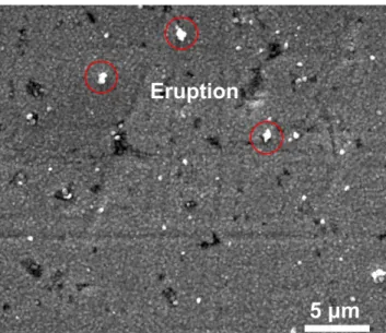
Fig. 1. SEM micrograph of the ultra-thin film layer directly after the deposition.
The samples were kept at room conditions for 28 days. The evaporated layers were inspected by a FEI Inspect S50 thermal emission-Scanning Electron Microscope (SEM), with some days frequency.
Surface cuts were prepared by Thermo Scientific Scios 2 Focused Ion Beam (FIB) to investigate the layer structure under the whiskers by a Thermo Scientific Scios 2 ultra-high resolution non-immersion field emission-SEM. Energy-dispersive X-ray Spectroscopy (EDS) analysis was used to identify the elemental compositions. Statistical parameters of the developed whiskers (density and length) were measured on SEM micrographs. The unit of the whisker density during the calculations was pcs./mm2. The axial length of the whiskers was measured according to the distance between the tip of the whisker and the surface, following the JESD201 standard. All statistics were calculated from 20 areas.
3.RESULTS AND DISCUSSIONS
The whisker development started directly after the layer deposition due to the considerable mechanical stress caused by the IML growth. Fig. 1 was done 30 mins after the evaporation, and some surface eruptions were already visible on the samples. First filament type whiskers appeared 2 days after the layer deposition (Fig. 2). However, most of the developed whiskers were hillock and nodule type (Fig. 3).
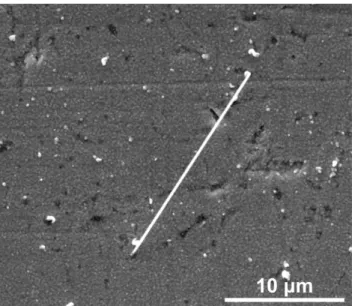
Fig. 2. Filament type Sn whisker (25μm long), 2 days.
The root cause of the relatively high number of hillock and nodule type whisker could be the thin Sn layer, which ensures the easy diffusion of Cu into the whisker bodies. The contamination can cause the formation of nodule type whiskers [14].
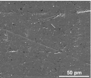
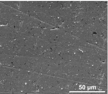
The following 3 SEM micrographs (Fig. 3-5) show the whisker growth at the same area of the sample in the function of time with 2000x magnification.
Fig. 3. Different types of Sn whiskers after 7 days.
Fig. 4. Different types of Sn whiskers after 14 days.
Fig. 5. Different types of Sn whiskers after 28 days.
The SEM micrographs show that whisker development was the most intense in the first half of the study (14 days), later no considerable change was visible in the number and in the size of the whiskers.
Statistical analyzes were conducted to get quantitative results about the previous findings.
The statistics supported the conclusions of the optical inspection. The average density of nodule and hillock type whiskers was ~ 8.000 pcs/mm2 half an hour after the layer deposition. In 2 days, it increased to ~16.000 pcs/mm2 and did not change during the first week. In the 2nd week, the density increased further up to 24.000 pcs/mm2 and did not change until the end of the study (28 days). Further researches are necessary to explain this fluctuating characteristic of whisker growth. The typical length of the nodule type whisker was only ~2-3 µm. The filament type whiskers were rare, only 40- 60 pcs/mm2 was found during the study. Their maximal length was also limited. It was between 10–
25 µm. The longest detected filament whisker was only 41µm.
Comparing the results with previous researches, the number of developed whiskers is extremely high [14, 15], which was probably caused by the very thin Sn layer. Here only 100–150 nm was applied contrary to the usual 0.5–2 µm. In the case of 1 and 2 µm thick Sn thin films, the average whisker densities were only 2900 and 70 pcs/mm2, respectively, after 4 weeks on ambient condition [14]. Probably here, the thinner Sn layer could relax less the stress caused by the IML growth. This assumption is supported by the observation that the whisker growth started directly after the layer deposition, while on the other cases, some days were required. However, the present study and the
referenced studies [14, 15] agree in the duration of new whisker growth. The appearance of new whiskers stopped or considerably slowed down 2 weeks after the layer deposition.
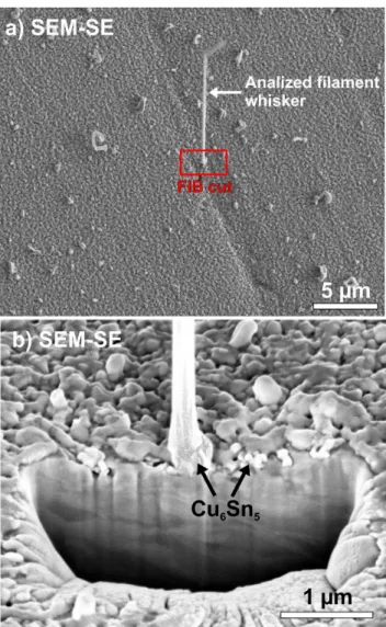
To prove our preconception about the IML growth, the layer structure under the whiskers were investigated. Fig 6 shows an analyzed filament type whisker, and the FIB cut under it, 28 days after the layer deposition. It is visible that the finer Cu6Sn5 grains already reached the top of the Sn layer. They can also be found under the root of the filament whisker. When the Cu6Sn5 grains migrated through the Sn layer, then the whisker growth stops, since there is no continuous Sn layer anymore, which could produce the whiskers.
In the case of ultra-thin film layers, it could occur in 1-2 weeks, that is why the whisker growth stops. However, in this 1-2 weeks, the mechanical stress is considerable on the ultra-thin film layer, which results in a lot of whiskers. Interestingly only a very few filament type ones. The few amounts of filament type whiskers could be caused by the alloying elements. Nodule type whisker formation can be initiated by contaminants inside the whisker, like alloying elements (such as Ag, Cu, Bi, etc.). If other elements get into the whisker body, it can result in the twisting of the whisker body and causes the growth of nodule type whiskers [14].
Fig. 6. FIB cut of a filament whisker, 28 days: a) the analyzed filament whisker; b) layer structure under the filament whisker.
It can be concluded that the Mn addition limited the filament whisker development effectively, in the number and in the maximal length too. Despite the very thin Sn layer, which could not relax the considerable mechanical stress of the IML growth. However, the few amounts of Sn (the very thin Sn layer) could also block the growth of longer whiskers, as it was found in [14]. The number of nodule and hillock type whiskers was very high. They cannot cause reliability problems in microelectronics due to their limited length (2-3µm). Therefore, the alloying of Mn into the high Sn content solder alloys have a positive effect on the reliability of the solder joints.
4.CONCLUSIONS
The whisker growth from SAC0307-Mn07 solder alloy was investigated in ultra-thin film form. The main findings are the following: the whisker development started already after the layer deposition, and most of the whisker developed in the first 2 weeks of the study. The whisker density was extremely high (~24000 pcs./mm2). However, most of the whiskers were the short nodule and hillock type (with only 2-3 μm length), which does not mean risk in microelectronics. It can be concluded that the Mn addition limited the filament whisker development effectively, in the number and in the maximal length too. Therefore, the alloying of Mn into the high Sn content solder alloys have a positive effect on the reliability of the solder joints. Further studies are necessary to test the whisker growth susceptibility of SAC-Mn alloys in the case of thicker Sn layers.
ACKNOWLEDGMENT
The research was organized partially in the frame of the Higher Education Excellence Program of the Ministry of Human Capacities, Nanotechnology and Materials Science research area of Budapest University of Technology and Economics (BME FIKP-NAT), in the frame of the National Research, Development and Innovation Office – NKFIH, FK 127970 and in the frame of Ministry of Science and Higher Education – Poland (MNiSW), project no 006/RID/2018/19 financed from the program
“Regionalna Inicjatywa Doskonałości 2019-2022”.
REFERENCES
[1] D. Bušek, J. Vávra, K. Dušek, “Whisker growth and its dependence on substrate type and applied stress”, Proc. of 2016 39th International Spring Seminar on Electronics Technology (ISSE), 2016, pp. 263-266.
[2] B. Kovács, A. Géczy, G. Horváth, I. Hajdu, L. Gál, “Advances in producing functional circuits on biodegradable PCBs”, Periodica Polytechnica Electrical Engineering and Computer Science, Vol.
60, 2016, pp. 223-231.
[3] Géczy2
[4] G.Á Farkas, P. Martinek, “Production plan scheduling on SMT manufacturing lines”, in proc. of IEEE 23rd International Symposium for Design and Technology in Electronic Packaging (SIITME), 2017, pp. 102-106.
[5] P. Veselý, E. Horynová, J. Starý, D. Bušek, K. Dušek, V. Zahradník, M. Plaček, P. Mach, M.
Kučírek, V. Ježek, M. Dosedla, "Solder joint quality evaluation based on heating factor", Circuit World, Vol. 44 No. 1, 2018 pp. 37-44.
[6] X. Zhong, L. Chen, B. Medgyes, Z. Zhang, S. Gao, L. Jakab, " Electrochemical migration of Sn and Sn solder alloys: a review ", RSC Advances, vol. 7, no. 45, 2017, pp. 28186-28206.
[7] P Tamási, G Kósa, B Szabó, R Berényi, B Medgyes, “Effect of Bismuth and Silver on the Corrosion behavior of Lead-free Solders in 3.5 wt% NaCl Solution”, Periodica Polytechnica Electrical Engineering and Computer Science, vol. 60, no 4, 2016, pp. 232-236.
[8] B. Medgyes, E. Roman, Á. Bohnert, S. Szurdán, X. Zhong, G. Harsányi, “Electrochemical migration investigations on SAC-Bi-xMn solder alloys”, in Proc. of IEEE 24th International Symposium for Design and Technology in Electronic Packaging (SIITME), 2018, pp. 80-83.
[9] L.-W. Lin, J.-M. Song, Y.-S. Lai, Y.-T. Chiu, N.-C. Lee, “Alloying Design of Sn-Ag-Cu Solders for the Improvement in Drop Test Performance”, Proc. of IEEE 10th Electronics Packaging Technology Conference, 2008, pp. 33-36.
[10] J.-M. Song, L.-W. Lin, N.-C. Lee, Y.-S. Lai, Y.-T Chiu, Metallurgical Perspective on Alloying Modification of Sn-Ag-Cu Solders, Proc. of IEEE 10th Electronics Packaging Technology Conference, 2008, pp. 1358-1363.
[11] W. Liu, N.-C. Lee, A. Porras, M. Ding, A. Gallagher, A. Huang, S. Chen, J. C. Lee, “Achieving High Reliability Low Cost Lead-Free SAC Solder Joints Via Mn or Ce Doping”, Proc. of IEEE Electronic Components and Technology Conference, 2009, pp. 994-1007.
[12] K. K. Xiang, A.S.M.A. Haseeb, M.M. Arafat, G. Yingxin, „Effects of Mn Nanoparticles on Wettability and Intermetallic Compounds in between Sn-3.8Ag-0.7Cu and Cu Substrate during Multiple Reflow”, Proc. of 4th Asia Symposium on Quality Electronic Design, 2012, pp. 297-301.
[13] O. Krammer, T. Hurtony, „Investigating the Fine Microstructure of Mn-doped SnAgCu Solder Alloys by Selective Electrochemical Etching”, Proc. of. 7th Electronic System-Integration Technology Conference (ESTC), 2018, pp. 1-5.
[14] B. Illés, T. Hurtony, O. Krammer, B. Medgyes, K. Dusek, D. Busek, “Effect of Cu substrate roughness and Sn layer thickness on whisker development from Sn thin-films”, Materials, vol. 12, 2019 p. 3609.
[15] B. Illés, A. Skwarek, R. Bátorfi, J. Ratajczak, A. Czerwinski, O. Krammer, B. Medgyes, B.
Horváth, T. Hurtony, “Whisker growth from vacuum evaporated submicron Sn thin films”, Surface and Coatings Technology, vol. 11, 2017, pp. 216-222.