The influence of the crystallographic structure of the intermetallic grains on tin whisker growth
Balázs Illés1),4), Agata Skwarek2),4), Jacek Ratajczak3), Karel Dušek4) and David Bušek4)
1) Department of Electronics Technology, Budapest University of Technology and Economics, Budapest, Hungary
2) Department of Microelectronics, Institute of Electron Technology, Krakow, Poland
3) Department of Materials and Semiconductor Structures Research, Institute of Electron Technology, Warsaw, Poland
4) Department of Electrotechnology, Czech Technical University in Prague, Prague, Czech Republic billes@ett.bme.hu
Abstract:
In this paper, the relationship between the crystallographic structure of Cu-Sn intermetallic grains and Sn whisker growth was investigated. In order to prevent the influence of the elements in the alloy composition and the effect of the soldering process on the formation of the intermetallic layer, 99.99%
pure Sn was vacuum evaporated onto Cu substrates. The Sn layer thickness was sub-micron region (~400nm in average) to reach considerable and rapid compressive stress on the tin layer originated by the intermetallic formation. The samples were stored at room temperature for 1 month. Different types of whiskers (nodule and filament) and the layer structure underneath were studied with a scanning ion microscopy and transmission electron microscopy. It was found that not only the thickness of the intermetallic layer and shape of the intermetallic grains affects the whisker growth but the crystallographic structure of the intermetallic grains as well. The susceptibility of the Sn layer to whisker development is higher in those regions where the intermetallic layer is composed of monocrystalline grains instead of those regions, where it is composed of polycrystalline grains. This effect can be explained by the higher compressive stress generated by the monocrystalline intermetallics compared to the polycrystalline ones.
KEY WORDS:tin whisker, intermetallic layer, crystallographic structure, TEM, thin film.
1.INTRODUCTION
Sn whiskers are surface eruptions [1] which can grow from high Sn content objects (like surface finishes and solder joints in microelectronic applications [2]). They can have mono- or polycrystalline structure and their usual dimensions are 1-10 µm in thickness and 10-500 µm in length. Sn whiskers present a reliability risk for microelectronic devices because they can form short circuits between the terminals of the components. Sn whisker growth is induced by compressive stress on the Sn layer such as direct external mechanical load (by mechanically closing connectors or test needles), residual stress by the Sn layer deposition [3], volumetric expansion by oxide and intermetallic development [4, 5], and thermomechanical effects [6]. The whisker development is a type of stress release mechanism for the tin layer against compressive stresses.
Besides compressive stresses, the physical parameters of the Sn layers (thickness, grain size and shape) [7] and the crystallographic structure (mono- or polycrystalline and the orientation) [8] has considerable effects on Sn whisker growth. The physical parameters of the Sn layer can be controlled with the deposition technology, namely electroplating, chemical (electro-less) technology and vacuum evaporation. Sn whisker development can be reduced and the incubation time can be increased by using a thick Sn layer (>10µm), since this configuration ensures better stress relaxation properties [9].
The influence of the grain size on whisker development is divided into two regimes. On one hand, small grains (<500nm) have more grain boundaries whereon electromigration causes higher diffusivity and results in fast intermetallic (IMC) layer growth [4, 10]. Sun et. al found that under a long-term mechanical load, dislocations can form at the Sn grain boundaries which produce a neighbouring grain; the new “twin boundary” can be the nucleation point of Sn whisker development [11]. On the other hand, small grains with a lot grain boundaries ensure better stress relaxation property of the Sn layer, like the increased Sn layer thickness.
The effect of the Sn grain shape is also related to whisker growth. Sauter et. al found that whisker development is reduced at globular/horizontal grain structure compared to columnar grain structure [12]. Yu et. al explained the phenomenon that wedge type intermetallics can from easily at the columnar grains (with straight grain boundaries) due to the predominance of grain boundary diffusion over bulk diffusion at lower temperatures, while this phenomenon does not occur at horizontal grains [13]. The crystallographic orientation of the grains also affects the Sn whiskering susceptibility [14, 15]. Jagtap et. al found whisker growth from the grains with low-index <100> or near-<100> grain orientation. The orientation of the nearest neighbours was also <100>, while the second nearest neighbours were high index planes, like <321> [16]. Eckold et. al found that in Sn layers the preferred
orientation of grains is <211>, because grains with such orientation have lower corrosion and tin whisker susceptibility than grains with <321> or <220> orientation [17]. However, Zhang et. al showed that bright Sn layers with a mixed <112> <101> <103> multi-peak texture also have low Sn whisker development susceptibility [18].
The Sn-Cu system can develop two types of intermetallics, Cu6Sn5 and the Cu3Sn. The Cu3Sn grows closer to the Cu in a less considerable amount compared to the Cu6Sn5, and Cu6Sn5 is located on the Cu3Sn towards Sn. The compressive stress due to volumetric expansion during IMC development (mainly the growth of the dominant Cu6Sn5) is one of the main sources that induces whisker development. Therefore, the different aspects of IMC development have already been investigated. It was shown that not only the amount and thickness of the IMC layer is important, but also the shape of the IMC grains. A greater tendency for whiskers development was found on non-uniform (rough) IMC layers [19, 20] and at larger IMC precipitates located between Sn grain boundaries [7]. From the point of the IMC layer development during the life cycle of the solder joints (in solid state), an important factor is the formation of the initial IMC layer during the soldering process (from the liquid state) [21]
or during the layer deposition process [22]. Zou et. al found that if the Cu concentration of the solder alloy is higher than the solubility, then the size of the IMC grains grows in proportion to the cube root of the reflow time [23]. The crystallographic structure of the Sn layer itself also has an effect on the IMC layer formation, since Tian et. al showed that the direction of c-axis in Sn grains affect the growth of the IMC, and that the IMCs in the solder matrix grew in the direction of the electron flow towards the c-axis direction [10].
Although the crystallographic structure of the IMC grains has already been investigated [24, 25], a correlation was not sought between the results and Sn whisker growth. Our hypothesis is that the crystallographic structure of the IMC grains affects the compressive stress generated by the IMC layer and via this affect the Sn whisker development as well.
2.EXPERIMENTAL PROCEDURE
Sn thin film on Cu substrate was selected as the material structure to be investigated. It has various advantages for our investigation. During our previous work, considerable tin whisker development was found on Sn thin films with a Cu substrate, only some days after the layer had been deposited [26]. In the submicronic (~400nm in average) Sn layer, the whiskering was induced solely by the rapid development of the Cu6Sn5 IMC layer, so the effect of surface oxidation on the whisker growth was
avoided. In addition, using vacuum evaporated Sn, the influences of the alloying elements and the soldering process on the formation of the IMC layer was also avoided. Therefore, 99.99% pure Sn was vacuum evaporated on Cu substrates as samples for the study.
The Sn layer was fabricated using the Electron Beam – Physical Vapour Deposition (EB-PVD) method with a Balzers BA 510 evaporator. Before the evaporation process, the Cu substrates were cleaned in isopropyl alcohol and were neutralized by ion bombardment. The settings of the evaporation process were as follows – cathode heating current 100 mA; acceleration voltage 7 kV;
high vacuum 10-3 Pa; and the evaporation time 25 min. The Sn layer was approximately 400nm in thickness and it was composed of ~1 µm size globular grains. The orientation (texture) of the deposited Sn thin film was generally <111>. The samples were stored at ambient laboratory temperature for 1 month and the whisker development was investigated using a FEI Inspect S50 Scanning Electron Microscope (SEM), (Acc. Voltage 20 kV).
The layer structure of the samples was studied on cross-sections prepared by a JEM-9320-FIB Focused Ion Beam (FIB) with Scanning Ion Microscopy (FIB-SIM), (with a 54° tilt angle, Ga Ion Source and Acc. Voltage of 30 kV). The lamellae for Transmission Electron Microscopy (TEM) analyses were prepared using the in-situ lift-out technique in the FIB system (FEI Helios NanoLab).
Before ion milling, the surface of the samples was covered with 80 nm thick dielectric SiO2 layer and 2 µm thick platinum layer to protect the top surface from damage by the high-energy gallium ion- beam. The lamellae were observed using a JEOL JEM-2100 (with LaB6 gun, Acc. Voltage 200kV).
Energy dispersive X-ray Spectroscopy (EDS) analysis was used to identify the elemental composition and distribution (EDS map) of the samples. The crystallographic structure of the grains was determined on electron diffraction patterns which were prepared using the Selected Area Electron Diffraction (SAED) technique.
3. RESULTS
After 1 month of samples storage, numerous tin whiskers were found (Fig. 1a). All of the whisker types (hillocks, nodules and filaments) were detected in large numbers with varying diameters and lengths. The longest detected filament type whiskers exceeded 300 µm. The average length of the filament type whiskers was around 80-100 µm, and in many cases they were near perpendicular to the surface (Fig. 1b). Nowadays, the minimal insulation distance used in microelectronics is 200 µm [27].
Therefore, the risk of short circuit formation is considerable in the case of submicron Sn layers on Cu
substrate. Fig. 2a) shows the Cu-Sn layer structure at two tin whiskers after 1 month of Sn film deposition. The results proved that the intensive IMC layer development caused the tin whisker growth. Furthermore, the IMC layer was usually thicker and rougher under the tin whiskers than at the areas free from whiskers. In order to investigate the crystallographic structure of the IMC grains, the Cu-Sn layer structure at the nodule and filament type whiskers (shown in Fig. 2b) was also investigated using TEM.
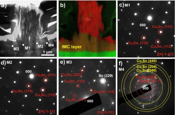
Fig. 3 shows the TEM analysis of a nodule type whisker (S1) and the Cu-Sn layer underneath. The EDS map (Fig. 3b) shows considerable IMC layer development between the Cu substrate and the Sn thin film. The SAED results of the IMC layer show that pure monocrystalline Cu6Sn5 grains were found with <111> orientation around the root of the whisker at the M1 and M2 measurement points (Fig. 3c-d). However, further from the whisker root, less Cu6Sn5 grains were found to be monocrystalline (see M3 measurement point, Fig. 3e). At measurement point M4 (Fig. 3f) the grains are already polycrystalline; here some Cu3Sn intermetallics were also found.
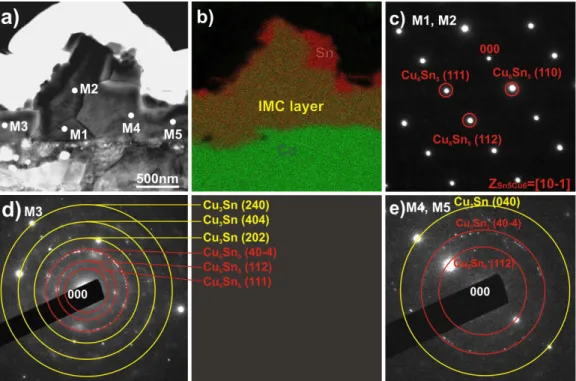
Fig. 4 shows the TEM analysis of another nodule type whisker (S2) and the Sn-Cu layer underneath. The IMC layer development was considerable here as well (Fig 4b), in addition, a large IMC precipitate was located directly under the whisker root. According to the SAED results, the upper region of the IMC layer – close to the whisker root – is formed from monocrystalline Cu6Sn5 grains (measurement points M1-M3, Fig. 4c-d) with <101> orientation. The presence of the pure Sn is still dominant with <111> orientation. Towards the Cu substrate, first the IMC grains are polycrystalline Cu6Sn5 (M4 measurement points (Fig. 4e), deeper into the layer they change to a mixture of polycrystalline Cu6Sn5 and Cu3Sn (M5 measurement point (Fig. 4f)).
Fig. 5 shows the TEM analysis of a 80µm filament type whisker (S3) and the Cu-Sn layer underneath. The structure of the IMC layer is very similar to the previous results (S1 and S2 whiskers).
Directly under the root of the whisker, the IMC layer is composed of monocrystalline Cu6Sn5 grains with the orientation <101> (M1 and M2 measurement points, Fig. 5c). Further from the whisker, the IMC layer contains a mixture of polycrystalline Cu6Sn5 and Cu3Sn intermetallics (M3-M5 measurement points, Fig 5d-e).
Fig. 6 shows the TEM analysis of a 20µm filament type whisker (S4) and the Cu-Sn layer underneath. The structure of the IMC layer follows the previous schema. Close to the whisker root, the IMC grains are monocrystalline and at the M1 measurement point (Fig 6b) both intermetallics are visible in one SAED measurement. The Cu6Sn5 grain has <011> orientation and the Cu3Sn grain has
<001> orientation. Towards the Cu substrate (M2 measurement point, Fig. 2c), at ~150µm deeper measuring location, only the Cu3Sn is visible. Further from the whisker, the IMC grains are polycrystalline and the mixture of the Cu6Sn5 and Cu3Sn intermetallics (M3-M6 measurement points, Fig 5d-f).
4.DISCUSSION
The development of the IMC layer is caused mainly by the diffusion of Cu atoms into Sn grains, which form intermetallic compounds within the grain boundaries. The most observed IMC compound was Cu6Sn5, which has lower density (8.27g/cm3) than copper (8.96g/cm3). This causes volume expansion at the IMC layer, which results in compressive stress on the Sn layer [20]. This compressive stress can be calculated [28]:
EIMC V V σ ∆
υ
= ⋅
−
1 (1)
where EIMC is the Young’s modulus of the intermetallics [Pa], υ is the velocity of the volume expansion [m/s] and V is the volume [m3]. The literature is not consistent about the Young’s modulus of Cu6Sn5, values can be found between ~50–150GPa depending on the type of measurement (nanoindentation or non-destructive ultrasonic technique) and on the type of the sample (casted bulk or developed by solid-state diffusion into a film layer) [29, 30].
This high variation of the values is probably due to the high anisotropic mechanical behaviour of the Cu6Sn5. Direct and indirect evidence for this phenomenon has been observed in former studies.
Vlassak and Nix investigated the elastic modulus of Cu by indentation, which has a cubic crystal structure. They found that Young’s modulus are 10–25% larger along the orientation <111> than along
<100>. The hexagonal structure of Cu6Sn5 allows us to assume that elasticity anisotropy in Cu6Sn5
would be even higher than in cubic Cu [31]. This assumption is supported by the results of An et al;
they found 30-70% variation of the Young’s modulus in Au5Sn and AuSn intermetallics, which materials also have non-cubic crystal structure [32]. Marques et al. investigated IMC layers developed from solid-state diffusion in Sn–Ag–Cu/Cu joints. They showed that the Young’s modulus of the Cu6Sn5 can vary by 14% when the indentations on the Cu6Sn5 are normal or parallel to the metallization plane [33]. Ghosh and Asta compared the Young’s modulus of bulk and film type Cu6Sn5
and found values of 84 to 102 GPa and 108 to 119 GPa respectively, although the effect of the texture on elasticity anisotropy was not investigated [34]. Deng et al. also measured higher Young’s modulus
in IMC layers formed during reflow soldering than in bulk IMCs [30]. Their explanation was that the casting technology of bulk intermetallics results in a polycrystalline intermetallic with relatively fine grain size, while the solid-state development of Cu6Sn5 in the reaction layer between the Sn and Cu usually results in monocrystalline intermetallic with orientation <102> or <101>, (due to the behaviour of one-dimensional diffusion profiles in a hexagonal structure) [35].
In film type monocrystalline Cu6Sn5, Young’s modulus values are usually reported to be larger than in the bulk polycrystalline Cu6Sn5, where the average is ~85.6 GPa [36]. Ostrovskaya et al.
investigated a similar vacuum deposited Sn-Cu layer on a beam. They calculated the Young’s modulus according to the change in the resonance frequency of the beam due to the Sn-Cu layer, and obtained 102GPa for Cu6Sn5. The exact growth orientation of the intermetallics was not reported [37]. Chromik et al. prepared Cu6Sn5 intermetallics by solid-state annealing of diffusion couples prepared from Cu substrate and Sn-Ag-Cu solder alloys. The Young’s modulus of Cu6Sn5 was 119 GPa [38]. Deng et. al reported 134.2±6.7GPa Young’s modulus values of Cu6Sn5 intermetallics, measured in situ in a solder joint using nanoindentation [39]. The previous results explain the great variation of the Young’s modulus in the literature. It can be assumed that the lower values in monocrystalline Cu6Sn5 originated from the presence of particular crystallographic orientations to the direction of indentation, while the higher values of the interfacial Cu6Sn5 come from its preferred growth orientation. Similarly, polycrystalline Cu6Sn5 has an intermediate Young’s modulus due to the averaging of the different orientations in the polycrystalline structure.
In our present study, correlation was found between the crystallographic structure of the Cu6Sn5
IMC grains and Sn whisker formation. Close to the Sn whisker roots, monocrystalline Cu6Sn5 grains were found., while further from the whisker roots they are usually polycrystalline. This effect might be caused by the higher Young’s modulus of the monocrystalline Cu6Sn5 intermetallic with preferred orientation compared to the polycrystalline Cu6Sn5. Therefore, the compressive stress value can be much higher close to the monocrystalline grains with preferred orientations than close to the polycrystalline ones. However, further research is necessary due to the uncertainty about the exact Young’s modulus value of the monocrystalline Cu6Sn5. No correlation was found between the type of Sn whiskers and the crystallographic structure of the Cu6Sn5 IMC grains.
5.CONCLUSIONS
The relationship between the crystallographic structure of the Cu-Sn IMC grains and Sn whisker growth was investigated in the case of vacuum evaporated Sn layers on Cu substrates. The high compressive stress of volume expansion during the Cu6Sn5 IMC layer development resulted in numerous Sn whiskers directly after the Sn layer deposition. All of the whiskers types (hillocks, nodules and filaments) were detected. The longest detected filament whiskers exceeded 300 µm, which means a reliability risk for microelectronics applications. The TEM investigation showed that not only the thickness of the IMC layer and the shape of the Cu6Sn5 grains affect Sn whisker development, but also the crystallographic structure of the IMC grains. Close to the Sn whisker roots, monocrystalline Cu6Sn5 grains were found., while further from the whisker roots they are usually polycrystalline. This phenomenon might be explained by the high elastic anisotropy of the Cu6Sn5 intermetallic. According to the literature, the Young’s modulus of the monocrystalline Cu6Sn5 intermetallic with preferred orientation can be much higher than the Young’s modulus of the polycrystalline Cu6Sn5. However, the literature is not straightforward about the Young’s modulus value of monocrystalline Cu6Sn5. Therefore, further research into this question is necessary.
6.ACKNOWLEDGEMENT
The research reported in this paper was partially supported by the Higher Education Excellence Program of the Ministry of Human Capacities in the frame of Nanotechnology and Materials Science research area of Budapest University of Technology and Economics (BME FIKP-NAT) and by the National Research, Development and Innovation Office – NKFIH, FK 127970.
REFERENCES
[1] A. Skwarek, J. Ratajczak, A. Czerwiński, K. Witek, J. Kulawik, Effect of Cu addition on whiskers formation in tin-rich solder alloys under thermal shock stress, Appl Surf Sci 255 (2009) 7100-7103 [2] D. Seehase, C. Kohlen, A. Neiser, A. Novikov, M. Nowottnick, Selective Soldering on Printed
Circuit Boards with Endogenous Induction Heat at Appropriate Susceptors, Period Polytech Electr Eng Comput Sci 62 (2018) 172–180.
[3] A. Sharma, S. Das, K. Das, Effect of different electrolytes on the microstructure, corrosion an whisker growth of pulse plated tin coatings, Microelectron Eng 170 (2017) 59–68.
[4] L. Ma, Y. Zuo, S. Liu, F. Guo, A. Lee, K.N. Subramanian, Whisker growth behaviors in POSS- silanol modified Sn3.0Ag0.5Cu composite solders, J Alloy Compd 657 (2016) 400–407.
[5] M.A. Ashworth, G.D. Wilcox, R.L. Higginson, R.J. Heath, C. Liu, R.J. Mo, The effect of electroplating parameters and substrate material on tin whisker formation, Microelectron Reliab 55 (2015) 180–191.
[6] A. Géczy, M. Fejős, L Tersztyánszky, Investigating and compensating printed circuit board shrinkage induced failures during reflow soldering, Solder Surf Mt Tech 27 (2015) 61-68.
[7] B. Illés, B. Horváth, Whiskering Behaviour of Immersion Tin Surface Coating, Microelectron Reliab 53 (2013) 755-760.
[8] P. Sarobol, J.E. Blendell, C.A. Handwerker, Whisker and hillock growth via coupled localized Coble creep, grain boundary sliding, and shear induced grain boundary migration, Acta Mater 61 (2013) 1991–2003.
[9] B. Horváth, B. Illés, T. Shinohara, G. Harsányi, Whisker Growth on Annealed and Recrystallized Tin Platings, Thin Solid Films 520 (2012) 5733-5740.
[10] Y. Tian, J. Han, L. Ma, F. Guo, The dominant effect of c-axis orientation in tin on the electromigration behaviors in tricrystal Sn-3.0Ag-0.5Cu solder joints, Microelectron Reliab 80 (2018) 7–13
[11] M. Sun, M. Dong, D. Wang, H. Ling, A. Hu, M. Li, Growth behavior of tin whisker on SnAg microbump under compressive stress, Scripta Mater 147 (2018) 114–118
[12] L. Sauter, A. Seekamp, Y. Shibata, Y. Kanameda, H. Yamashita, Whisker mitigation measures for Sn-plated Cu for different stress tests, Microelectron Reliab 50 (2010) 1631-1635.
[13] C.-F. Yu, C.-M. Chan, K.-C. Hsieh, The effect of tin grain structure on whisker growth, Microelectron Reliab 50 (2010) 1146–1151.
[14] W.J. Choi, T.Y. Lee, K.N. Tu, N. Tamura, R.S. Celestre, A.A. MacDowell, Y.Y. Bong, L.
Nguyen, Tin whiskers studied by synchrotron radiation scanning X-ray micro-diffraction, Acta Mater 51 (2003) 6253–6261.
[15] J. Stein, U. Welzel, A. Leineweber, W. Huegel, E.J. Mittemeijer, The crystallographic growth directions of Sn whiskers, Acta Mater 8 (2015) 102–109.
[16] P. Jagtap, A. Chakraborty, P. Eisenlohr, P. Kumar, Identification of whisker grain in Sn coatings by analysing crystallographic micro-texture using electron back-scatter diffraction, Acta Materialia 134 (2017) 346-359.
[17] P. Eckold, M.S. Sellers, R. Niewa, W. Hügel, The surface energies of β-Sn — A new concept for corrosion and whisker mitigation, Microelectron Reliab 55 (2015) 2799–2807
[18] W. Zhang, J. Guebey, M. Toben, A novel electrolyte for the high speed electrodeposition of bright pure tin at elevated temperatures, Metal Finish 109 (2011) 13-19.
[19] H.P. Lim, A. Ourdjini, T.A.A. Bakar, T. Tesfamichael, The effects of humidity on tin whisker growth by immersion tin plating and tin solder dipping surface finishes, Procedia Manufacturing 2 (2015) 275–279.
[20] K.S. Kim, C.H. Yu, S.W. Han, K.C. Yang, J.H. Kim, Investigation of relation between intermetallic and tin whisker growths under ambient condition, Microelectron Reliab 48 (2008) 111–118.
[21] M. Yang, Y. Cao, S. Joo, H. Chen, X. Mac, M. Li, Cu6Sn5 precipitation during Sn-based solder/Cu joint solidification and its effects on the growth of interfacial intermetallic compounds, J Alloy Compd 582 (2014) 688–695.
[22] B. Horváth, B. Illés, T. Shinohara, Growth of intermetallics between Sn/Ni/Cu, Sn/Ag/Cu and Sn/Cu layered structures, Thin Solid Films (2014) 345-353.
[23] H.F. Zou, H.J. Yang, Z.F. Zhang, Coarsening mechanisms, texture evolution and size distribution of Cu6Sn5 between Cu and Sn-based solders, Mater Chem Phys 131 (2011) 190–198.
[24] J. Gong, C. Liu, P.P. Conway, V.V. Silberschmidt, Evolution of CuSn intermetallics between molten SnAgCu solder and Cu substrate, Acta Mater 56 (2008) 4291–4297
[25] Z. Zhang, H Cao, M. Li, Y. Yua, H. Yang, S. Yang, Three-dimensional placement rules of Cu6Sn5 textures formed on the (111)Cu and (001)Cu surfaces using electron backscattered diffraction, Mater Design 94 (2016) 280–285
[26] B. Illés, A. Skwarek, R. Bátorfi, J. Ratajczak, A. Czerwinski, O. Krammer, B. Medgyes, B.
Horváth, T. Hurtony, Whisker growth from vacuum evaporated submicron Sn thin films, Surf Coat Tech (2017) 216-222
[27] O. Krammer, L.M. Molnár, L. Jakab, A. Szabó, Modelling the effect of uneven PWB surface on stencil bending during stencil printing process, Microelectron Reliab 52 (2012) 235-240.
[28] W.J. Boettinger, C.E. Johnson, L.A. Bendersky, K.-W. Moon, M.E. Williams, G.R. Stafford, Whisker and Hillock formation on Sn, Sn–Cu and Sn–Pb electrodeposits, Acta Mater 53 (2005) 5033–5050
[29] H. Rhee, J.P. Lucas, K.N. Subramanian, Micromechanical characterization of thermomechanically fatigued lead-free solder joints, J. Mat. Sci.: Mat Electron. 13 (2002) 477-484.
[30] X. Deng, N. Chawla, K.K. Chawla, M. Koopman, Deformation behavior of (Cu, Ag)–Sn intermetallics by nanoindentation, Acta Mater 52 (2004) 4291–4303
[31] J.J. Vlassak, W.D. Nix, Measuring the elastic properties of anisotropic materials by means of indentation experiments, J Mech Phys Solids 42/8 (1994) 1223-1245.
[32] R. An, C. Wang, Y. Tian, Depiction of the Elastic Anisotropy of AuSn4 and AuSn2 from First-
principles Calculations, Proc. ICEPT-HDP 2009:611–616.
http://dx.doi.org/10.1109/ICEPT.2009.5270675.
[33] V.M.F. Marques, C. Johnston, P.S. Grant, Nanomechanical characterization of Sn–Ag–Cu/Cu joints—Part 1: Young’s modulus, hardness and deformation mechanisms as a function of temperature, Acta Mater 61 (2013) 2460–2470
[34] G. Ghosh, M. Asta, Phase Stability, Phase Transformations, and Elastic Properties of Cu6Sn5: Ab initio Calculations and Experimental Results, J Mater Res 20/11 (2005) 3102-3117.
[35] K. H. Prakash, T. Sritharan, Effects of solid-state annealing on the interfacial intermetallics between tin-lead solders and copper, J Electron Mater 32 (2003) 939–947.
[36] A.-K. Larsson, L. Stenberg, S. Lidin, The superstructure of domain-twinned η-Cu6Sn5, Acta Crystallogr B 50 (1994) 636-643.
[37] L. M. Ostrovskaya, V. N. Rodin, A. I. Kuznetsov, Sov J Non-Ferrous Metals 26 (1985) 90-95 [38] R. R. Chromik, R. P. Vinci, S. L. Allen, M. R. Notis, Nanoindentation measurements on Cu–Sn
and Ag–Sn intermetallics formed in Pb-free solder joints, J Mater Res 18/9 (2003) 2251-2261 [39] X. Deng, M. Koopmanb, N. Chawla, K.K. Chawla, Young’s modulus of (Cu, Ag)–Sn
intermetallics measured by nanoindentation, Mat Sci Eng A-Struct 364 (2004) 240–243
List of figures:
Fig. 1. SEM micrograph of Sn whiskers, after 1 month of storage at room temperature: a) numerous varied Sn whiskers; b) a filament whisker more than 100µm long points out from the surface.
Fig. 2. SIM micrograph of Sn whiskers after 1 month of storage at room temperature: a) IMC layer formation under the whiskers; b) the whiskers investigated using TEM analyses.
Fig. 3. TEM analysis of a nodule whisker and the area underneath (S1): a) TEM bright field (BF) image; b) EDS element map; c)-f) TEM diffraction patterns at M1-M4 points.
Fig. 4. TEM analysis of a nodule whisker and the area underneath (S2): a) TEM bright field (BF) image; b) EDS element map; c)-f) TEM diffraction patterns at M1-M5 points
Fig. 5. TEM analysis of a filament whisker and the area underneath (S3): a) TEM bright field (BF) image; b) EDS element map; c)-e) TEM diffraction patterns at M1-M5 points.
Fig. 6. TEM analysis of a filament whisker and the area underneath (S4): a) TEM bright field (BF) image; b)-e) TEM diffraction patterns at M1-M6 points.