coatings
Article
Pulsed Laser Deposition of Aluminum Nitride Films:
Correlation between Mechanical, Optical, and Structural Properties
Lilyana Kolaklieva1, Vasiliy Chitanov1, Anna Szekeres2, Krassimira Antonova2,
Penka Terziyska2, Zsolt Fogarassy3, Peter Petrik3, Ion N. Mihailescu4and Liviu Duta4,*
1 Central Laboratory of Applied Physics, Bulgarian Academy of Sciences, 61 St. Petersburg Blvd., 4000 Plovdiv, Bulgaria; ohmic@mbox.digsys.bg (L.K.); vchitanov@gmail.com (V.C.)
2 Institute of Solid State Physics, Bulgarian Academy of Sciences, Tzarigradsko Chaussee 72, 1784 Sofia, Bulgaria; szekeres@issp.bas.bg (A.S.); krasa@issp.bas.bg (K.A.); penka@issp.bas.bg (P.T.)
3 Centre for Energy Research, Hungarian Academy of Sciences, Konkoly-Thegeút 29-33, H-1121 Budapest, Hungary; fogarassy.zsolt@energia.mta.hu (Z.F.); petrik.peter@energia.mta.hu (P.P.)
4 National Institute for Lasers, Plasma, and Radiation Physics, 409 Atomistilor Street, 077125 Magurele, Romania; ion.mihailescu@inflpr.ro
* Correspondence: liviu.duta@inflpr.ro
Received: 9 February 2019; Accepted: 13 March 2019; Published: 17 March 2019 Abstract: Aluminum nitride (AlN) films were synthesized onto Si(100) substrates by pulsed laser deposition (PLD) in vacuum or nitrogen, at 0.1, 1, 5, or 10 Pa, and substrate temperatures ranging from RT to 800◦C. The laser parameters were set at: incident laser fluence of 3–10 J/cm2 and laser pulse repetition frequency of 3, 10, or 40 Hz, respectively. The films’ hardness was investigated by depth-sensing nanoindentation. The optical properties were studied by FTIR spectroscopy and UV-near IR ellipsometry. Hardness values within the range of 22–30 GPa and Young’s modulus values of 230–280 GPa have been inferred. These values were determined by the AlN film structure that consisted of nanocrystallite grains, strongly dependent on the deposition parameters. The values of optical constants, superior to amorphous AlN, support the presence of crystallites in the amorphous film matrix. They were visualized by TEM and evidenced by FTIR spectroscopy. The characteristic Reststrahlen band of theh-AlN lattice with component lines arising from IR active phonon vibrational modes in AlN nanocrystallites was well detectable within the spectral range of 950–500 cm−1. Control X-ray diffraction and atomic force microscopy data were introduced and discussed. All measurements delivered congruent results and have clearly shown a correlation between the films’ structure and the mechanical and optical properties dependent on the experimental conditions.
Keywords: aluminum nitride; pulsed laser deposition; nanoindentation testing; TEM imaging;
FTIR spectroscopy; ellipsometry; complex refractive index
1. Introduction
Pulsed laser-assisted coatings represent a clean and fast route applied for surface modification and controlled micro-structuring of a wide range of materials. When compared to other physical vapor deposition methods, i.e., thermal evaporation or sputtering, pulsed laser deposition (PLD) stands out as a simple, versatile, rapid, and cost-effective method, which can enable precise control of thickness and morphology for the fabrication of high-quality thin films [1,2]. Amorphous or crystalline, extremely adherent, stoichiometric, dense, or porous structures from various complex materials can be synthesized, even at relatively low deposition temperatures, by simply varying the experimental
Coatings2019,9, 195; doi:10.3390/coatings9030195 www.mdpi.com/journal/coatings
Coatings2019,9, 195 2 of 16
parameters, mainly related to the (i) laser (fluence, wavelength, pulse-duration, and repetition rate) and (ii) deposition conditions (target-to-substrate distance, substrate temperature, nature, and pressure of the environment) [2–4].
Thin though hard coatings have proven invaluable for the production of mechanical parts or tools due to their hardness and wear-resistance characteristics [5,6]. In this respect, for the last couple of years, a great interest in using nitride-based films as protective coatings, due to their physical, chemical, electronic, thermal, or mechanical properties, has been reported [7–10]. In particular, aluminum nitride (AlN) coatings possess such characteristics, which make them suitable candidates for a wide range of applications, including insulating and buffer layers, photodetectors, light-emitting diodes, laser diodes, acoustic devices, or designs of self-sustainable opto- and micro-electronical devices [11–16].
Hard protective AlN coatings in multi-layered systems as AlN/TiN and CrN/AlN were intensively studied for tribological applications [8,9,17,18]. AlN is also commonly used in piezoelectric thin films [19,20], for the fabrication of micro-electro-mechanical system (MEMS) devices [21].
Depending on the deposition techniques and technological protocols, the AlN film structure can vary from fully-amorphous to nanocrystalline, with a tendency to decrease the volume fraction of grain boundaries [22–25]. This may significantly modify the physical, chemical, and mechanical properties of films with nano-sized crystalline structure in comparison to polycrystalline materials, which have grain sizes usually in the range of 100–300µm [26]. Highlyc-axis-oriented AlN films exhibit a large piezoelectric coefficient and are attractive for electroacoustic devices via surface acoustic waves [12,13].
Therefore, the fabrication of hard coatings based on properly-oriented nanocrystalline AlN layers requires a good understanding of their microstructure as a function of deposition conditions. However, obtaining AlN films with a definite structure and crystalline quality still remains a challenge for most deposition techniques. The PLD method has the main advantage of ensuring the growth of thin AlN films with good crystallinity and stoichiometry at relatively low temperatures [27]. Furthermore, PLD for AlN film synthesis proved to be one of the methods resulting in superior mechanical properties of the material [28]. There is still no straightforward theoretical or experimental model of the processes during deposition and the resulting film properties. Hence, the characterization of film growth and the mechanisms governing the film synthesis are important tasks in all application areas of AlN films.
Thin AlN films synthesis by the PLD technique is also the subject of our research. We focused during the years on the influence of the technological parameters, such as the assisting nitrogen gas pressure, incident laser fluence, repetition rate of laser pulses, substrate temperature, and the presence of an additional matching sub-layer, on the physical properties of AlN films synthesized by PLD [23,29–36] onto Si(100) substrates. Physical properties, such as surface roughness, microstructure, composition, amorphous-to-polycrystalline phase ratio, and optical constants appropriate for various applications, have been systematically studied. A systematization of the experimental results and finding the correlation between the structure and properties of the PLD AlN films and their preparation conditions would allow for the optimization of the deposition process in order to fabricate AlN films with the desired quality.
We resume with this paper the investigations with special attention to new, previously-unstudied phenomena, in the trial to better understand the quite complicated physical and chemical PLD process.
Thus, by depth-sensing nanoindentation, the mechanical properties of the PLD AlN films, fabricated at substrate temperatures ranging from room temperature (RT) up to 800◦C and, varying other deposition parameters such as ambient environment, gas pressure, laser incident fluence, and laser pulse frequency (LPF), were studied. Complementary results obtained by transmission electron microscopy (TEM), Fourier transform infrared (FTIR) spectroscopy, and UV-near IR ellipsometry are also reported, with the aim of finding the relationship between the structural properties of films and their mechanical properties.
Coatings2019,9, 195 3 of 16
2. Experimental Details
2.1. AlN Film Preparation
AlN films were synthesized onto Si(100) substrates by laser ablation of a polycrystalline stoichiometric AlN target using a pulsed KrF* excimer laser source COMPex Pro205 (Coherent, Göttingen, Germany,λ= 248 nm,νFWHM≤25 ns). The laser beam was oriented at 45◦with respect to the target surface. The laser pulse energy was ~360 mJ, and the incident laser fluence was set at ~3, 4, 4.8, or 10 J/cm2, respectively. The separation distance between the target and Si substrate was 5 cm.
The PLD process was performed in vacuum (~10−4Pa) or at different N2gas pressures of 0.1, 1, 5, or 10 Pa, respectively. Before each experiment, the irradiation chamber was evacuated down to a residual pressure of ~10−5Pa.
Prior to deposition, the Si substrates were cleaned in diluted (5%) hydrogen fluoride solution in order to eliminate the native oxide layer. The target was cleaned by baking at 800◦C for 1 h in a vacuum followed by a short multipulse laser ablation with 1000 pulses. A shutter was interposed in this case between the target and substrate to collect the expelled impurities.
During deposition, the target was continuously rotated with 0.4 Hz and translated along two orthogonal axes to avoid piercing and allow for the growth of uniform thin films. The substrate was heated either at 800, 450, 400, and 350◦C or was maintained at RT. The chosen temperature was kept constant with the help of a PID-EXCEL temperature controller (Excel Instruments, Gujarat, India).
For the deposition of one thin film, 15,000, 20,000, or 25,000 consecutive laser pulses were applied, with a corresponding LPF of 40, 10, or 3 Hz, respectively.
2.2. Nanoindentation Testing
The mechanical properties of the synthesized AlN films were investigated by a depth-sensing indentation method using Compact Platform CPX-MHT/NHT equipment (CSM Instruments/Anton-Paar, Peseux, Switzerland). Nanoindentation was performed with a triangular diamond Berkovich pyramid having a facet angle of 65.3◦±0.3◦(CSM-Instruments SA certificate B-N 41), in the loading interval starting from 5–100 mN. The nanohardness and elastic modulus were determined from the load/displacement curves applying the Oliver and Phar method [37].
2.3. Transmission Electron Microscopic Measurements
The structure of the PLD AlN films was investigated by transmission electron microscopy (TEM) and high-resolution transmission electron microscopy (HR-TEM) with a Philips CM-20 (Amsterdam, The Netherlands) operated at a 200-kV accelerating voltage and a JEOL 3010 (Tokyo, Japan) operated at a 300-kV accelerating voltage. The cross-sectional TEM samples were prepared by ion beam milling.
2.4. Optical Measurements
The influence of the deposition conditions on the films’ complex refractive index (ñ=n−jk, where nis the refractive index andkis the extinction coefficient) was studied by spectroscopic ellipsometry (SE) measurements on an M1000D ellipsometer from J.A. Woollam Co., Inc. (Lincoln, NE, USA) working in the spectral range of 193–1000 nm. In the SE data analysis, the Complete EASE J.A.
Woollam Co., Inc. software (version 5.08) was used [38]. The experimental SE spectra were taken at RT and different angles of light incidence of 60◦, 65◦, and 70◦. In data simulation, a two-layer optical model (substrate–1st layer (film bulk)–2nd layer (surface roughness)) was applied. In the spectral range of 400–1000 nm, the data were fitted by the Cauchy model to obtain the films’ thickness values.
The ellipsometric data were fitted by a Tauc–Lorentz general oscillator model. The surface roughness layer was modeled as a mixture of 50% material (film) and 50% voids (air) and was calculated by applying Bruggeman’s effective medium approximation theory.
FTIR reflectance spectra were obtained in a linearly-polarized incidence beam by using a Bruker Vertex 70 instrument (Billerica, MA, USA) equipped with a reflectance accessory A513/Q. Bothsandp
Coatings2019,9, 195 4 of 16
irradiation polarizations were exploited at an incident angle of 70◦. In this geometry, it is more correct to consider the orientation ofEwith respect to the normal to the film surfacezinstead of the optical nanocrystalline axisc, which could be oriented in a certain direction with a probability depending on the deposition conditions. Furthermore, it should be underlined that during every measurement, the components of the electric vectorEoriented along thex,y, andzdirections were presented with different weights at different temperatures. Thus, all electric field components contributed to the phonon-polariton modes in randomly-oriented AlN nanocrystallites. The spectral resolution was 2 cm−1, and the total number of scans per each measurement was 64.
3. Results and Discussion
3.1. Nanoindentation Testing
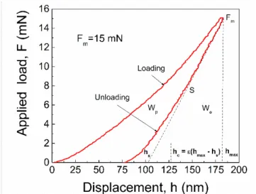
For all AlN films, the measured load-penetration depth curves with maximum indentation loads were smooth, with no discontinuities. The smooth loading nature testifies to the good film uniformity and adherence to the Si substrate. Even for the highest displacement load of 100 mN, when the indentation depth was close to the film thickness, there were no signs of cracking or peeling, which demonstrates the good interface quality. In Figure1, a typical load versus indenter displacement curve is presented, corresponding to a test performed on an AlN film deposited at 800◦C, in 0.1 Pa N2
pressure and at a LPF of 40 Hz. The main parameters used for the analysis are marked on the graph.
Fmis the peak load corresponding to a maximum nominal penetration depthhmax, which depends on the hardness and, consequently, on the film structure. The stiffnessSresults from the slope of the tangent to the unloading curve. The measured depthhverifies the relationh=hs+hc/ε, wherehsis the displacement of the surface at the perimeter of the contact,hcis the vertical distance along which the contact is made, andεis an indenter constant.
Coatings 2019, 9, x FOR PEER REVIEW 4 of 17
the deposition conditions. Furthermore, it should be underlined that during every measurement, the components of the electric vector E oriented along the x, y, and z directions were presented with different weights at different temperatures. Thus, all electric field components contributed to the phonon-polariton modes in randomly-oriented AlN nanocrystallites. The spectral resolution was 2 cm–1, and the total number of scans per each measurement was 64.
3. Results and Discussion
3.1. Nanoindentation Testing
For all AlN films, the measured load-penetration depth curves with maximum indentation loads were smooth, with no discontinuities. The smooth loading nature testifies to the good film uniformity and adherence to the Si substrate. Even for the highest displacement load of 100 mN, when the indentation depth was close to the film thickness, there were no signs of cracking or peeling, which demonstrates the good interface quality. In Figure 1, a typical load versus indenter displacement curve is presented, corresponding to a test performed on an AlN film deposited at 800 °C, in 0.1 Pa N2 pressure and at a LPF of 40 Hz. The main parameters used for the analysis are marked on the graph. Fm is the peak load corresponding to a maximum nominal penetration depth hmax, which depends on the hardness and, consequently, on the film structure. The stiffness S results from the slope of the tangent to the unloading curve. The measured depth h verifies the relation h = hs + hc/ε, where hs is the displacement of the surface at the perimeter of the contact, hc is the vertical distance along which the contact is made, and ε is an indenter constant.
Figure 1. Typical load-displacement curve at the maximum load of 15 mN in the case of an AlN film deposited at 800 °C, in 0.1 Pa N2 pressure and with a laser pulse frequency of 40 Hz.
The area between the loading and unloading curves defines the plastic deformation work Wp, while that between the unloading curve and perpendicular to the maximum penetration depth, hmax, is a measure of the elastic deformation work, We. The ratio We/(We + Wp) defines the elastic recovery of the coating after indentation and is associated with the coating ability to go back after deformation. For the studied films, this ratio varied from 49%–67%, depending on the deposition conditions. This implies a very good coating recovery after mechanical deformation.
The measured load and displacement curves were analyzed, and the nanohardness H and elastic modulus E were evaluated [37]. The hardness was estimated from the relation H = Fmax/A, where A is the projected contact area of the indentation. By fitting the unloading curve, i.e., the stiffness S = dF/dh, the projected area A can be determined. The Young’s modulus E is determined from the relation (1 − ν2)/E = (2A1/2/Sπ1/2) − (1−νi2)/Ei [37], where Ei and νi are the elastic modulus and Poisson’s ratio of the indenter (ν was assumed equal to 0.22).
Figure 1.Typical load-displacement curve at the maximum load of 15 mN in the case of an AlN film deposited at 800◦C, in 0.1 Pa N2pressure and with a laser pulse frequency of 40 Hz.
The area between the loading and unloading curves defines the plastic deformation workWp, while that between the unloading curve and perpendicular to the maximum penetration depth, hmax, is a measure of the elastic deformation work,We. The ratioWe/(We +Wp) defines the elastic recovery of the coating after indentation and is associated with the coating ability to go back after deformation. For the studied films, this ratio varied from 49–67%, depending on the deposition conditions. This implies a very good coating recovery after mechanical deformation.
The measured load and displacement curves were analyzed, and the nanohardnessHand elastic modulusEwere evaluated [37]. The hardness was estimated from the relationH=Fmax/A, where Ais the projected contact area of the indentation. By fitting the unloading curve, i.e., the stiffness
Coatings2019,9, 195 5 of 16
S= dF/dh, the projected areaAcan be determined. The Young’s modulusEis determined from the relation (1−ν2)/E= (2A1/2/Sπ1/2)−(1−νi2)/Ei[37], whereEiandνiare the elastic modulus and Poisson’s ratio of the indenter (νwas assumed equal to 0.22).
The dependence of the nanohardness and elastic modulus on the indentation depth corresponding to the applied load in the interval from 5–100 mN is presented in Figure2. Below the loading value of 5 mN, the hardness determination with sufficient accuracy is limited by the surface roughness [39].
Our PLD AlN films exhibited a considerably smooth and uniform surface morphology, with a root mean squared roughness in the range of 0.24–2.5 nm, depending on the deposition conditions [35,36,40].
Coatings 2019, 9, x FOR PEER REVIEW 5 of 17
The dependence of the nanohardness and elastic modulus on the indentation depth corresponding to the applied load in the interval from 5–100 mN is presented in Figure 2. Below the loading value of 5 mN, the hardness determination with sufficient accuracy is limited by the surface roughness [39]. Our PLD AlN films exhibited a considerably smooth and uniform surface morphology, with a root mean squared roughness in the range of 0.24–2.5 nm, depending on the deposition conditions [35,36,40].
Figure 2. Nanohardness H and elastic modulus E as a function of the maximum nominal penetration depth, hmax, of the PLD AlN films obtained using the deposition conditions given in the inset.
The variation of hardness with the indenter penetration depth points to a region of
∆hmax ≈ (150‒200) nm, corresponding to 10‒15 mN loading, where the H values of the films could be recorded with the weak influence of the Si substrate on the test measurements. With the further increase of the applied load, i.e., the increase of the maximum penetration depth, the nanohardness value dropped rapidly below 20 GPa, followed by a smooth decrease to values that approached the Si substrate hardness of ≈15 GPa. The latter implies an increasing influence of the substrate [41]. Taking the observed dependence into account, the further presented results correspond to the load of 15 mN, for which the influence of the Si substrate on the H values was similar. The observed variation of H values with substrate temperature can be assigned to a change in the microstructure of films. Elevated temperature facilitates the crystallization process, and thus, a less defective structure with a larger amount and size of h-AlN crystallite grain boundaries was growing, characterized by higher nanohardness values.
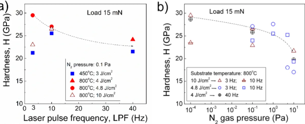
Our recent investigations on PLD AlN films have established that the variation of the nitrogen pressure, on one hand [23,30,33], and LPF, on the other [24,31,36], had the strongest influence on the formation of the AlN microstructure. The effect of laser incident fluence can be compensated by the variation of those two parameters. Correspondingly, in Figure 3, the H values are represented as a function of LPF (Figure 3a) and N2 pressure (Figure 3b) at other PLD parameters given in the insets. The AlN films were deposited under different conditions as either the N2 pressure was kept constant at 0.1 Pa while varying the laser fluence, LPF, and substrate temperature (Figure 3a) or the substrate temperature was kept at 800 °C (Figure 3b) while varying the nitrogen pressure, laser fluence, and LPF.
The observed hardness behavior is closely related to the processes of film growth and the resulting film microstructure, which yielded variation in the film hardness values. Nevertheless, all H values were within 22‒30 GPa range, superior to the ones registered in the case of films obtained by other deposition techniques [22,42–47].
Figure 2.NanohardnessHand elastic modulusEas a function of the maximum nominal penetration depth,hmax, of the PLD AlN films obtained using the deposition conditions given in the inset.
The variation of hardness with the indenter penetration depth points to a region of
∆hmax≈(150–200) nm, corresponding to 10–15 mN loading, where theHvalues of the films could be recorded with the weak influence of the Si substrate on the test measurements. With the further increase of the applied load, i.e., the increase of the maximum penetration depth, the nanohardness value dropped rapidly below 20 GPa, followed by a smooth decrease to values that approached the Si substrate hardness of≈15 GPa. The latter implies an increasing influence of the substrate [41].
Taking the observed dependence into account, the further presented results correspond to the load of 15 mN, for which the influence of the Si substrate on theHvalues was similar. The observed variation ofHvalues with substrate temperature can be assigned to a change in the microstructure of films.
Elevated temperature facilitates the crystallization process, and thus, a less defective structure with a larger amount and size ofh-AlN crystallite grain boundaries was growing, characterized by higher nanohardness values.
Our recent investigations on PLD AlN films have established that the variation of the nitrogen pressure, on one hand [23,30,33], and LPF, on the other [24,31,36], had the strongest influence on the formation of the AlN microstructure. The effect of laser incident fluence can be compensated by the variation of those two parameters. Correspondingly, in Figure3, theHvalues are represented as a function of LPF (Figure3a) and N2pressure (Figure3b) at other PLD parameters given in the insets.
The AlN films were deposited under different conditions as either the N2pressure was kept constant at 0.1 Pa while varying the laser fluence, LPF, and substrate temperature (Figure3a) or the substrate temperature was kept at 800◦C (Figure3b) while varying the nitrogen pressure, laser fluence, and LPF.
The observed hardness behavior is closely related to the processes of film growth and the resulting film microstructure, which yielded variation in the film hardness values. Nevertheless, allHvalues were within 22–30 GPa range, superior to the ones registered in the case of films obtained by other deposition techniques [22,42–47].
CoatingsCoatings 2019, 9, x FOR PEER REVIEW 2019,9, 195 6 of 166 of 17
Figure 3. Nanohardness as a function of laser pulse repetition frequency (a) and N2 gas pressure (b) for PLD AlN films deposited with variation of other PLD parameters (as given in the insets).
In general, a higher deposition temperature enhances the reaction at the surface of the substrate and promotes the formation of crystallites in the growing film [48]. As a result, AlN films deposited at 800 °C possessed higher hardness values (Figure 3a). When the deposition was performed at low N2 pressure, a high laser fluence of 10 J/cm2, and a low LPF of 3 Hz, the species evaporated from the polycrystalline AlN target acquired a much higher kinetic energy. This excess energy was transferred to adatoms when reaching the surface of the growing film, obstructing the ordering in a crystalline network. AlN films formed in these conditions were amorphous, as previously revealed by our TEM and XRD studies [23].
With increasing the LPF from 3 to 10 and 40 Hz, the multiple, consecutive vaporization “cleaned up” the space between the target and substrate. Consequently, the atoms ejected from the target had much more energy when reaching the substrate, contributing to the boost of the mobility of adatoms and surface diffusion. As one can observe in Figure 3a, the forming microstructure could be however more defective with lowered microhardness. When increasing the nitrogen pressure (Figure 3b), the particles ejected from the target in the plasma plume lost their energy in collisions with nitrogen particles. Accordingly, they could not significantly contribute to the thermally-induced mobility promoted by heating the substrate, but bound to their impinging sites without further surface migration. As a result, the formed film structure was less crystalline and more defective, which was reflected in the lower hardness values (Figure 3b).
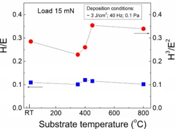
As known [49,50], the hardness and elastic modulus are important material parameters that indicate the resistance to elastic/plastic deformation and could be used for the estimation of the coating wear behavior. The H/E ratio characterizes the elastic strain to failure resistance, while the H3/E2 ratio evaluates the coating resistance to plastic deformation at sliding contact load. Both ratios are associated with the coating toughness, a key parameter for the evaluation of the tribological properties of materials [50]. Hence, the improvement of the tribological behavior can be achieved by increasing the coating hardness and decreasing the elastic modulus. In Figure 4, the resistance for elastic strain to failure (H/E) and to plastic deformation (H3/E2) of AlN films versus deposition temperature is presented.
Figure 3.Nanohardness as a function of laser pulse repetition frequency (a) and N2gas pressure (b) for PLD AlN films deposited with variation of other PLD parameters (as given in the insets).
In general, a higher deposition temperature enhances the reaction at the surface of the substrate and promotes the formation of crystallites in the growing film [48]. As a result, AlN films deposited at 800◦C possessed higher hardness values (Figure3a). When the deposition was performed at low N2pressure, a high laser fluence of 10 J/cm2, and a low LPF of 3 Hz, the species evaporated from the polycrystalline AlN target acquired a much higher kinetic energy. This excess energy was transferred to adatoms when reaching the surface of the growing film, obstructing the ordering in a crystalline network. AlN films formed in these conditions were amorphous, as previously revealed by our TEM and XRD studies [23].
With increasing the LPF from 3 to 10 and 40 Hz, the multiple, consecutive vaporization
“cleaned up” the space between the target and substrate. Consequently, the atoms ejected from the target had much more energy when reaching the substrate, contributing to the boost of the mobility of adatoms and surface diffusion. As one can observe in Figure3a, the forming microstructure could be however more defective with lowered microhardness. When increasing the nitrogen pressure (Figure3b), the particles ejected from the target in the plasma plume lost their energy in collisions with nitrogen particles. Accordingly, they could not significantly contribute to the thermally-induced mobility promoted by heating the substrate, but bound to their impinging sites without further surface migration. As a result, the formed film structure was less crystalline and more defective, which was reflected in the lower hardness values (Figure3b).
As known [49,50], the hardness and elastic modulus are important material parameters that indicate the resistance to elastic/plastic deformation and could be used for the estimation of the coating wear behavior. TheH/Eratio characterizes the elastic strain to failure resistance, while the H3/E2ratio evaluates the coating resistance to plastic deformation at sliding contact load. Both ratios are associated with the coating toughness, a key parameter for the evaluation of the tribological properties of materials [50]. Hence, the improvement of the tribological behavior can be achieved by increasing the coating hardness and decreasing the elastic modulus. In Figure4, the resistance for elastic strain to failure (H/E) and to plastic deformation (H3/E2) of AlN films versus deposition temperature is presented.
From the dependence of these ranking parameters, one can state that the studied PLD AlN films had a very highH3/E2ratio compared to other AlN coatings [43,44].
Coatings2019,9, 195 7 of 16
Coatings 2019, 9, x FOR PEER REVIEW 7 of 17
Figure 4. Resistance for elastic strain to failure (H/E) and plastic deformation (H3/E2) of the PLD AlN films as a function of substrate temperature during deposition.
From the dependence of these ranking parameters, one can state that the studied PLD AlN films had a very high H3/E2 ratio compared to other AlN coatings [43,44].
3.2. TEM Observations
Four types of significantly different AlN structures were revealed in previous TEM studies of PLD films [23,30,36]. Amorphous AlN layers are mostly forming at RT or in a growth environment where the mobility of the atoms after reaching the substrate surface is limited. When increasing the temperature, nano-sized crystalline grains in an amorphous matrix emerged. This case is well visible in Figure 5a, where the HR-TEM image of the AlN film, deposited at 450 °C, 0.1 Pa N2 pressure, LPF of 40 Hz, and incident laser fluence of 3 J/cm2, revealed hexagonal nanocrystallites surrounding with amorphous AlN. The reduced crystallinity was due to the relatively low substrate temperature of 450
°C. Here, AlN crystallites were hexagonal (h-AlN), but the metastable cubic (c-AlN) phase can also grow in the amorphous matrix [23,33,36]. The hardness of such AlN films may vary significantly due to the variation in the thickness of the amorphous matrix between the crystalline particles [51] and/or voids possibly incorporated into the layer, which may significantly reduce the film’s hardness.
The third type of AlN layer consists of columnar crystals with a highly crystalline h-AlN structure, mostly with the (001) texture [48]. A similar crystalline structure was observed for the AlN films grown at 800 °C. This is illustrated in Figure 5b, where the bright-field (BF) cross-sectional TEM image of AlN film deposited at 800 °C, 0.1 Pa N2 pressure, LPF of 40 Hz, and incident laser fluence of 3 J/cm2 is shown.
The columnar grains with a crystalline h-AlN structure are well seen. In the case of AlN films deposited at a higher temperature (800 °C), but in vacuum [23], a highly-ordered crystalline film structure was observed, where the h-AlN crystallites had grown epitaxially in a columnar orientation perpendicular to the Si substrate (Figure 6a,b). Although an epitaxial growth is achieved (as shown in Figure 6c), the layer is not a single crystal because h-AlN crystals grow with two preferred orientations, rotated from each other by 30° due to the growth of the h-AlN (001) plane onto the cubic Si lattice. The dark-field cross-sectional TEM image in Figure 6b was prepared from two dark-field images (separated from each other by color), which were recorded from spots with two possible epitaxial orientations. The selected area electron diffraction patterns in Figure 6c were taken from the cross-sectional TEM image in Figure 6a. In the first pattern (Figure 6c₁), the Si(100) substrate is shown, while the other two patterns (Figure 6c₂,c₃) show two possible epitaxially-oriented areas in the AlN film.
Figure 4.Resistance for elastic strain to failure (H/E) and plastic deformation (H3/E2) of the PLD AlN films as a function of substrate temperature during deposition.
3.2. TEM Observations
Four types of significantly different AlN structures were revealed in previous TEM studies of PLD films [23,30,36]. Amorphous AlN layers are mostly forming at RT or in a growth environment where the mobility of the atoms after reaching the substrate surface is limited. When increasing the temperature, nano-sized crystalline grains in an amorphous matrix emerged. This case is well visible in Figure5a, where the HR-TEM image of the AlN film, deposited at 450◦C, 0.1 Pa N2pressure, LPF of 40 Hz, and incident laser fluence of 3 J/cm2, revealed hexagonal nanocrystallites surrounding with amorphous AlN. The reduced crystallinity was due to the relatively low substrate temperature of 450◦C. Here, AlN crystallites were hexagonal (h-AlN), but the metastable cubic (c-AlN) phase can also grow in the amorphous matrix [23,33,36]. The hardness of such AlN films may vary significantly due to the variation in the thickness of the amorphous matrix between the crystalline particles [51] and/or voids possibly incorporated into the layer, which may significantly reduce the film’s hardness.
Coatings 2019, 9, x FOR PEER REVIEW 8 of 17
Figure 5. HR-TEM image of nano-sized crystalline grains in amorphous matrix (a) and bright field cross-sectional TEM image (b) of the PLD AlN films deposited at 450 and 800 °C, respectively. The other PLD parameters were identical: N2 pressure of 0.1 Pa, LPF of 40 Hz, and laser fluence of ≈3 J/cm2.
Figure 6. Bright-field (a) and dark-field (b) cross-sectional TEM images of the PLD AlN film deposited in vacuum (10−4 Pa) at a temperature of 800 °C, laser fluence of 10 J/cm2, and LPF of 3 Hz. In (c), the corresponding selected area electron diffraction (SAED) patterns from (a) are shown: SAED pattern of the Si(100) substrate (c₁) and SAED patterns of AlN films (c₂,c₃) taken from two possible epitaxially-oriented areas.
TEM observations correlated well with the results of our earlier studies of PLD AlN films by X-ray diffraction (XRD, Bruker Corporation, Billerica, MA, USA) [23,24,30,35,52]. Our analysis revealed that a stable h-AlN phase was forming with predominant (002) c-axis orientation, for films deposited at 450
Figure 5.HR-TEM image of nano-sized crystalline grains in amorphous matrix (a) and bright field cross-sectional TEM image (b) of the PLD AlN films deposited at 450 and 800◦C, respectively. The other PLD parameters were identical: N2pressure of 0.1 Pa, LPF of 40 Hz, and laser fluence of≈3 J/cm2. The third type of AlN layer consists of columnar crystals with a highly crystallineh-AlN structure, mostly with the (001) texture [48]. A similar crystalline structure was observed for the AlN films grown at 800◦C. This is illustrated in Figure5b, where the bright-field (BF) cross-sectional TEM
Coatings2019,9, 195 8 of 16
image of AlN film deposited at 800◦C, 0.1 Pa N2pressure, LPF of 40 Hz, and incident laser fluence of 3 J/cm2is shown. The columnar grains with a crystallineh-AlN structure are well seen. In the case of AlN films deposited at a higher temperature (800◦C), but in vacuum [23], a highly-ordered crystalline film structure was observed, where theh-AlN crystallites had grown epitaxially in a columnar orientation perpendicular to the Si substrate (Figure6a,b). Although an epitaxial growth is achieved (as shown in Figure6c), the layer is not a single crystal becauseh-AlN crystals grow with two preferred orientations, rotated from each other by 30◦due to the growth of theh-AlN (001) plane onto the cubic Si lattice. The dark-field cross-sectional TEM image in Figure6b was prepared from two dark-field images (separated from each other by color), which were recorded from spots with two possible epitaxial orientations. The selected area electron diffraction patterns in Figure6c were taken from the cross-sectional TEM image in Figure6a. In the first pattern (Figure6c1), the Si(100) substrate is shown, while the other two patterns (Figure6c2,c3) show two possible epitaxially-oriented areas in the AlN film.
Coatings 2019, 9, x FOR PEER REVIEW 8 of 17
Figure 5. HR-TEM image of nano-sized crystalline grains in amorphous matrix (a) and bright field cross-sectional TEM image (b) of the PLD AlN films deposited at 450 and 800 °C, respectively. The other PLD parameters were identical: N2 pressure of 0.1 Pa, LPF of 40 Hz, and laser fluence of ≈3 J/cm2.
Figure 6. Bright-field (a) and dark-field (b) cross-sectional TEM images of the PLD AlN film deposited in vacuum (10−4 Pa) at a temperature of 800 °C, laser fluence of 10 J/cm2, and LPF of 3 Hz. In (c), the corresponding selected area electron diffraction (SAED) patterns from (a) are shown: SAED pattern of the Si(100) substrate (c₁) and SAED patterns of AlN films (c₂,c₃) taken from two possible epitaxially-oriented areas.
TEM observations correlated well with the results of our earlier studies of PLD AlN films by X-ray diffraction (XRD, Bruker Corporation, Billerica, MA, USA) [23,24,30,35,52]. Our analysis revealed that a stable h-AlN phase was forming with predominant (002) c-axis orientation, for films deposited at 450
Figure 6.Bright-field (a) and dark-field (b) cross-sectional TEM images of the PLD AlN film deposited in vacuum (10−4Pa) at a temperature of 800◦C, laser fluence of 10 J/cm2, and LPF of 3 Hz. In (c), the corresponding selected area electron diffraction (SAED) patterns from (a) are shown: SAED pattern of the Si(100) substrate (c1) and SAED patterns of AlN films (c2,c3) taken from two possible epitaxially-oriented areas.
TEM observations correlated well with the results of our earlier studies of PLD AlN films by X-ray diffraction (XRD, Bruker Corporation, Billerica, MA, USA) [23,24,30,35,52]. Our analysis revealed that a stableh-AlN phase was forming with predominant (002)c-axis orientation, for films deposited at 450 and 800◦C, low laser fluence (<10 J/cm2), small nitrogen pressure (vacuum or 0.1 Pa), and high LPF (10 or 40 Hz). For a higher laser fluence of 10 J/cm2, nitrogen pressure of 0.1 Pa, and LPF of 3 Hz, films were amorphous. At intermediate values of PLD parameters, the coexistence of hexagonal
Coatings2019,9, 195 9 of 16
and cubic AlN crystallites occurred [52]. The average grains size was 10–60 nm, as determined with the Scherrer equation. We mention that high-quality AlN (002) films were synthesized by PLD on (La,Sr)(Al,Ta)O3substrates [53]. According to [54], higher laser fluence and substrate temperature and lower ambient pressure are beneficial for PLD synthesis of AlN thin films with the (002) orientation.
The structural changes ensuing from the variation of the PLD conditions were reflected in the alteration of the surface morphology of the AlN films. The latter has been studied by atomic force microscopy (AFM) and discussed in detail elsewhere [35,36,40]. The obtained results can be briefly summarized as follows. The smoothest surface (RMS roughness of ~0.46 nm) was found in the case of AlN films deposited in nitrogen at low pressure (0.1 Pa), 450◦C, and a LPF of 3 Hz, for which the TEM imaging detected the amorphous AlN phase only. On the other hand, the highest surface roughness (RMS roughness of ~2.5 nm) was obtained in the case of films deposited at 800◦C, for which better crystallinity and larger-sized crystallites coming up to the surface were detected [36].
The influence of nitrogen pressure on the surface roughness of the PLD AlN films has been reported in [40]. It was shown that deposition at a substrate temperature of 800 ◦C in vacuum (~10−4 Pa) resulted in considerably high surface roughness (RMS roughness of ~1.8 nm), while increasing the nitrogen pressure up to 10 Pa yielded minimal roughness values (RMS roughness of ~0.24 nm).
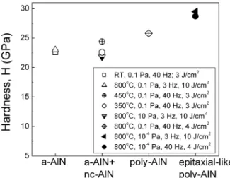
The hardness values of the AlN films as a function of the film structure are shown in Figure7.
The data demonstrate well the sensitivity of the AlN film structure to the PLD conditions. As can be seen, the PLD AlN films with the amorphous structure possessed the lowest hardness values.
The reason is that the amorphous material is characterized by a short-range order with a distribution in bond lengths that generally results in lower stiffness, as compared to the corresponding crystalline phase [55]. The higher the stiffness of the atomic bondings, the higher the material’s hardness is.
This explains the observed increased hardness of the PLD AlN films when the degree of crystallinity increased for example by enhancing the substrate temperature from 350 to 800◦C or increasing the LPF from 3 to 40 Hz, respectively.
Coatings 2019, 9, x FOR PEER REVIEW 10 of 17
Figure 7. Variation of the hardness values with the film structure obtained at different PLD conditions, given in the inset.
3.3. FTIR Reflectance Spectra Analysis
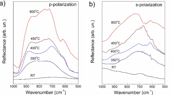
FTIR reflectance spectra are given in Figure 8 for the case of p-polarized (Figure 8a) and s-polarized (Figure 8b) incident beams recorded at a radiation angle of 70°. The results in Figure 8 correspond to AlN films deposited with a laser fluence of 3 J/cm2 and different temperatures and LPF of 40 Hz. For higher temperatures, the spectra exhibited a complex and broad band within the 950‒500 cm‒1 region.
The complexity of the spectral envelope can be assigned to the nanocrystallites’ disorientation. The Berreman effect was registered in p-polarization, which allows for identification of the longitudinal (LO) phonon vibrational modes [59]. This gives the possibility to characterize thin films’ microstructure directly from IR spectroscopy. A comparison of the spectra taken in both s- and p-polarization points to a clear difference in the high frequency end of the band (Figure 8).
Figure 8. FTIR reflectance spectra of PLD AlN films, investigated in a linearly p-polarized (a) and s-polarized (b) incident beam.
The 950‒500 cm‒1 region is characteristic for the Reststrahlen band of the h-AlN crystal with component lines peaking around 611, 670, 890, and 912 cm–1, arising from A1(TO), E1(TO), A1(LO), and E1(LO) IR active phonon vibrational modes, respectively [60–63]. For samples prepared at low substrate temperatures (RT and 350 °C), the deconvolution of the measured Reststrahlen band in p-polarized
Figure 7.Variation of the hardness values with the film structure obtained at different PLD conditions, given in the inset.
One can observe in Figure7that the appearance of nanocrystallites in the amorphous matrix increased the AlN film’s hardness. The size and amount of crystallite grains are determinative in the hardness level of coatings [56–58]. However, when two phases coexist in films, the hardness values can be greatly influenced by the thickness of the amorphous matrix separating the nanocrystals. Moreover, when the crystalline particles are forming in the gas space, it is easier to involve cavities (voids) from their environment, which can greatly reduce the hardness of the layer.
The highest hardness values were registered for the PLD films with epitaxial-like growth of AlN on the Si(100) substrates, i.e., when the PLD process proceeded in vacuum at the highest temperature (800◦C) (see Figure7). In this case, the largest size of nanocrystallites (10–20 nm),
Coatings2019,9, 195 10 of 16
growing in a columnar grain structure with preferred grain orientations and in a negligible amount of amorphous matter, was observed (Figures5b and6). Such an ordered structure is characterized by a strongly-reduced amount of defects in grain boundaries and, consequently, a higherHvalue, as was observed.
3.3. FTIR Reflectance Spectra Analysis
FTIR reflectance spectra are given in Figure8for the case ofp-polarized (Figure8a) ands-polarized (Figure8b) incident beams recorded at a radiation angle of 70◦. The results in Figure8correspond to AlN films deposited with a laser fluence of 3 J/cm2and different temperatures and LPF of 40 Hz.
For higher temperatures, the spectra exhibited a complex and broad band within the 950–500 cm−1 region. The complexity of the spectral envelope can be assigned to the nanocrystallites’ disorientation.
The Berreman effect was registered inp-polarization, which allows for identification of the longitudinal (LO) phonon vibrational modes [59]. This gives the possibility to characterize thin films’ microstructure directly from IR spectroscopy. A comparison of the spectra taken in boths- andp-polarization points to a clear difference in the high frequency end of the band (Figure8).
Coatings 2019, 9, x FOR PEER REVIEW 10 of 17
Figure 7. Variation of the hardness values with the film structure obtained at different PLD conditions, given in the inset.
3.3. FTIR Reflectance Spectra Analysis
FTIR reflectance spectra are given in Figure 8 for the case of p-polarized (Figure 8a) and s-polarized (Figure 8b) incident beams recorded at a radiation angle of 70°. The results in Figure 8 correspond to AlN films deposited with a laser fluence of 3 J/cm2 and different temperatures and LPF of 40 Hz. For higher temperatures, the spectra exhibited a complex and broad band within the 950‒500 cm‒1 region.
The complexity of the spectral envelope can be assigned to the nanocrystallites’ disorientation. The Berreman effect was registered in p-polarization, which allows for identification of the longitudinal (LO) phonon vibrational modes [59]. This gives the possibility to characterize thin films’ microstructure directly from IR spectroscopy. A comparison of the spectra taken in both s- and p-polarization points to a clear difference in the high frequency end of the band (Figure 8).
Figure 8. FTIR reflectance spectra of PLD AlN films, investigated in a linearly p-polarized (a) and s-polarized (b) incident beam.
The 950‒500 cm‒1 region is characteristic for the Reststrahlen band of the h-AlN crystal with component lines peaking around 611, 670, 890, and 912 cm–1, arising from A1(TO), E1(TO), A1(LO), and E1(LO) IR active phonon vibrational modes, respectively [60–63]. For samples prepared at low substrate temperatures (RT and 350 °C), the deconvolution of the measured Reststrahlen band in p-polarized
Figure 8. FTIR reflectance spectra of PLD AlN films, investigated in a linearlyp-polarized (a) and s-polarized (b) incident beam.
The 950–500 cm−1region is characteristic for the Reststrahlen band of theh-AlN crystal with component lines peaking around 611, 670, 890, and 912 cm−1, arising from A1(TO), E1(TO), A1(LO), and E1(LO) IR active phonon vibrational modes, respectively [60–63]. For samples prepared at low substrate temperatures (RT and 350◦C), the deconvolution of the measured Reststrahlen band inp-polarized radiation was not possible. For higher substrate temperatures, the position of peaks was determined by the Levenberg–Marquardt deconvolution method with a fitting mean square error of 10−3. The peaks and their assignments are collected in Table1. When decreasing the substrate temperature, a major decrease of frequencies was observed for the E1(TO) and A1(LO) phonon-polariton modes. At a large angle ofp-polarized incidence radiation such as 70◦, the A1(LO) mode, which is polarized parallel to the nanocrystallitec-axis, will be the most sensitive to the orientation of the crystal phase (Figure8a).
Any deviation ofc-axis from the surface normal leads to a structure disorientation that is equivalent to a dumping of the phonon-polariton resonance vibration [64]. The enhanced structure disordering at lower temperatures also influences the E1(TO) mode, which is polarized parallel to thea-axis, i.e., is parallel to the substrate surface in a goodc-axis-oriented layer. Consequently, the resonance frequency decrease was more evident in the spectra measured ins-polarization (see Figure8b). Besides, this mode is two-fold degenerated, i.e., it cumulates vibrations of two sets of atoms with the same
Coatings2019,9, 195 11 of 16
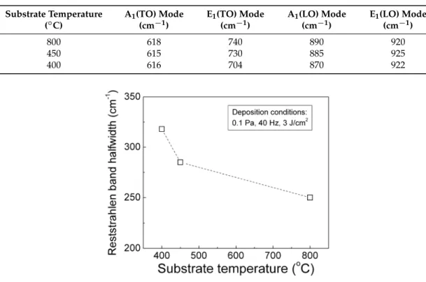
frequency [65]. Thus, an increasing disorder with the temperature decrease will cause the peak’s widening (as observed for all components), which leads to an increase of the entire Reststrahlen band half width. This is illustrated in Figure9for the AlN films deposited at 0.1 Pa N2pressure and LPF of 40 Hz. The incident laser fluence was kept within the range of 3–4 J/cm2.
It should be mentioned that the features around 620–610 cm−1in both sets of spectra in Figure8 could hardly be assigned to the phonon mode A1(TO) ofh-AlN only. Indeed, the vibrational modes of Si substrate [66] and those of possible AlOxphases [67] were also present in the above-mentioned region. Possible AlOxbonds could be formed either during film preparation or storage of the samples under atmospheric conditions. In our opinion, the latter assumption is more likely to occur.
Table 1. Peak position of the phonon-polariton modes in the Reststrahlen band, registered with p-polarized radiation in the AlN films (Figure8a). TO, transverse.
Substrate Temperature (◦C)
A1(TO) Mode (cm−1)
E1(TO) Mode (cm−1)
A1(LO) Mode (cm−1)
E1(LO) Mode (cm−1)
800 618 740 890 920
450 615 730 885 925
400 616 704 870 922
Coatings 2019, 9, x FOR PEER REVIEW 11 of 17
radiation was not possible. For higher substrate temperatures, the position of peaks was determined by the Levenberg–Marquardt deconvolution method with a fitting mean square error of 10–3. The peaks and their assignments are collected in Table 1. When decreasing the substrate temperature, a major decrease of frequencies was observed for the E1(TO) and A1(LO) phonon-polariton modes. At a large angle of p-polarized incidence radiation such as 70°, the A1(LO) mode, which is polarized parallel to the nanocrystallite c-axis, will be the most sensitive to the orientation of the crystal phase (Figure 8a). Any deviation of c-axis from the surface normal leads to a structure disorientation that is equivalent to a dumping of the phonon-polariton resonance vibration [64]. The enhanced structure disordering at lower temperatures also influences the E1(TO) mode, which is polarized parallel to the a-axis, i.e., is parallel to the substrate surface in a good c-axis-oriented layer. Consequently, the resonance frequency decrease was more evident in the spectra measured in s-polarization (see Figure 8b). Besides, this mode is two-fold degenerated, i.e., it cumulates vibrations of two sets of atoms with the same frequency [65].
Thus, an increasing disorder with the temperature decrease will cause the peak’s widening (as observed for all components), which leads to an increase of the entire Reststrahlen band half width. This is illustrated in Figure 9 for the AlN films deposited at 0.1 Pa N2 pressure and LPF of 40 Hz. The incident laser fluence was kept within the range of 3‒4 J/cm2.
It should be mentioned that the features around 620–610 cm–1 in both sets of spectra in Figure 8 could hardly be assigned to the phonon mode A1(TO) of h-AlN only. Indeed, the vibrational modes of Si substrate [66] and those of possible AlOx phases [67] were also present in the above-mentioned region.
Possible AlOx bonds could be formed either during film preparation or storage of the samples under atmospheric conditions. In our opinion, the latter assumption is more likely to occur.
Table 1. Peak position of the phonon-polariton modes in the Reststrahlen band, registered with p-polarized radiation in the AlN films (Figure 8a). TO, transverse.
Substrate Temperature (°C)
A1(TO) Mode (cm‒1)
E1(TO) Mode (cm‒1)
A1(LO) Mode (cm‒1)
E1(LO) Mode (cm‒1)
800 618 740 890 920 450 615 730 885 925 400 616 704 870 922
Figure 9. Reststrahlen band half width in p-polarized radiation (Figure 6a) as a function of substrate temperature during AlN film deposition at N2 pressure of 0.1 Pa, LPF of 40 Hz, and laser fluence of 3‒4 J/cm2.
From the presented results, one can conclude that despite the poor crystalline phase, revealed by TEM, the FTIR spectra of AlN thin films deposited at temperatures higher than 350 °C clearly exhibited the characteristic Reststrahlen band of the AlN crystal with a hexagonal lattice. This band was
Figure 9.Reststrahlen band half width inp-polarized radiation (Figure6a) as a function of substrate temperature during AlN film deposition at N2pressure of 0.1 Pa, LPF of 40 Hz, and laser fluence of 3–4 J/cm2.
From the presented results, one can conclude that despite the poor crystalline phase, revealed by TEM, the FTIR spectra of AlN thin films deposited at temperatures higher than 350◦C clearly exhibited the characteristic Reststrahlen band of the AlN crystal with a hexagonal lattice. This band was originating from theh-AlN nanocrystallites, the size and ordering of which were increasing with the substrate temperature. For the AlN films synthesized at a substrate temperature of 350◦C, the spectra did not preserve the shape of a Reststrahlen band, and therefore, if nanocrystals were formed, their contribution could be negligible. At RT, a completely amorphous layer was grown. According to the SE results, the optical thickness of this layer was relatively small with respect to the wavelengths of the measured spectral region (~λ/20), and the recorded FTIR spectrum was flat. In such a thin amorphous film, neither a Reststrahlen band, nor the multiple interference effect could be observed in the FTIR spectra [68].
3.4. Spectroscopic Ellipsometry
The ellipsometric results revealed a clear dependence on technological conditions, in good agreement with TEM and FTIR investigations. We note that each AlN film yielded a certain
Coatings2019,9, 195 12 of 16
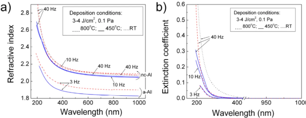
thickness, which was within the 400–1000-nm range (corresponding to an estimated deposition rate of ~2.8×10⁻²–7×10⁻²nm/pulse), depending on the PLD technological protocol. For illustration purposes, in Figure10, the optical constantsnandkare shown for AlN films deposited in ambient nitrogen at a pressure of 0.1 Pa and laser fluence of 3–4 J/cm2, by varying the substrate temperature and LPF. These values are characteristic for the corresponding AlN structures and correlated well with TEM observations. The refractive index values either coincided or were superior to those of amorphous AlN and remained inferior to those of high-quality polycrystallineh-AlN films. This suggests the coexistence of crystalline and amorphous AlN phases. Independently of the substrate’s deposition temperature, films deposited at LPF of 3 Hz (Figure10) possessednvalues characteristic to an amorphous AlN structure. In accordance with the TEM results, larger LPF yielded nanostructured films with better ordering at LPF of 10 Hz, which reflects slightly higher index values. The exception is the AlN film deposited at RT (data represented by black dots in Figure10), which was completely amorphous, as revealed by TEM, but itsnvalues were close to those ofnc-AlN. Additional compositional study of this sample by energy dispersive spectroscopy (EDS), performed in a scanning electron microscopy (SEM) system, has disclosed an over-stoichiometric AlN with an average Al/N ratio of 1.14. One can notice from the SEM-EDS results in Table2that at elevated temperatures, the films’ composition was close to the stoichiometric AlN. When deposited at RT, AlN films contained an excess amount of Al atoms, which could contribute to the observed higher index values.
Coatings 2019, 9, x FOR PEER REVIEW 12 of 17
originating from the h-AlN nanocrystallites, the size and ordering of which were increasing with the substrate temperature. For the AlN films synthesized at a substrate temperature of 350 °C, the spectra did not preserve the shape of a Reststrahlen band, and therefore, if nanocrystals were formed, their contribution could be negligible. At RT, a completely amorphous layer was grown. According to the SE results, the optical thickness of this layer was relatively small with respect to the wavelengths of the measured spectral region (~λ/20), and the recorded FTIR spectrum was flat. In such a thin amorphous film, neither a Reststrahlen band, nor the multiple interference effect could be observed in the FTIR spectra [68].
3.4. Spectroscopic Ellipsometry
The ellipsometric results revealed a clear dependence on technological conditions, in good agreement with TEM and FTIR investigations. We note that each AlN film yielded a certain thickness, which was within the 400‒1000-nm range (corresponding to an estimated deposition rate of
~2.8 × 10⁻²–7 × 10⁻² nm/pulse), depending on the PLD technological protocol. For illustration purposes, in Figure 10, the optical constants n and k are shown for AlN films deposited in ambient nitrogen at a pressure of 0.1 Pa and laser fluence of 3‒4 J/cm2, by varying the substrate temperature and LPF. These values are characteristic for the corresponding AlN structures and correlated well with TEM observations. The refractive index values either coincided or were superior to those of amorphous AlN and remained inferior to those of high-quality polycrystalline h-AlN films. This suggests the coexistence of crystalline and amorphous AlN phases. Independently of the substrate’s deposition temperature, films deposited at LPF of 3 Hz (Figure 10) possessed n values characteristic to an amorphous AlN structure. In accordance with the TEM results, larger LPF yielded nanostructured films with better ordering at LPF of 10 Hz, which reflects slightly higher index values. The exception is the AlN film deposited at RT (data represented by black dots in Figure 10), which was completely amorphous, as revealed by TEM, but its n values were close to those of nc-AlN. Additional compositional study of this sample by energy dispersive spectroscopy (EDS), performed in a scanning electron microscopy (SEM) system, has disclosed an over-stoichiometric AlN with an average Al/N ratio of 1.14. One can notice from the SEM-EDS results in Table 2 that at elevated temperatures, the films’ composition was close to the stoichiometric AlN. When deposited at RT, AlN films contained an excess amount of Al atoms, which could contribute to the observed higher index values.
Figure 10. Dispersion curves of the refractive index (a) and extinction coefficient (b) of the studied AlN films deposited in the conditions presented in the insets.
Figure 10.Dispersion curves of the refractive index (a) and extinction coefficient (b) of the studied AlN films deposited in the conditions presented in the insets.
Table 2.SEM-EDS data for AlN films deposited at different substrate temperatures in ambient N2at a pressure of 0.1 Pa, incident laser fluence of 3 J/cm2, and LPF of 40 Hz.
Substrate Temperature (◦C) Al/N Atomic Ratio
800 0.98
450 0.98
350 0.97
RT 1.14
PLD AlN films were transparent in the 400–1000-nm spectral region, as thekvalues, dependent on substrate temperature and LPF (Figure10b), approached zero. Below 400 nm, because of reaching the absorption edge, the extinction coefficient increased, and its value varied with the deposition conditions. A large shift of the absorption edge to higher wavelengths was observed for the RT deposited AlN film, suggesting a strong reduction of the optical bandgap in comparison to those deposited at elevated temperatures.
Coatings2019,9, 195 13 of 16
4. Conclusions
Aluminum nitride (AlN) films with different structural features were synthesized onto Si(100) substrates by pulsed laser deposition in vacuum and ambient nitrogen, at various pressures, substrate temperatures, laser incident fluences, and laser pulse frequencies. From the results of nanoindentation tests, transmission electron microscopy, X-ray diffraction, atomic force microscopy, Fourier transform infrared spectroscopy, and spectroscopic ellipsometry, the correlation between the mechanical properties, film structure, and optical parameters, dependent on deposition conditions, was studied.
The growth process and resulting film microstructures yielded variation in the film hardness within 22–30 GPa. Elevated substrate temperatures facilitated the crystallization process and, thus, a less defective structure for which increased nanohardness values were reached. Enhanced hardness values, in the range of 22–27 GPa, were observed for AlN films with a structure that consisted of nanocrystallite grains of 5–50 nm embedded in an amorphous matrix, strongly dependent on the deposition conditions. These values were superior to those obtained by other deposition techniques or reported for crystalline AlN. The refractive index value, superior to that of amorphous AlN, supported the existence of crystallites inside the film volume. In the case of PLD AlN films deposited at temperatures higher than 350◦C, the FTIR results evidenced vibrational bands within the characteristics Reststrahlen band of 950–500 cm−1, which were assigned to hexagonal AlN crystallites. For lower temperatures, the Reststrahlen band gradually vanished, and the PLD film at room temperature exhibited an FTIR spectrum characteristic of a completely-amorphous AlN material.
The mechanical and optical properties of the synthesized AlN films conformed to the applied PLD technological parameters.
Author Contributions:Conceptualization, A.S. and L.D.; methodology, P.T., Z.F., and L.D.; validation, L.K., A.S., K.A., P.P., and L.D.; formal analysis, K.A., and P.T.; investigation, L.K., V.C., K.A., Z.F., and L.D.; resources, I.N.M.;
writing, original draft preparation, L.K., A.S., K.A., and L.D.; writing, review and editing, A.S., P.P., I.N.M., and L.D.; visualization, L.D.; supervision, A.S.; project administration, A.S. and L.D.
Funding:The Bulgarian co-authors thank the European Regional Development Fund, the Ministry of Economy of Bulgaria, Operational Programme “Development of the Competitiveness of the Bulgarian economy” 2007–2013, Contract No. BG161PO003-1.2.04-0027-C0001. The Romanian co-authors acknowledge the support of the Core Programme, Contract 16N/2019. Liviu Duta thanks the support from the grant of the Ministry of Research and Innovation, CNCS-UEFISCDI, Project Number PN-III-P1-1.1-PD-2016-1568 (PD 6/2018), within PNCDI III. Peter Petrik is grateful for the support from OTKA Grant No. K115852.
Acknowledgments:All authors acknowledge with thanks the support of this work by the Bulgarian, Hungarian, and Romanian Academies of Sciences under the 2014–2017 Collaboration Agreements.
Conflicts of Interest:The authors declare no conflict of interest.
References
1. Chrisey, D.B.; Hubler, G.K.Pulsed Laser Deposition of Thin Films; John Wiley & Sons: Hoboken, NJ, USA, 1994.
2. Eason, R. Pulsed Laser Deposition of Thin Films—Applications-Led Growth of Functional Materials;
Wiley-Interscience: Hoboken, NJ, USA, 2007.
3. Koh, A.T.T.; Foong, Y.M.; Chua, D.H.C. Cooling rate and energy dependence of pulsed laser fabricated graphene on nickel at reduced temperature.Appl. Phys. Lett.2010,97, 114102. [CrossRef]
4. Yang, Z.; Hao, J. Progress in pulsed laser deposited two-dimensional layered materials for device applications.
J. Mater. Chem. C2016,4, 8859–8878. [CrossRef]
5. Rodriguez, R.J.; Garcia, J.A.; Medrano, A.; Rico, M.; Sanchez, R.; Martinez, R.; Labrugère, C.; Lahaye, M.;
Guette, A. Tribological behaviour of hard coatings deposited by arc-evaporation PVD.Vacuum2002,67, 559–566. [CrossRef]
6. Huang, Z.P.; Sun, Y.; Bell, T. Friction behaviour of TiN, CrN, (TiAl)N coatings. Wear1994, 173, 13–20.
[CrossRef]
7. Jianxin, D.; Aihua, L. Dry sliding wear behavior of PVD TiN, Ti55Al45N, and Ti35Al65N coatings at temperatures up to 600◦C.Int. J. Refract. Met. Hard Mater.2013,41, 241–249. [CrossRef]