The effect of substrate bias on the piezoelectric
properties of pulse DC magnetron sputtered AlN thin films
Nguyen Quoc Kha´nh1,* , Ja´nos Rado´1, Zsolt Endre Horva´th1, Saeedeh Soleimani1, Binderiya Oyunbolor1, and Ja´nos Volk1
1Centre for Energy Research, Institute of Technical Physics and Materials Science, Konkoly-Thege M. út 29-33, H-1121 Budapest, Hungary
Received:27 July 2020 Accepted:1 November 2020 Published online:
13 November 2020
Ó
The Author(s) 2020ABSTRACT
Substrate bias was applied for AlN deposition on rolled Ni sheet during pulse DC reactive sputtering to overcome the difficulty caused by thermal expansion mismatch between Ni substrate and AlN upon substrate heating. It was shown by Piezoresponse Force Microscopy (PFM) that the quality of the deposited AlN layer depends strongly on the negative substrate bias, i.e., the energy transferred via the bombardment of the accelerated positive ions on the sample. As the negative substrate bias becomes larger, the so formed layer shows higher piezoresponse, and better homogeneity. A Z-cut LiNbO3single crystal was used as a reference to correct the PFM signals. The highest average d33piezoelectric coefficient value, achieved at-100 V substrate bias, is 3.4 pm/V indicating the feasibility of AlN deposition on rolled Ni substrate for vibration energy har- vesting applications.
1 Introduction
Tremendous number of sensors to be applied nowa- days over the world necessitates the use of sustain- able, maintenance-free, and self-powered sensor system [1]. Piezoelectric materials are promising for such purpose, being a good transducer to convert directly the stimulus into electric signal in the case of sensing, or into electrical energy as vibrational energy harvesters for sensor operation.
Aluminum nitride (AlN) thin film has been widely studied for piezoelectric energy harvester
application, among others, due to its excellent prop- erties, like piezoelectricity even at high temperature, extreme hardness, good thermal and chemical sta- bilities, and not least, environment friendly lead-free material. [2]. AlN films can be grown by various methods including Chemical Vapor Deposition (CVD) [3], MetalOrganic Chemical Vapor Deposition (MOCVD) [4], Molecular Beam Epitaxy (MBE) [5], Pulsed Laser Deposition (PLD) [6], and Atomic Layer Deposition (ALD) [7]. However, these methods are expensive, and high processing temperatures are required. Direct Current (DC) and Radio Frequency Address correspondence toE-mail: khanh@mfa.kfki.hu
https://doi.org/10.1007/s10854-020-04810-9
(RF) reactive ion sputtering, being low temperature and low-cost processes with excellent reproducibility and high output, therefore, are the most frequently applied techniques to produce AlN thin layer [8–10].
Silicon wafer (with or without top oxide) is the most commonly used substrate for AlN deposition.
Depending on requirements of the device to be fab- ricated different metals are deposited as buried electrode prior to AlN growth [11–14]. Sometimes sapphire or glass substrate have been also used [15,16]. Common character of these substrates is their smooth surface, which is indispensable for certain applications, like Surface Acoustic Wave Sensor (SAWS) [12,17], and Film Bulk Acoustic Resonators (FBAR) [9]. It is a consensus among researchers that the character of the substrate surface has a role as important as the deposition conditions on the prop- erties of the AlN crystal grown on it, that is substrate crystal lattice and surface morphology all affect the (002) preferential growth of AlN film [11,13,14].
In a few MEMS applications metal substrate is a viable alternative of Si where the high fracture toughness, low substrate and micromachining costs are concerned. For example, unimorph piezoelectric energy harvesters, which convert mechanical energy into electricity, require a relatively large area, high mechanically robustness therefore laser cut metal film, such as stainless steel [18] or Ni is a reasonable choice. Generally, a substrate heating of c.a. 500°C is applied during the growth of AlN to improve its crystal quality via enhancing the surface diffusion [9,16, 19,20]. However, in the case of Ni sheet, the substrate heating is not applicable due to the high difference of thermal expansion coefficient between Ni substrate (13910-6K-1) [21] and AlN (4.2910-6 K-1) [22]. So one can expect that as the sample cools down from high temperature after deposition, the adhesion between AlN layer and Ni substrate can degrade significantly, even AlN layer can detach from Ni substrate, which makes the application of such structure for vibration energy harvester impos- sible. For this reason, we have applied the new approach, namely the negative bias on Ni substrate during deposition of AlN layer at room temperature.
The substrate bias can affect the quality of deposited layer via the impact of the energetic ions on the sample surface [16,23–25]. By increasing the energy supplied to the film the surface diffusion can be enhanced, leading to an increase in the mean distance which the adatoms can travel, reaching the lowest
energy sites [26], thus results in an improved crystal growth. In return, one may expect the resputtering at the substrate, which may decrease the rate of the AlN layer deposition.
Though the piezoelectric coefficient can be mea- sured by macroscopic techniques, like Berlincourt Piezometer [27], series capacitance [28], interferome- ter [29], but characterization in nanoscale (elec- tromechanical displacement variation, polarity) using Piezoresponse Force Microscopy (PFM) [30,31] helps to understand better the influence of deposition parameters on piezoelectric properties of the depos- ited AlN layer, and so to optimize the parameters of the deposition process. In PFM measurement, contact resonance could be applied to enhance the sensitivity.
However, delicate techniques are needed to handle the problem of contact resonance shift caused by the surface morphology, like Dual-Frequency Resonance- Tracking (DFRT) PFM [32], or Band-Excitation (BE) PFM [33]. Furthermore, model calculations are nee- ded to make correction on the results [34,35]. In lack of the listed techniques, off-resonant measurement is a reasonable choice; however, one should take into account that the signal-to-noise ratio is deteriorated, and the electrostatic effect is still to be considered in this case. The latter one could be essential in the PFM signal, hence make such measurement unreliable.
Therefore, elimination of the electrostatic contribu- tion is vital point in PFM measurement.
In this report we used PFM and X-Ray Diffrac- tometry (XRD) techniques to investigate the effect of substrate bias on the quality of AlN layer first time deposited at RT on 80lm thick rolled Ni sheet which is ready to use as the active element of the flexible energy harvester. A Z-cut LiNbO3 crystal (z-LN) having well-known piezocoefficients has been used as a reference for the correction of PFM results.
2 Experimental
2.1 Sample preparationRolled Ni sheets with thickness of 80 lm have been ultrasonically cleaned stepwise in acetone, ethanol, deionized water for 5 min, and purged in nitrogen.
Then the sample was loaded into the chamber of the pulse DC magnetron sputtering system (VAKSIS- MiDAS). The base pressure was in the range of 3–69 10-8Torr. The substrate was further cleaned by 30 W
Ar plasma for 10 min. Then AlN films were depos- ited onto Ni substrates by reactive sputtering with constant parameters except for deposition time and substrate bias voltage. The sputtering cathode was thick pure Al target (99.999%) and was continuously water cooled. The gases used are high-purity argon (99.999%) as the working gas and nitrogen (99.999%) as reactive gas. During deposition total pressure was 5 mTorr, and no intentional heating was applied, the estimated substrate temperature due to plasma heating is around 100 °C. The detailed deposition conditions are listed in Table1.
2.2 Characterization
Atomic Force Microscopy (AIST NT smart-SPM1000) was used to study the morphology of the films in semi-contact mode, as well as piezoelectric properties of AlN layer in top-PFM mode, i.e., the probe movement between scan raster points is performed in semi-contact mode, while PFM measurement is car- ried out in the raster points using contact mode technique. This hybrid operation mode enables the use of stiff cantilever for PFM scan. For studying the electrostatic effect, at first three kinds of tips with 0.2, 3, 42 N/m spring constant were compared on thick SiO2 thermally grown on p-silicon sample with thickness of 1.3lm like that of AlN films, where the bottom electrode was 100 nm Al sintered in forming gas for 30 min to achieve ohmic contact with p-Si.
Later on, for the actual PFM tests a conductive probe with spring constant of 42 N/m was used (PPP- NCHPt, Nanosensors). The pressing force to the tip was kept at 120 nN for contact mode. The amplitude and frequency of the exciting Vacwere in the range of 0–9 V and 51 kHz, respectively. However, Vacup to 4 V was applied in most case to avoid the fast
degradation of the tip according to our PFM experi- ence. The measured data have been evaluated by Gwyddion software package [36]. For comparison, the samples were also measured by Berlincourt piezometer (Piezotest PM300) using 10.4 N static force (preload), and 0.25 N dynamic force at 110 Hz frequency.
To investigate the structure of the obtained films, a Bruker AXS D8 Discover diffractometer was used in Bragg-Brentano geometry (h–2h geometry), at room temperature; with Cu Ka radiation. The XRD diffractograms were obtained at scanned angle of 2h varying from 30 to 70°. The film thicknesses were measured by Scanning Electron Microscope (SEM) at the cross-section of the cleaved sample.
3 Results and discussion
3.1 Surface morphology of the films
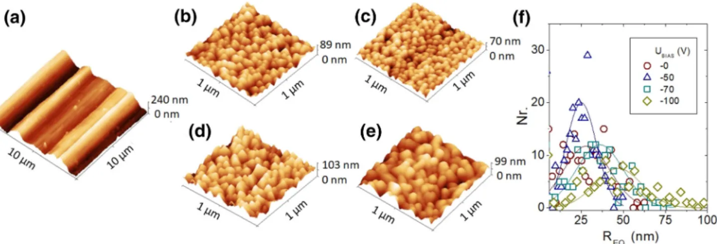
Ni substrate, being rolled sheet, has a wavy feature with height fluctuates within few hundred nanome- ters (Fig. 1a). It is clear that the surface roughness on large area is dominated by the substrate. Therefore, the roughness of the AlN layer is only correctly measured on the area with dimension of c.a. 1lm, where the substrate is relatively flat. For this reason, both AFM, and PFM have been carried out on sample area of 191lm2.
Figure1b–e shows the AFM height images of the AlN layers deposited with different bias voltages, from which the grain size and surface roughness (in RMS) were determined. The in-plane grain size was characterized by equivalent disk radius using the watershed algorithm in Gwyddion. Because of small scanned area, the size distributions are somewhat scattered. The mean grain size increases slightly with increasing bias voltage from ca. 28 nm for unbiased sample to 46 nm for -100 V bias (Fig. 1f). The sur- face roughness, however, remains around 14 nm for all applied bias voltage. Deposition rate was deter- mined using the thickness measured by SEM on the cross-section of the samples, and deposition time.
The deposition rate decreases from 13.4 to 10.4 nm/
min as the bias voltage increases from 0 to - 70 V, then increases to 14.6 nm/min. for-100 V substrate bias. The rates are acceptable in all cases indicating that the resputtering is tolerable in the range of applied substrate bias. Deposition rate also seems to Table 1 Sputtering conditions for the deposition of AlN films
Target Pure aluminum (3 inch, 99.999%)
Target-substrate distance 13 cm
Base pressure 3.0910-8Torr Ar/N2gas flow rates 80/20 sccm Working gas pressure 5 mTorr
Sputtering power 370 W
Deposition time 90–120 min
Bias substrate 0,-50,-70 and-100 V Substrate temperature *100°C (plasma heating)
change oppositely compared to the surface roughness for different substrate bias; the higher the deposition rate the smoother the surface is.
3.2 The effect of the cantilever stiffness
Together with the electromechanical displacement (DEM) the utmost non-piezoelectric contribution to the displacement (DPR) measured by PFM is caused by the electrostatic force between sample and tip, as well as sample and cantilever. Practically the elec- trostatic part is handled as the first harmonic of the cantilever oscillation due to alternating excitation voltage [37,38]
Dx;ES¼k1dC
dzðVdcþVCPDÞVacsinðxtÞ
where Dx;ES is the electrostatic displacement, k, C, Vdc, VCPD, and VacsinðxtÞ are the spring constant, contact capacitance, optional DC voltage, contact potential difference, and AC voltage, respectively.
From the equation above one can see that the effect of the electrostatic force can be eliminated by appli- cation of proper Vdc, or by the use of a stiff cantilever.
We used a 1.3lm thick oxide thermally grown on p-silicon, i.e., non-piezoelectric sample to show the benefit of stiff cantilever. Figure2 shows the dis- placement measured using cantilevers with different spring constants as a function of Vac. Since Vdccannot be set in our scanning probe system, only Vac was applied. For each Vac bias 100 acquisitions with 100 ms acquisition time were recorded at the same position of the sample surface. Because of the smooth surface and excellent homogeneity of the SiO2 thin
films no area averaging was needed, in contrast to the polycrystalline AlN films.
As one can see in Fig. 2, the effect of electrostatic force decreases as the stiffness of the probe cantilever increases. For the stiffest cantilever of 42 N/m, the electrostatic contribution, which could cause a sig- nificant error in the piezoelectric properties deter- mined from the measured data, is practically eliminated.
3.3 Piezoelectric response
Figure3shows the amplitude map measured by PFM at Vac= 4 V for AlN films sputtered at different bias voltages (Vbias). The sample sputtered under zero bias shows very weak piezoresponse indicating a Fig. 1 AFM height image of rolled Ni substrate (a), small area scan on the AlN layer deposited with Vbiasof 0V (b),-50 V (c),-70 V (d),-100 V (e) and the corresponding grain size distributions (f)
Fig. 2 PFM displacement responses due to electrostatic force on non-piezoelectric SiO2blank sample. The electrostatic coefficients also shown in the legend
poor crystal quality, or crystal growth in inferior direction. There are few small areas showing elec- tromechanical (EM) displacement around 1-2 pm over background for Vac= 4 V. The major part of the image equal to the background level determined by fitting the piezoresponses at different Vac, i.e., the intersection of fitting line with the displacement (y) axis. Such dead zones (DZ) are marked by dark cyan in Fig. 3. The ratio of dead zones decreases as bias voltage gets larger. Practically no DZ is found on sample biased with-100 V. Also, the EM displace- ment outside DZs shows higher value as larger sub- strate bias was applied. The attenuation of dead zone and the increasing in displacement both reveal the benefit of applying substrate bias.
The distribution of PFM response gives informa- tion on the homogeneity of the layer. The narrower the distribution, the more homogeneous the layer is.
In the present case the phase output of the lock-in amplifier was manually shifted to 0 to ease the comparison (Fig.4b). The y-axis represents the probability density function for which the integration over the entire displacement space equals to 1. The amplitude distribution of unbiased sample is at the background level, while its phase distribution is extremely wide. As bias voltage increases, the layer becomes more and more homogeneous, i.e., the phase distribution is narrower and higher. Though
the displacement distribution peak of unbiased sample is narrow, and high, it is due to the fact that it contains mainly the background. Interestingly, increasing substrate bias from 50 to 70 V has almost no effect on the amplitude and phase distribution.
For the best sample (Vbias = -100 V) the mean dis- placement is c.a. 6.5 pm at VAC= 4 V, and the FWHM of phase distribution is about 22°.
For the determination of the effective piezoelectric coefficient, one should measure the EM displacement at different exciting AC voltage to eliminate the background. Figure 5 presents the measured dis- placement as a function of Vac. Each point is the average of a 1289128 point scan over 191lm2area of the samples. The slope of the displacement-voltage fitting line gives the effective EM coefficient. The highest effective coefficient of 1.59 pm/V achieved at Vbias=-100 V bias is rather small compared to the value of 5.6 pm/V for bulk AlN.[39]
3.4 Correction of the PFM data
The measured effective coefficients are well below the intrinsic value. One reason of low measured value can be the clamp effect, that is the thin layer to be measured is not under free boundary condition, but it is clamped to the substrate. Therefore, the measured effective piezoelectric coefficient d33eff of thin layer
Fig. 3 Piezoresponse amplitude image of AlN layers deposited with Vbias=-0 V (a),-50 V (b),-70 V (c),- 100 V (d). PFM carried out with Vac = 4 V. Area with background equivalent displacement marked by dark cyan
can be related to the unclamped oned33 by the fol- lowing relationship [40]:
d33;unclamp¼d33;eff SE11þSE12
SE11þSE12þSE13
Using SE11 ¼3, SE12 ¼ 0:9, SE13 ¼ 0:6 TPa-1 [41]
the clamp effect correction factor is Cclamp= 1.4.
The second origin of the underestimated piezoco- efficient is the tip-shape effect, i.e., the electrostatic field below the sharp tip is not homogenous and depends on the radius of the tip, in contrast to the macroscopic piezometer technique which can be described by a parallel plate capacitor model. To correct this effect, a second correction was performed using a Z-cut LiNbO3single crystal (z-LN) reference with a thickness of c.a. 300lm. The displacement of z-LN surface as a function of exciting Vacis presented
in Fig. 6, from which the effective coefficient obtained by linear fitting is 4.1 pm/V which is smaller com- pared to the intrinsic one of z-LN (6.2 pm/V) [42]. We note that the clamp effect mentioned above is not the case here, because the crystal is much thicker than the thickness limit of the layer, within which the clamp effect is valid [29]. Taking into account the clamp effect and the calibration on z-LN a consolidated correction factor of Ccons = 6.2/4.1 9 Cclamp = 2.12 was calculated.
d33¼Cconsd33;eff
Using Ccons correction factor, the best average value obtained by substrate bias of - 100 V is 3.4 pm/V. The map of the local d33that is the corrected d33distribution in nanoscale of the AlN films can be obtained using the linear fit of corresponding points of the displacement data sets measured at different
0 2 4 6 8 10
0.0 0.1 0.2 0.3 0.4 0.5 0.6
PFM 4V, 120nN, 51 kHz
(a)
ρ (pm-1 )
Displacement (pm)
V
bias (-V)
0
50
70
100
-100 -50 0 50 100 0.00 0.02 0.04 0.06
(b)
PFM 4V, 120nN, 51 kHz ρ (deg-1 ) Phase (deg) Vbias (-V) 050
70
100
Fig. 4 Amplitude (a) and phase (b) distribution of samples deposited at various substrate bias voltage
1 2 3 4
2 4 6 8
Displacement (pm)
VAC(V)
42N/m probe 120 nN, 51 kHz U
bias(-V) d
eff (pm/V) 0 0.07 50 0.70 70 0.71 100 1.59
Fig. 5 Displacements as a function of exciting Vacfor AlN layers deposited with different bias voltages. Lines are the linear fits;
their slope gives the effective piezoelectric coefficients shown in the legend
2 4 6 8 10
0 10 20 30
40 Z-cut LiNbO
3
d33, eff: 4.1 pm/V
Displacement (pm)
VAC (V)
Fig. 6 Displacements as a function of exciting Vacfor 300 lm thick Z-cut LiNbO3single crystal. The slope of the linear fit gives the effective piezoelectric coefficient shown in the legend
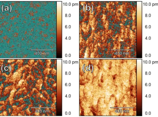
exciting Vac. Figure7presents the corrected d33map of AlN film deposited with – 100 V bias, together with the line-cut indicated by white line in Fig.7a.
One can observe in Fig7b that in some regions the obtained d33data approach the bulk AlN value of 5.6 pm/V [39]. This finding is probably the manifestation of (002) preferential growth.
The corrected average piezoelectric coefficient, DZ ratio, deposition rate, grain size (EDR), and surface roughness (RMS) as a function of applied substrate bias are summarized in Fig.8. The increasing ten- dency of grain size with bias may be associated with the increasing energy transferred by the bom- bardment to the adatoms on the sample surface, which results in larger surface diffusion length, thus larger grain size. However, the reason of the change in deposition rate is still unclear. For comparison, the piezoelectric coefficients measured by Berlin- court method are also presented in Fig.8e. We note that Si also has been used as substrate in the case of -100 V bias. The values measured by Berlincourt method on Ni, and Si substrate are 2.42, and 1.2 pC/N, respectively, which shows the superiority of Ni substrate. As shown by Fig.8, the - 100 V bias voltage is proved to be the best value, which
produced the highest effective coefficient with high deposition rate, and large grain size. There is a fair matching between PFM and piezometer results indicating that using proper probe and correction on reference sample, PFM can be a suitable tool for the investigation of piezoelectric materials in nanoscale.
3.5 Texture of the films
As mentioned in the introduction section, the energy deposition via the impact of the charged particles accelerated by the electric field of the substrate bias on the sample surface promotes the adatom mobility, which can moves to the lowest energy sites to build in. In the case of unbiased sample, however, the kinetic energy of sputtered particles is low, because they have collided once or more times on other par- ticles in plasma due to long target to substrate dis- tance in our case. What is more, a high number of AlN dimers can be formed via collisions in plasma Fig. 7 Corrected d33 map of AlN film deposited at - 100 V
substrate bias (a), and a characteristic line-cut (b) along the white line. Dashed line indicates the d33piezoelectric coefficient of bulk AlN
10 12 14
30 40
12 14 16
0 20 40 60 80 100
0 1 2 3 0 30 60
(a)
(b)
DZ ratio (%) Dep. rate (nm/min.) RMS (nm)Size EDR (nm)
(c)
dav. (pm/V)
(e)
VS (-V) (d)
Fig. 8 Deposition rate (a), grain size (equivalent disk radius) (b), surface roughness (RMS) (c), dead zone ratio (d), and corrected average piezoelectric coefficient (e) as a function of substrate bias voltage. Piezoelectric coefficient measured by macroscopic method (Piezometer) also shown in (e) for comparison (green dots)
with the bond similar to one kind (B1 bond) of those linking the (101) planes [43, 44]. Both low surface mobility as well as formation of AlN dimers are favored for growth in [101] direction as shown by XRD in Fig.9. The (101) plane is semipolar, and its quality in the present case may be low due to low surface mobility of adatoms. Therefore, the piezore- sponse of AlN layer is inferior, as shown by PFM (Fig.3). As the bias voltage increases, the enhanced surface diffusion promotes the formation of smaller energy bonds (B2), thus initiates the growth of (103) and (002) plans, which have low surface energy. The higher surface mobility also promotes the formation of lager grain, smoother surface. According to XRD scans (Fig.9), the dominating texture for all AlN layer deposited with substrate bias is (103) plane, which is about 12 degrees off to the (002) one in AlN single crystal structure, so-called semipolar crystal- lographic plane. The growth of (103) and (002) con- tributes to the improvement of the piezoelectric properties of AlN layer. However, the dominating presence of semipolar (103) plane, and the possibility of defects created by ion bombardment may cause the low effective piezoelectric efficient compared to bulk value.
4 Conclusion
The effect of substrate bias during sputtering depo- sition of AlN layers on rolled Ni sheets has been investigated by means of semi-contact AFM and contact PFM modes. Using non-piezoelectric SiO2
sample the probe with high cantilever spring con- stant (42 N/m) was demonstrated to eliminate the contribution of electrostatic force in piezoelectric response, thus making the PFM results reliable. It has been shown that, without proper energy supply (Vbias
= 0V), the layer consists mostly of dead zones, whose piezoresponse is the same like the background level determined by fitting the piezoresponse at various Vacvalues. The ratio of the dead zone decreases and the homogeneity of the piezoresponse is better as the supplied energy via substrate bias increases indicat- ing a crystal growth in a better preferential direction, which was confirmed by XRD results. As a conse- quence, the effective piezoelectric coefficient mea- sured on the layer increases. Using Z-cut LiNbO3
single crystal as a reference a correction factor of 2.12 was calculated. The corrected average values are in fair agreement with that measured by macroscopic method (Piezometer). The obtained high spatial res- olution d33map proves that using a proper probe and correction on a reference sample off-resonant PFM technique is a powerful quantitative technique for the investigation of piezoelectric materials in nanoscale.
The best average coefficient value achieved at -100V substrate bias is 3.3 pm/V indicating the feasibility of substrate bias assisted AlN deposition on rolled Ni sheet for vibrational energy harvesting applications.
Acknowledgements
This work was supported by the National Research, Development and Innovation Fund of the Hungarian Government in the framework of KoFAH, NVKP_16- 1-2016-0018. The authors thank Levente Ille´s for thickness measurement by SEM, and Erika Tunyogi for assistance in PFM evaluation. J. R. acknowledges the support of the New National Excellence Program of the Ministry for Innovation and Technology, U´ NKP-19-3-III-OE-51.
Open Access This article is licensed under a Crea- tive Commons Attribution 4.0 International License, which permits use, sharing, adaptation, distribution 10
20
10 20
10 20
30 40 50 60
10 20
-100V
-70V
-50V
Lin (counts) NiNi
-0V
(103)
(002) (101)
2Θ (deg)
Fig. 9 XRD patterns of AlN films deposited using different substrate bias
and reproduction in any medium or format, as long as you give appropriate credit to the original author(s) and the source, provide a link to the Crea- tive Commons licence, and indicate if changes were made. The images or other third party material in this article are included in the article’s Creative Commons licence, unless indicated otherwise in a credit line to the material. If material is not included in the article’s Creative Commons licence and your intended use is not permitted by statutory regulation or exceeds the permitted use, you will need to obtain permission directly from the copyright holder. To view a copy of this licence, visit http://creativecommons.org/licen ses/by/4.0/.
Funding
Open access funding provided by ELKH Wigner Research Centre for Physics..
References
1. F. Narita, M. Fox, A review on piezoelectric, magnetostric- tive, and magnetoelectric materials and device technologies for energy harvesting applications. Adv Eng. Mater. (2017).h ttps://doi.org/10.1002/adem.201700743
2. V. Mortet, M. Nesladek, K. Haenen, A. Morel, M. D’Olies- laeger, M. Vanecek, Physical properties of polycrystalline aluminium nitride films deposited by magnetron sputtering.
Diamond Relat. Mater. 13, 1120 (2004). https://doi.org/10.
1016/j.diamond.2003.10.082
3. R. Rodriguez-Clemente, B. Aspar, N. Azema, B. Armas, C.
Combescure, J. Durand, A. Figueras, Morphological proper- ties of chemical vapour deposited AlN films. J. Cryst. Growth 133, 59 (1993).https://doi.org/10.1016/0022-0248(93)90103- 4
4. A. Kakanakova-Georgieva, D. Nilsson, E. Janze, High-qual- ity AlN layers grown by hot-wall MOCVD at reduced tem- peratures. J. Cryst. Growth338, 52 (2012).https://doi.org/10.
1016/j.jcrysgro.2011.10.052
5. S. Karmann, H.P.D. Schenk, U. Kaiser, A. Fissel, Wo.
Richter. , Growth of columnar aluminum nitride layers on Si(111) by molecular beam epitaxy. Mater. Sci. Eng. B 50(1–3), 228–231 (1997).https://doi.org/10.1016/S0921-510 7(97)00168-2
6. P. Verardi, M. Dinescu, C. Gerardi, L. Mirenghi, V. Sandu, AlN thin films deposition by laser ablation of Al target in nitrogen reactive atmosphere. Appl. Surf. Sci. 109–110,
371–375 (1997). https://doi.org/10.1016/S0169-4332(96)007 51-9
7. M. Alevli, C. Ozgit, I. Donmez, N. Biyikli, Structural prop- erties of AlN films deposited by plasma-enhanced atomic layer deposition at different growth temperatures. Phys. Stat.
Sol. A 209(2), 266 (2012). https://doi.org/10.1002/pssa.
201127430
8. G.F. Iriarte, J.G. Rodrıguez, F. Calle, Synthesis of c-axis oriented AlN thin films on different substrates: A review.
Mater. Res. Bull.45, 1039 (2010).https://doi.org/10.1016/j.
materresbull.2010.05.035
9. H. Jin, B. Feng, S. Dong, C. Zhou, J. Zhou, Y. Yang, T. Ren, J. Luo, D. Wang, Influence of substrate temperature on structural properties and deposition rate of AlN thin film deposited by reactive magnetron sputtering. J. Elect. Mater.
41, 1948 (2012).https://doi.org/10.1007/s11664-012-1999-4 10. A. Kale, R.S. Brusa, A. Miotello, Structural and electrical
properties of AlN films deposited using reactive RF mag- netron sputtering for solar concentrator application. Appl.
Surf. Sci.258, 3450 (2012).https://doi.org/10.1016/j.apsusc.
2011.11.095
11. M. Akiyama, K. Nagao, N. Ueno, H. Tateyama, T. Yamada, Influence of metal electrodes on crystal orientation of alu- minum nitride thin films. Vacuum74, 699 (2004).https://doi.
org/10.1016/j.vacuum.2004.01.052
12. M. Clement, L. Vergara, J. Sangrador, E. Iborra, A. Sanz- Herva´s, SAW characteristics of AlN films sputtered on silicon substrates. Ultrasonics42, 403 (2004).https://doi.org/10.101 6/j.ultras.2004.01.034
13. G.F. Iriarte, J. Bjurstro¨m, J. Westlinder, F. Engelmark, I.V.
Katardjiev, Synthesis of C-axis-oriented AlN thin films on high-conducting layers: Al, Mo, Ti, TiN, and Ni. IEEE Trans.
Ultra. Ferro. Freq. Cont.52, 1170 (2005)
14. A. Sanz-Herva´s, L. Vergara, J. Olivares, E. Iborra, Y. Morilla, J. Garcı´a-Lo´pez, M. Clement, J. Sangrador, M.A. Respaldiza, Diamond & Related Mater.14, 1198 (2005).https://doi.org/
10.1016/j.diamond.2004.11.010
15. L. Monteagudo-Lerma, S. Valdueza-Felip, A. Nu´n˜ez-Casca- jero, M. Gonza´lez-Herra´ez, E. Monroy, F.B. Naranjo, Two- step method for the deposition of AlN by radio frequency sputtering. Thin Solid Films545, 149 (2013).https://doi.org/
10.1016/j.tsf.2013.07.062
16. J. Wang, Q. Zhang, G.F. Yang, C.J. Yao, Y.J. Li, R. Sun, J.L.
Zhao, S.M. Gao, Effect of substrate temperature and bias voltage on the properties in DC magnetron sputtered AlN films on glass substrates. J. Mater. Sci: Mater. Electron.
(2015).https://doi.org/10.1007/s10854-015-4125-6
17. F. Wang, F. Xiao, D. Song, L. Qian, Y. Feng, B. Fu, K. Dong, C. Li, K. Zhang, Research of micro area piezoelectric prop- erties of AlN films and fabrication of high frequency SAW
devices. Microelect. Eng.199, 63 (2018).https://doi.org/10.
1016/j.mee.2018.07.016
18. I. Kanno, Piezoelectric MEMS for energy harvesting.
J. Phys.: Conf. Series660, 012001 (2015).https://doi.org/10.
1088/1742-6596/660/1/012001
19. J. Yang, X. Jiao, R. Zhang, H. Zhong, Y. Shi, B. Du, Growth of AlN films as a function of temperature on Mo films deposited by different techniques. J. Elect. Mater. 43, 369 (2014).https://doi.org/10.1007/s11664-013-2867-6
20. F. Medjani, R. Sanjine´s, G. Allidi, A. Karimi, Effect of sub- strate temperature and bias voltage on the crystallite orienta- tion in RF magnetron sputtered AlN thin films. Thin Solid Films515, 260 (2006).https://doi.org/10.1016/j.tsf.2005.12.
145
21. R.E. Taylor, CINDAS Data Series on Materials Properties, Thermal Expansion of Solids,Vol 1–4, ASM Int. (1998) 22. G.A. Slack, S.F. Bartram, Thermal expansion of some dia-
mondlike crystals. J. Appl. Phys.46, 89–98 (1975).https://d oi.org/10.1063/1.321373
23. A.K. Chu, C.H. Chao, F.Z. Lee, H.L. Huang, Influences of bias voltage on the crystallographic orientation of AlN thin films prepared by long-distance magnetron sputtering. Thin Solid Films429, 1 (2003).https://doi.org/10.1016/S0040-60 90(02)01286-5
24. H. Suharyadi, The influence of substrate bias and sputtering pressure on the deposited aluminium nitride for magneto- electric sensors. J. Phys.: Conf. Series1517, 012104 (2020).h ttps://doi.org/10.1088/1742-6596/1517/1/012104
25. C.S. Sandu, F. Parsapour, D. Xiao, R. Nigon, L.M. Riemer, T.
LaGrange, P. Muralt, Impact of negative bias on the piezo- electric properties through the incidence of abnormal oriented grains in Al0.62Sc0.38N thin films. Thin Sol. Film697, 137819 (2020).https://doi.org/10.1016/j.tsf.2020.137819
26. M. Ohring,The Materials Science of Thin Films(Academic Press Inc, San Diego, California, 1992)
27. D. Berlincourt, H. Jaffe, Elastic and piezoelectric coefficients of single-crystal barium titanate. Phys. Rev.111, 143 (1958).
https://doi.org/10.1103/PhysRev.111.143
28. M. Al Ahmad, R. Plana, Piezoelectric coefficients of thin film aluminum nitride characterizations using capacitance mea- surements. IEEE Microw. Wirel. Compon. Lett. 19, 140 (2009).https://doi.org/10.1109/LMWC.2009.2013682 29. A. Ababneh, U. Schmid, J. Hernando, J.L. Sa´nchez-Rojas, H.
Seidela, The influence of sputter deposition parameters on piezoelectric and mechanical properties of AlN thin films.
Mater. Sci. Eng. B172, 25 (2010).https://doi.org/10.1016/j.
mseb.2010.05.026
30. T. Kamohara, M. Akiyama, N. Kuwano, Influence of polar distribution on piezoelectric response of aluminum nitride
thin films. Appl. Phys. Lett.92, 093506 (2008).https://doi.
org/10.1063/1.2892041
31. M. Reusch, K. Holc, W. Pletschen, L. Kirste, A. Zˇ ukauskait_e, T. Yoshikawa, D. Iankov, O. Ambacher, V. Lebedev, Analysis and optimization of sputter deposited AlN-layers for flexural plate wave devices. J. Vac. Sci. Technol. B 34, 052001 (2016).https://doi.org/10.1116/1.4959580
32. B.J. Rodriguez, C. Callahan, S.V. Kalinin, R. Proksch, Dual- frequency resonance-tracking atomic force microscopy.
Nanotechnology18, 475504 (2007).https://doi.org/10.1088/
0957-4484/18/47/475504
33. S. Jesse, S.V. Kalinin, R. Proksch, A.P. Baddorf, B.J.
Rodriguez, The band excitation method in scanning probe microscopy for rapid mapping of energy dissipation on the nanoscale. Nanotechnology18, 435503 (2007).https://doi.or g/10.1088/0957-4484/18/43/435503
34. S.V. Kalinin, B.J. Rodriguez, S. Jesse, K. Seal, R. Proksch, S.
Hohlbauch, I. Revenko, G.L. Thompson, A.A. Vertegel, Towards local electromechanical probing of cellular and biomolecular systems in a liquid environment. Nanotechnol- ogy18, 424020 (2007).https://doi.org/10.1088/0957-4484/1 8/42/424020
35. N. Balke, S. Jesse, P. Yu, B. Carmichael, S.V. Kalinin, A.
Tselev, Quantification of surface displacements and elec- tromechanical phenomena via dynamic atomic force micro- scopy. Nanotechnology27, 425707 (2016).https://doi.org/10.
1088/0957-4484/27/42/425707
36. D. Necˇas, P. Klapetek, Gwyddion: an open-source software for SPM data analysis. Centr. Eur. J. Phys.10, 181 (2012).h ttps://doi.org/10.2478/s11534-011-0096-2
37. N. Balke, S. Jesse, Q. Li, P. Maksymovych, M.B. Okatan, E.
Strelcov, A. Tselev, S.V. Kalinin, Current and surface charge modified hysteresis loops in ferroelectric thin films. J. Appl.
Phys.118, 072013 (2015).https://doi.org/10.1063/1.4927811 38. D. Seol, B. Kim, Y. Kim, Review: non-piezoelectric effects in piezoresponse force microscopy. Current Appl. Phys.17, 661 (2017).https://doi.org/10.1016/j.cap.2016.12.012
39. I.L. Guy, S. Muensit, E.M. Goldys, Extensional piezoelectric coefficients of gallium nitride and aluminum nitride. Appl.
Phys. Lett.75, 4133–4135 (1999).https://doi.org/10.1063/1.
125560
40. K. Lefki, G.J.M. Dormans, Measurement of piezoelectric coefficients of ferroelectric thin films. J. Appl. Phys.76, 1764 (1994).https://doi.org/10.1063/1.357693
41. C.M. Lueng, H.L.W. Chan, C. Surya, C.L. Choy, Piezoelec- tric coefficient of aluminum nitride and gallium nitride.
J. Appl. Phys. 88, 5360 (2000). https://doi.org/10.1063/1.
1317244
42. R.T. Smith, F.S. Welsh, Temperature dependence of the elastic, piezoelectric, and dielectric constants of lithium
tantalate and lithium niobate. J. Appl. Phys.42, 2219 (1971).
https://doi.org/10.1063/1.1660528
43. X. Xu, H. Wu, C. Zhang, Z. Jin, Morphological properties of AlN piezoelectric thin films deposited by DC reactive mag- netron sputtering. Thin Solid Films388, 62 (2001).https://d oi.org/10.1016/S0040-6090(00)01914-3
44. M. Ishihara, S.J. Li, H. Yumoto, K. Akashi, Y. Ide, Control of preferential orientation of AlN films prepared by the reactive
sputtering method. Thin Solid Films316, 152 (1998). http s://doi.org/10.1016/S0040-6090(98)00406-4
Publisher’s Note Springer Nature remains neutral with regard to jurisdictional claims in published maps and institutional affiliations.