Peter Petrik
Characterization of polysilicon thin films using in situ and ex situ spectroscopic
ellipsometry
DISSERTATION
for the degree of
Doctor of Philosophy
in
Physics
Department of Experimental Physics of the Technical University of Budapest
&
Research Institute for Technical Physics and Materials Science of the
Hungarian Academy of Sciences
Budapest, 1999
Acknowledgments
This thesis could not exist without the help of many colleagues at the Research Insti- tute for Technical Physics and Materials Science (MTA-MFA), at the Chair of Electron Devices of the Friedrich-Alexander University Erlangen-Nuremberg (LEB) and at the Fraunhofer Institute for Integrated Circuits (FhG-IIS-B) in Erlangen, Germany. Most of the sample preparations and measurements were made at the LEB and FhG-IIS-B.
Financial support of the Soros Foundation and the DAAD (Deutscher Akademischer Austauschdienst) is gratefully appreciated.
I thank
• Prof. J´ozsef Gyulai, my advisor, for orienting me to a fruitful cooperation with colleagues in Erlangen, and for his constant support during my work,
• Prof. Dr.-Ing. H. Ryssel for the opportunity to contribute to developments and to perform measurements and sample preparations at the LEB and FhG-IIS-B,
• Dr. Tivadar Lohner and Dr. Mikl´os Fried for good ideas, advices, discussions, and continuous support,
• Dr. Claus Schneider, Wolfgang Lehnert, Dr. Rudolf Berger for the lot of help and support during my stays in Erlangen,
• Dr. L´aszl´o P´eter Bir´o and Dr. Nguyen Quoc Kh´anh for fruitful discussions and their contribution to the measurements,
• Oliv´er Polg´ar for the software for ellipsometric data evaluation, Annette Daurer for TEM measurements, and the numerous colleagues at the MTA-MFA, LEB, and FhG-IIS-B for their support.
Special thanks to Dr. Ter´ez Korm´any, who helped me to join a wonderful research group, and Dr. J´anos M¨uller, my teacher at secondary school, who gave me the basic knowledge and the first kick to the direction of natural sciences.
I thank my family, especially my wife ´Eva, who had to miss me during my lengthy absences, for the constant support.
Preface
Spectroscopic ellipsometry (SE) and polysilicon: a key measurement technique and a key material in today’s microelectronics. Ellipsometry is an optical method, which measures the complex reflectance ratio of the sample. The words “optical” and “com- plex” are very important. “Optical” means that it is non-destructive and capable ofin situmeasurements. “Complex” means that not only intensity differences are obtained, as in case of spectrophotometers, but also phase information, allowing sub-monolayer precision. The trend toward smaller device dimensions in the semiconductor industry increased the importance of in situ capability and sub-monolayer precision. Taking CMOS technology as an example, the feature size is currently 250 nm with a gate oxide thickness of 4-5 nm. Feature size and gate oxide thickness are expected to shrink to 70 nm and 1.5 nm, respectively, in 2009 [Cof98]. The recently emerging concept of “single wafer processing”, as well as new techniques to provide optical access to processed wafers will increase the importance of the in situ measurement including SE and other optical methods. The extended analytic capabilities of spec- troscopic instruments lead them to be applied to increasingly complex samples like multilayer coatings, ion implanted materials or other microscopically inhomogeneous materials. Some material and structural properties, which can be measured by SE involve the determination of refractive index (n and k from one measurement), layer thickness (also multilayer stacks), interface quality, microstructure, contamination, surface properties, or profiles in layers with continously varying refractive index. Us- ing photodiode array detectors a data acquisition time of 12 ms per measurement can be achieved, which makes SE especially attractive for real time applications. Although the principles of ellipsometry date back to the late 19th century, based on Drude’s investigations [Dru89a, Dru89b, Dru90], this technique was not used until the begin- ning of 1960s. The reason is that an ellipsometric measurement entails the solution of complicated complex non-linear equations which can be solved analytically only in special cases and require numerical approaches in most instances. The computers of rapidly increasing performance and decreasing prices were the sufficient tools for the data processing.
Understanding and utilizing the advantages of polysilicon was one of the most important fundamental developments in the history of integrated circuits. Polysilicon is widely used because it forms an adherent oxide, adsorbs and re-emits dopants, has good step coverage if deposited by chemical vapor deposition (CVD), matches the mechanical properties of Si single-crystal, has a high melting point, has a compatible work function for MOS devices, absorbs heavy metals (gettering), forms high conduc- tivity silicides, and is compatible with HF. Its compatibility with IC processing and its good step coverage provided by CVD offers many advantages in bipolar, MOS,
and BiCMOS circuits, because it provides low MOS threshold voltage, fills trenches, permits SAliciding, provides long gate oxide wearout times, provides a wide range of resistivities, permits oxide reflow process temperatures, simplifies processing, can be selectively deposited, permits shallow, high quality junctions, and forms silicide thin film resistors. Polysilicon will have applications in semiconductor devices far into the future because it plays major role in the fabrication of all manner of devices.
In the present work ex situ and in situ measurement of polysilicon thin films was performed using spectroscopic ellipsometry. I could take advantage of the high amount of information contained in the measured spectra which has been used for a wide range of investigations targeting polycrystalline silicon.
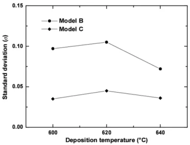
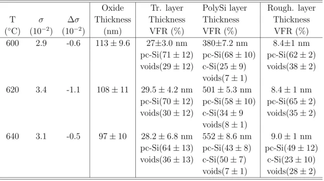
First, optical models were developed in order to provide a good description of the multi-layer structures used in the study. As the properties of polysilicon depend strongly on the preparation conditions, there is no way of using a single reference dielectric function data for the polysilicon layers. Therefore, the polysilicon structure was modeled as a mixture of different phases like single-crystalline silicon, amorphous silicon and voids utilizing the advantages of the Bruggeman effective-medium approx- imation used widely for polysilicon in the literature. I have shown that using these three components does not provide a good description for all deposition conditions.
Using also fine-grained polycrystalline silicon as reference data in the effective medium model results in a better fit of the experimental data and provides an insight of the structural change as a function of deposition temperature or layer thickness.
Using effective medium models surface roughness can be measured quantitatively.
Comparison with results from independent measurement techniques like atomic force microscopy or transmission electron microscopy justifies the reliability of the optical models and the precision of the optical method. An important output of the inves- tigations was that in spite of the good agreement between ellipsometry and atomic force microscopy, care must be taken on the interpretation of the measurement results (explanations in the literature are rather confusing in many cases).
This method can be used even in the very complex cases of ion-implanted single- and polycrystalline silicon. In this case the multilayer models are extended to take into account the damage depth profile as a compositional change in the effective medium model. The reliability of the method has been proven by cross-checking measurements with Rutherford backscattering spectrometry and transmission electron microscopy.
Application of the optical models were demonstrated byin situ measurement in a vertical furnace during annealing of amorphous silicon. At the Fraunhofer Institute for Integrated Circuits in Erlangen, a spectroscopic ellipsometer was integrated in a vertical furnace using a novel beam guiding system. I had the opportunity to take part of the development by realizing a method of the correction for the phase shift of the beam-guiding prisms, and performing measurements in the vertical furnace in order to determine the high temperature reference data and – using these results together with the optical models developed during the ex situ investigations – to monitor the crystallization of amorphous silicon during annealing. We showed that in spite of the rather long beam path and the complicated beam-guiding system the equipment is capable forin situmonitoring of high temperature processes inside a vertical furnace.
The novel method for the integration allows a cheap and fast integration into industrial equipment with minor modification of the chamber itself.
Contents
1 Theory 1
1.1 Basics of ellipsometry . . . 1
1.1.1 Physics . . . 1
1.1.2 Optical model . . . 2
1.1.3 Effective medium theory . . . 8
1.1.4 Instrumentation . . . 13
1.2 Applications of ellipsometry . . . 17
1.2.1 Precision . . . 21
1.3 Chemical vapor deposition . . . 25
1.4 Preparation and applications of polycrystalline silicon . . . 28
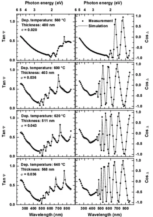
2 Optical models for polycrystalline silicon 33 2.1 Experimental details . . . 34
2.2 Optical models . . . 35
2.3 Model parameters vs. deposition temperature . . . 39
2.4 Model parameters vs. layer thickness . . . 46
3 Microscopic Surface Roughness 53 3.1 Experimental details . . . 54
3.1.1 Brief description of atomic force microscopy . . . 54
3.1.2 Sample preparation and measurements . . . 56
3.2 Results and discussion . . . 57
3.2.1 AFM measurements . . . 57
3.2.2 Ellipsometry measurements . . . 58
3.3 Comparison . . . 60
4 Ion-Implantation of Single- and Polycrystalline Silicon 65 4.1 Experimental details . . . 65
4.1.1 Short description of backscattering spectrometry . . . 65
4.1.2 Sample preparation and measurements . . . 68
4.2 Implantation of single-crystalline silicon . . . 69
4.3 Implantation of polycrystalline silicon . . . 71
5 In situ ellipsometry in vertical furnace 79 5.1 Instrumentation . . . 80
5.2 Measurements using the beam-guiding system . . . 81
5.3 Measurements at high temperature . . . 85
5.4 Annealing of amorphous silicon samples . . . 87
Bibliography 93
List of used acronyms 105
Summary 108
List of relevant publications 111
Chapter 1 Theory
1.1 Basics of ellipsometry
1.1.1 Physics
Ellipsometry measures the change on the state of polarization caused by the reflection on the sample. If polarized light will be reflected on the boundary of two media (see Fig. 1.1), the state of polarization of the reflected beam will be elliptic, circular, or linear depending on the properties of the sample.
The state of polarization can be described by dividing the light beam into two components that are parallel (Ep) and perpendicular (Es) to the plane of incidence (the over-line denotes complex values). Both components are plane waves described by [Bor68]
E =E0ei(ωt+δ)e−iωncr, (1.1)
where ω is the frequency, δ is the phase, n =n−ik is the complex refractive index, and c is the speed of the light in vacuum. The state of polarization of a plane wave is defined by
χ= Ep
Es. (1.2)
where p and s denote the components parallel and perpendicular to the plane of incidence respectively, and χ is called the polarization coefficient. An ellipsometric measurement provides the ratio of the polarization coefficients of the reflected (χr) and incident (χi) light:
ρ= χr
χi. (1.3)
In the late 19th century Drude [Dru89a, Dru89b] introduced the following termi- nology:
ρ= χr
χi = |χr|
|χi|ei(δr−δi) = tan Ψei∆. (1.4) The ratio of the polarization coefficients is equivalent with the ratio of the Fresnel-
reflection coefficients rp and rs: χr χi =
Er,p
Er,s
Ei,p
Ei,s
=
Er,p
Ei,p
Er,s
Ei,s
= rp
rs, (1.5)
consequently,ρ is called the complex reflectance ratio.
TanΨ and ∆ can be written as
tan Ψ = |χr|
|χi| = |rp|
|rs|, (1.6)
and
∆ =δr−δi = (δr,p−δr,s)−(δi,p−δi,s) = (δr,p−δi,p)−(δr,s−δi,s) = ∆p−∆s, (1.7) where δ denotes the phase of the components (i: incident, r: reflected, p: parallel, s: perpendicular). TanΨ is the ratio of the absolute values of the reflected and incident polarization components, or equivalently, the ratio of the absolute values of thepand scomponents of the Fresnel-reflection coefficients. The values Ψ and ∆ are called the ellipsometric angles.
Using the photometric method, cos∆ is directly obtained from the line shape analysis (see Section 1.1.4, page 14). For spectroscopic ellipsometry, the convention of plotting the tanΨ and cos∆ values is used, rather than plotting the Ψ and ∆ values as in the case of single wavelength ellipsometry. The reason is, that most of the spectroscopic ellipsometers use the photometric method.
1.1.2 Optical model
The determination of the physical parameters (layer thickness, refractive index, mi- crostructure, etc.) of the sample from the measured values (tanΨ–cos∆ or Ψ–∆) depends on three factors [Asp82]:
• accurate spectroscopic data for the sample and its possible constituents,
• an appropriate model for the complex reflectancesrp and rs expressed in terms of the sample microstructure,
• the systematic, objective determination of the values and confidence limits of the wavelength-independent parameters of the model with linear regression analysis.
Surprisingly, the first requirement is not trivial. Not because of instrumentation limitations, but because optical measurements, particularly ellipsometric measure- ments, are extremely sensitive to surface conditions. To lowest order everyone takes accurate data, but the extent to which these data accurately represent the intrin- sic properties of a sample depends on how well the model assumptions are realized in practice. For example, the accuracy of dielectric function data for a homogeneous ma- terial with a nominally bare surface depends on how completely unwanted over-layer material can be removed.
The second requirement demands some physical insight into the possible structure of the sample, i. e. whether intrinsic over-layers such as density-deficient outer regions
1.1 Basics of ellipsometry 3
Φ1
Φ0 Φ0
p s
p s
s p
s p
Medium 0 Medium 1
Plane of incidence Plane of sample
Figure 1.1. Reflexion of polarized light
are likely to be present, whether the heterogeneity is macroscopically isotropic, etc. If a microstructurally heterogeneous material consists of regions large enough to possess their own dielectric identity, the samples can be described in terms of multilayer models and effective-medium theory (see Section 1.1.3). These models allow the response of the sample to be described by a few wavelength-independent parameters such as compositions, thicknesses, or densities, which contain the microstructural information about the sample. These are analogous to the frequency-independent lumped-circuit resistance, capacitance, and inductance parameters of circuit theory.
The third requirement deals with the determination of these parameters by linear regression analysis (LRA). While the principal purpose of LRA is to provide least- squares values, an equally important function is to provide confidence limits on the values themselves. The confidence limits not only give some insight as to how well a particular model fits the data, but they also provide information as to whether the data are really determining parameter values, or whether too many parameters have been used. Too many parameters, or correlated parameters, result in drastic increase in the confidence limits. They thereby provide a natural check against the tendency to add parameters indiscriminately simply for the sake of reducing the mean-square deviation.
Most optical models use flat semi-infinite substrates with one or more laminar adherent layers of uniform thickness on the surface. The mathematical description of the interaction between light and material is given by Maxwell’s equations. Based on these equations, the Fresnel-reflection coefficients can be calculated. The simplest case is the reflection and transmission at the planar interface between two isotropic media (see Fig. 1.1).
In this case, the Fresnel-reflection coefficients can be written as [Azz87]
Er,p
Ei,p =rp = n1cos Φ0−n0cos Φ1
n1cos Φ0+n0cos Φ1, (1.8) Er,s
Ei,s =rs = n0cos Φ0−n1cos Φ1 n0cos Φ0+n1cos Φ1
, (1.9)
wheren0 is the refractive index of Medium 0 (see Fig. 1.1),n1 is the refractive index of Medium 1, Φ0 is the angle of incidence, and Φ1 is the angle of refraction. Φ1 can be obtained using
n0sin Φ0 =n1sin Φ1, (1.10)
Ambient (0)
Φ1
Φ0
Φ2 Film (1)
Su
bstrate (2) d1
Figure 1.2. Multiple reflexion in a three-phase system
which is Snell’s law.
Thus ρcan be expressed by the refractive indices and the angle of incidence:
ρ= rp
rs =ρ(n0, n1,Φ0). (1.11) n1 can be calculated, because Φ0 and n0 are known (n0 = 1 if Medium 0 is air).
A case of considerable importance in ellipsometry is that in which polarized light is reflected from, or transmitted by a substrate covered by a single film (see Fig. 1.2).
A plane wave incident in Medium 0 (at an angle Φ0) will give rise to a resultant reflected wave in the same medium and to a resultant transmitted wave (at the angle Φ2) in Medium 2 (the substrate). Our objective is to relate the complex amplitudes of the resultant reflected and transmitted waves to the amplitude of the incident wave, when the latter is linearly polarized parallel (p) and perpendicular (s) to the plane of incidence. Addition of the partial waves leads to an infinite geometric series for the total reflected amplitude R
Rj = rj01+rj12e−iβ
1 +rj01rj12e−iβ, j =p, s, (1.12) wherer01 and r12 are the reflection coefficients at the 0|1 (1|0) and 1|2 interfaces. In terms of the free-space wavelength λ, the film thickness d1, the film complex index of refraction n1 and the angle of refraction in the film Φ1, the phase angle β (film phase thickness, i. e. the phase change that the multiply-reflected wave inside the film experiences as it traverses the film once from one boundary to the other) is given by
β = 2π(d1
λ)n1cos Φ1, (1.13)
or
β = 2π(d1
λ)n1qn21−n20sin Φ0, (1.14) if Snell’s law (eqn. 1.10) is applied, where Φ0 is the angle of incidence in Medium 0.
The method of addition of multiple reflections becomes impractical when con- sidering the reflection and transmission of polarized light at oblique incidence by a multilayer film between semi-infinite ambient and substrate media. A more elegant
1.1 Basics of ellipsometry 5
Φ0
Φm+1
Φj
1 2
j
m
m+1 (substrate) 0 (ambient) Y X
Z
Figure 1.3. Reflection and transmission of a plane wave by a multi-film structure (films 1, 2,
· · ·, m) sandwiched between semi-infinite ambient (0) and substrate (m+1) media. Φ0 is the angle of incidence, Φj and Φm+1 are the angles of refraction in the jth film and substrate, respectively.
approach is to employ 2× 2 matrices [Azz87]. This method is based on the fact that the equations that govern the propagation of light are linear and that the continuity of the tangential fields across an interface between two isotropic media can be regarded as a 2 ×2 – linear-matrix transformation.
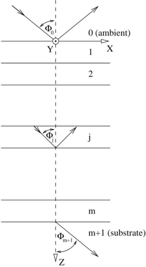
Consider a stratified structure that consists of a stack of 1,2,3,· · ·, j,· · ·, m par- allel layers sandwiched between semi-infinite ambient (0) and substrate (m+1) media (Fig. 1.3). Let all media be linear homogeneous and isotropic, and let the complex index of refraction of thejth layer benj and its thickness dj. n0 andnm+1 represents the complex indices of refraction of the ambient and substrate media, respectively.
An incident monochromatic plane wave in Medium 0 (the ambient) generates a re- sultant reflected plane wave in the same medium and a resultant transmitted plane wave in medium m+1 (the substrate). The total field inside thejth layer consists of a forward- and a backward-traveling plane wave denoted by “+” and “−”, respectively.
LetE+(z) andE−(z) denote the complex amplitudes of the forward- and backward- traveling plane waves at an arbitrary plane z. The total field at z can be described by a 2×1 column vector
E(z) =
"
E+(z) E−(z)
#
. (1.15)
If we consider the fields at two different planes z0 and z00 parallel to the layer boundaries then, by virtue of system linearity, E(z00) andE(z0) must be related by a
2×2-matrix transformation
"
E+(z0) E−(z0)
#
=
"
S11 S12 S21 S22
#"
E+(z00) E−(z00)
#
, (1.16)
or more concisely,
E(z0) = S E(z00), (1.17) where
S =
"
S11 S12
S21 S22
#
. (1.18)
By choosingz0 andz00 to lie immediately on opposite sides of the (j−1)|j interface, located atzj between layers j−1 and j, equation 1.17 becomes
E(zj −0) = I(j−1)jE(zj + 0), (1.19)
where I(j−1)j is a 2×2 matrix characteristic of the (j −1)|j interface alone. On the other hand, if z0 and z00 are chosen inside the jth layer at its boundaries, eqn. 1.17 becomes
E(zj+ 0) =LjE(zj+dj −0), (1.20) where Lj is a 2×2 matrix characteristic of the jth layer alone whose thickness is dj. Only the reflected wave in the ambient medium and the transmitted wave in the substrate are accessible for measurement, so that it is necessary to relate their fields to those of the incident wave. By taking the planesz0 andz00 to lie in the ambient and substrate media, immediately adjacent to the 0|1 andm|(m+1) interfaces respectively, eqn. 1.17 will read
E(z1−0) =S E(zm+1+ 0). (1.21) Equation 1.21 defines a scattering matrixS which represents the overall reflection and transmission properties of the stratified structure. Scan be expressed as a product of the interface and layer matrices I and Lthat describe the effects of the individual interfaces and layers of the entire stratified structure, taken in proper order, as follows:
S =I01L1I12L2· · ·I(j−1)jLj· · ·LmIm(m+1). (1.22) Equation 1.22 may be proved readily by repeated application of eqn. 1.17 to the successive interfaces and layers of the stratified structure, starting with the ambient- first film (0|1) interface and ending by the last film-substrate interface [m|(m+ 0)].
As an example, consider the case of a single film (1) sandwiched between semi- infinite ambient (0) and substrate (2) media (Fig. 1.2). From eqn. 1.22 the scattering matrix S in this case is given by
S =I01L1I12, (1.23)
which upon substitution ofI01,L1 and I12 [Azz87] becomes S = ( 1
t01t12)
"
1 r01 r01 1
#"
ejβ 0 0 e−jβ
#"
1 r12 r12 1
#
. (1.24)
1.1 Basics of ellipsometry 7
In case of a two film system, eqs. 1.23 and 1.24 only have to be extended as S =I01L1I12L2I23, (1.25) and
S = ( 1 t01t12)
"
1 r01 r01 1
#"
ejβ1 0 0 e−jβ1
#"
1 r12 r12 1
#"
ejβ2 0 0 e−jβ2
#"
1 r23 r23 1
#
. (1.26) If we consider the overall system as a two-phase (ambient-substrate) structure, then eqn. 1.16 can be rewritten as
"
E+a E−a
#
=
"
S11 S12 S21 S22
#"
E+s 0
#
, (1.27)
where the subscripts a and s refer to the ambient and substrate media, respectively, and E−s = 0. Further expansion of eqn. 1.27 yields the overall reflection and trans- mission coefficients of the stratified structures as
R= E−a
E+a = S21
S11, (1.28)
T = E+s E+a = 1
S11, (1.29)
respectively. From eqs. 1.28 and 1.29 it is clear that only elements of the first column of scattering matrix S determine the overall reflection and transmission coefficients.
Then ρ can be expressed by the overall (effective) reflection coefficients (Rp and Rs):
ρ= Rp
Rs. (1.30)
The number of the parameters is much higher than for a two phase system:
ρ=ρ(n0, n1,· · ·, nm, d1, d2,· · ·, dk,Φ0, λ). (1.31) To determine the unknown parameters one has to increase the amount of indepen- dent information. There are several possibilities, e. g. multiple angles of incidence, different ambients, and different layer thickness of the same material. The most im- portant is the multi-wavelength approach (spectroscopic ellipsometry or SE).
The complex non-linear function standing on the right-hand side of eqn. 1.31 can be inverted only in special cases. A general solution is provided by using the LRA technique to minimize the differences between the calculated and experimental data by adjusting the model parameters, and finally to obtain the results in terms of best-fit model parameters and their 95% confidence limits as well as the unbiased estimator σ of the mean square deviation,
σ =
v u u t
1 (N −P −1)
n
X
j=1
{(cos ∆measj −cos ∆calcj )2+ (tan Ψmeasj −tan Ψcalcj )2}, (1.32)
where N is the number of independent readings corresponding to the different wave- lengths at which SE measurements are made, P is the number of unknown model parameters, and tanΨ and cos∆ are the measured (“meas”) or calculated (“calc”) ellipsometric values.
1.1.3 Effective medium theory
The objective of effective medium theory is to determine the dielectric function of macroscopically homogeneous and microscopically heterogeneous or composite mate- rials. Examples of composite materials include metal films, which can be described as a heterogeneous mixture of materials and voids owing to the inability of form- ing grain boundaries in closely packed systems without some loss of material. Other examples include polycrystalline films, amorphous materials and glasses. A micro- scopically rough surface can also be considered as a heterogeneous medium, being a mixture of bulk and ambient on a microscopic scale. The material can be considered as macroscopically homogeneous, if the dimensions of the phases are smaller than the wavelength of the measuring light.
The dielectric function of a heterogeneous material and the limits to the amount of microstructural information that can be drawn from it are easily understood if we recall that electrodynamics deals with macroscopic observables that are basically av- erages of their microscopic counterparts. Therefore, the solution involves two distinct steps: first, the electrostatic problem is solved exactly for a given microstructure to obtain the local electric field ~e(~r) and dipole moment ~p(~r) per unit volume at ev- ery point in space; secondly, these microscopic solutions are averaged to obtain their macroscopic counterpartsE~ and P~ [Asp82]. The dielectric function of a material is defined as
D~ = ~E =E~ + 4π ~P , (1.33) where D,~ E, and~ P~ are the macroscopic (average or observable) displacement field, electric field, and dipole moment per unit volume, respectively.
To calculate the local electric field, a simple approach is the exactly solvable config- uration where a simple cubic lattice of points with lattice constantsaand polarizability α(the Clausius-Mosotti model) is considered. This is the prototypical inhomogeneous material, being a mixture of polarizable points and empty space. If a uniform fieldE~i is applied, the points polarize as ~p = α ~Eloc, where E~loc =~e(R~n) is the local field at a lattice siteR~n. The microscopic field~e(~r) is the superposition of E~i and the dipole fields from~p and can be written
~e(~r) =E~i+X
Rn
E~dip(~r−R~n), (1.34) where
E~dip(~r) = 3(~p~r)~r−~p ~r2
r5 . (1.35)
Because dipoles occur only on lattice sites and all~e(R~n) are equal:
~
p(~r) =X
Rn
α~e(0)δ(~r−R~n). (1.36)
1.1 Basics of ellipsometry 9
If eqs. 1.34 and 1.35 are valid everywhere, they are certainly valid at~r= 0, so
~e(0) =E~i+ X
Rn6=0
E~dip(R~n). (1.37) Equation 1.37 is a self-consistency relation between ~e(0) = E~loc and E~i. For full cubic symmetry the sum over R~n vanishes and we have simply E~i = E~loc. However, this is not generally true for systems of lower symmetry, such as molecules adsorbed on a surface.
We now have an exact microscopic solution and can proceed to the second step, i. e. averaging the microscopic solutions to obtain their macroscopic counterpart.
Eqn. 1.36 can be averaged to
P~ = N
V α ~Eloc=nα ~Eloc, (1.38) where V is the volume of the sample and n = a−3 is the volume density of points.
The volume average of~e(~r) is slightly more complicated because the volume integral of a dipole field is not zero, but −4π3 . Using this result, we find from eqn. 1.34 the average or macroscopic field to be
E~ =E~loc(1− 4π
3 nα). (1.39)
Therefore the uniform microscopic field E~i = E~loc that was actually applied is larger than the uniform macroscopic field E~ that was apparently applied because the induced dipoles oppose on the average the applied field. After some algebra, all fields can be eliminated from eqs. 1.33, 1.38, and 1.39 and we obtain the Clausius-Mosotti result
−1 + 2 = 4π
3 nα. (1.40)
This model shows the connections among microstructure and microscopic and macroscopic fields and polarizations.
The dielectric function of a heterogeneous medium can be calculated when the points in the preceeding example are assigned different polarizabilities. The simplest case is the random mixture of two materials with polarizabilities αa and αb:
−1 + 2 = 4π
3 (naαa+nbαb), (1.41) where is now the effective dielectric function of the composite. This form involves microstructural parameters that are not measured directly. But if the dielectric func- tionsaandbof phasesaandb are available, we can use eqn. 1.40 to rewrite eqn. 1.41 as
−1
+ 2 =faa−1
a+ 2 +fbb−1
b+ 2, (1.42)
wherefa=na/(na+nb) andfb =nb/(na+nb) are the volume fractions of the phases a and b. This is the Lorentz-Lorenz effective medium expression [Lor80, Lor16].
Let us suppose next that the separate phases a and b are not mixed on an atomic scale but rather consist of regions large enough to possess their own dielectric identity.
Then the assumption of vacuum ( = 1) as the host medium in which to embed points is not good. If we suppose that the host dielectric function ish, then eqn. 1.42 becomes
−h + 2h =fa
a−h a+ 2h +fb
b−h
b + 2h. (1.43)
Specifically, if b represents the dilute phase then we should choose h = a, in which case
−a
+ 2a =fb b−a
b+ 2a. (1.44)
Equation 1.44 and the alternative equation obtained withh =b are the Maxwell- Garnett effective medium expressions [MG04].
In cases wherefa andfb are comparable, it may not be clear whethera orb is the host medium. One alternative is simply to make the self-consistent choiceh =, in which case eqn. 1.43 reduces to
0 =fa
a− a+ 2 +fb
b−
b+ 2. (1.45)
This is the Bruggeman expression, commonly called the Bruggeman effective- medium approximation (B-EMA) [Bru35]. Although they are related, eqn. 1.44 ac- tually describes a coated-sphere microstructure where a is completely surrounded by b, while eqn. 1.45 refers to the aggregate or random-mixture microstructure where a and b are inserted into the effective medium itself.
What happens if the microstructure is not point like (spherically symmetric) as assumed previously? Let us suppose that all internal boundaries are parallel to the applied field, as in a laminar sample with the field applied parallel to the layers. The boundary condition on tangentialE~ shows that the field is uniform everywhere. The polarization is then simply proportional to a orb, according to whether~r is located ina or b. Averaging everything leads to
=faa+fbb, (1.46)
a simple volume average equivalent to capacitors connected in parallel. IfE~ is applied perpendicular to the layers, then D~ is uniform throughout and averaging now leads to
1 = fa
a + fb
b, (1.47)
equivalent to capacitors connected in series.
Equations 1.46 and 1.47 are the Wiener absolute bounds to . They are absolute because no matter what the microstructure there can never be less screening than no screening (all boundaries parallel to the field, eqn. 1.46) nor more screening than maximum screening (all boundaries perpendicular to the field, eqn. 1.47). For any composition and microstructure, must lie on or within the region in the complex plane enclosed by eqs. 1.46 and 1.47 as long as the microstructural dimensions
1.1 Basics of ellipsometry 11
remain small compared with the wavelength of light. The Wiener bounds are easy to construct since eqn. 1.46 is a straight line betweena and b while eqn. 1.47 is a circle passing through a, b, and 0.
Screening is taken into account if eqn. 1.43 is modified to −h
+yh =fa
a−h
a+yh +fb
b−h
b+yh, (1.48)
where y = (1/l)−1, 0 ≤ l ≤ 1, l is the screening parameter. Eqn. 1.48 reduces to eqn. 1.46 or 1.47 for l = 0 (no screening) or l = 1 (maximum screening), respec- tively. The Lorentz-Lorenz (LL), Maxwell-Garnett (a) (MGa) and Maxwell-Garnett (b) (MGb) effective medium expressions for two phase mixtures are obtained with y = 2 and h = 1, h = a, and h = b, respectively. The B-EMA is obtained with y = 2 and h = . The choice l = 1/3 applies to spherical inclusions appropriate to a heterogeneous system that is macroscopically isotropic in three dimensions. This is equivalent to eqn. 1.43. The equivalent choice for two dimensions is l = 1/2 (cylin- drical screening) for the transverse component of the dielectric tensor and l = 0 (no screening) for the normal component.
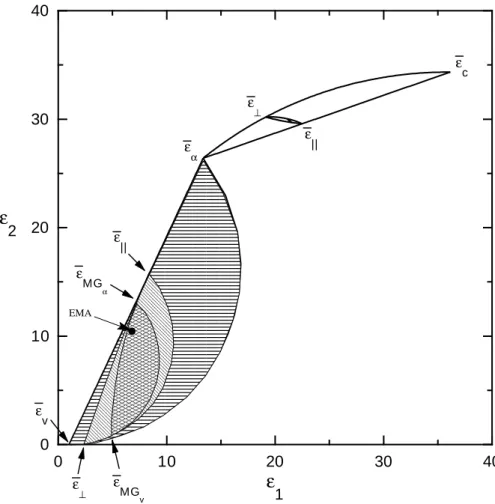
Let us consider the “amorphous silicon-void” system as shown in Fig. 1.4, and denote the volume fractions of amorphous silicon and voids asfα andfv, respectively.
The Wiener absolute bounds are defined by the screening parameter l = 0 and l = 1 for 0≥fα ≥1, i. e. a straight line between v andα (eqn. 1.46 for no screening) and a circular arc passing through v and α (eqn. 1.47 for maximum screening) enclosing the largest dashed region in Fig. 1.4, whereα andv denote the dielectric function of amorphous silicon and voids, respectively. The values=k and =⊥corresponding to the known value of fα = 1−fv can be calculated for no screening (eqn. 1.46) and for maximum screening (eqn. 1.47), respectively. k lies on the straight line between α and v and ⊥ lies on the circular arc betweenα and v.
If the compositionfa= 1−fv is fixed, the Maxwell-Garnett expression (eqn. 1.44) provides further absolute limits substituting h = α and h = v in eqn. 1.43 for 0≥ l ≥1. In this case, regardless of the shapes of the constituent regions (i. e. the value of the screening parameter l) must lie within the smaller range defined by the circular arcs passing through⊥ and k and either α orv.
For a known composition and two-dimensional (l = 1/2) or three dimensional (l = 1/3) macroscopic isotropy the smallest dashed range is defined by the so called Bergman-Milton limits through linesh =xα+ (1−x)v andh−1 =xα−1+ (1−x)v−1 for 0≥x≥1, passing through the Maxwell-Garnett pointsM Gα andM Gv and either ⊥ or k. M Gα and M Gv lie on the straight line and on the circular arc, respectively, between ⊥ and k.
If a and b are nearly equal (see the straight line and the circular arc between α andc as shown in Fig. 1.4), the allowed ranges are smaller than in the case of a very different dielectric function. If the allowed ranges are small, then the shape distribu- tions are much less important than the composition. In general, shape distribution effects are more important when the constituent dielectric functions are widely differ- ent, while composition is more important if they are similar. The relative importance of composition and shape distribution may change with wavelength.
The LL theory (h) is a poor choice for condensed-matter applications where space is filled completely and the assumption of a vacuum host is obviously artificial. The
0 10 20 30 40 0
10 20 30 40
ε⊥
ε||
εc
ε||
εMG
α
εMG
v
εα
ε⊥
εv
ε1
ε2
EMA
Figure 1.4. Limits on the allowed range offor composites with two components: α-v and α-c, where α, v and c denote the dielectric function of LP-CVD deposited amorphous silicon, voids and single-crystalline silicon evaluated at the Hg-arc UV line ofλ= 365 nm, wherec = 36.14 +i34.34 andα = 13.36 +i26.40 (taken from Ref. [Asp81]). The Wiener absolute bounds for theα-v composites at arbitrary composition and microstructure (i. e.
for screening parameters between 0 and 1 and compositions of 0≥fα ≥1, wherefα= 1−fv) are defined by the largest dashed region enclosed by the line and circular arc betweenαand v. The Maxwell-Garnett expression (eqn. 1.44) provides further absolute limits substituting h =αandh=vin eqn. 1.43 for 0≥l≥1 enclosed by the circular arcs passing through⊥ andk and eitherαorv. For a known composition and two-dimensional (l= 1/2) or three dimensional (l= 1/3) macroscopic isotropy the smallest dashed range is defined by the so called Bergman-Milton limits through linesh =xα+(1−x)v andh−1 =xα−1+(1−x)v−1 for 0≥x≥1, passing through the Maxwell-Garnett pointsM Gα andM Gv and either⊥or k. The dielectric function calculated using the Bruggeman effective-medium approximation (denoted as EMA in the figure) for the composition of fα = 0.6 is also shown in the plot (= 6.62 +i10.66). The same boundaries are also plot for theα-c system, but the allowed ranges are so small that only the region for the Bergman-Milton limits (the lines between ⊥ and k) are visible in the applied scale.
1.1 Basics of ellipsometry 13
Eip
Eis Ers Erp
Sample Polarizer
Compensator
linearly polarized
elliptically polarized linearly polarized
extinction Analyzer Detector Light source
unpolarized
Φ
Figure 1.5. Principle of a polarizer-compensator-sample-analyzer (PCSA) null ellipsometer.
choice of host dielectric function indicates that the MG models are best suited to describing configurations where the inclusions are completely surrounded by the host material. The EMA most accurately represents the aggregate structure, where an inclusion may come in contact with different materials, including material of its own type. The EMA and MG models become equivalent in the limit of dilute mixtures where the probability of an inclusion contacting another of the same type is small.
EMA is favored in the absence of any independent information about microstructure because it reduces to the appropriate MG limit in either case and treats all constituents on an equal basis.
1.1.4 Instrumentation
Null ellipsometry
The ellipsometer is basically an optical instrument that consists of two arms, whose axes lie in one plane. Fig. 1.5 shows the principle of a polarizer-compensator-sample- analyzer (PCSA) null ellipsometer. Here, the entrance optics consist of a polarizer and compensator, or quarter-wave plate, and the exit optics consist of a second polarizer, or analyzer. The polarizer-compensator combination operates as a general elliptical polarizer. To perform a measurement, the azimuth angles for the polarizer (P), com- pensator (C), and analyzer(A) have to be found such that the light flux falling on the photodetector is extinguished. Or more visually, the ellipticity of the incident beam is adjusted with the polarizer and compensator so that it is exactly canceled by reflection, i. e. the reflected beam is linearly polarized. This linearly polarized beam can then be extinguished by rotating the analyzer properly. (The null ellipsometer is the optical analogue of the AC impedance bridge.) Besides the three azimuth angles P, C, and A, the relative retardationδc of the compensator is a fourth parameter that can be adjusted in search for the null condition, if a variable-retardation compensator is used. Reading the azimuthal angles P, C, and A at the null condition, ρ can be calculated using [Azz87]
ρs = tanA tanC+ρctan(P −C)
ρctanCtan(P −C)−1, (1.49) where
ρc =Tcejδc. (1.50)
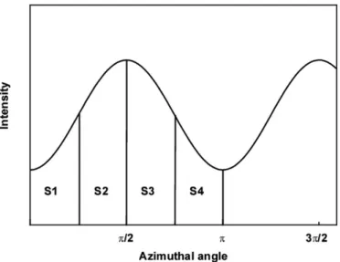
Figure 1.6. Detector signal at a rotating analyzer or a rotating polarizer ellipsometer as a function of the azimuthal angle of the rotating component.
If the compensator acts as an ideal quarter-wave retarder, then δc = −12π and Tc = 1, so in this case ρc =−j.
Photometric ellipsometry
In null ellipsometry information about the optical system under measurement is con- tained in those values of the azimuthal settings (P, C, A) of the optical elements, the relative phase retardation of the compensator (δc) and, in case of measurements on surfaces, the angle of incidence (Φ) that reduce the detected light flux to zero. Pho- tometric ellipsometry, on the other hand, is based on utilization of the variation of the detected light flux as a function of one or more of the above parameters (azimuth angle, phase retardation, or angle of incidence). The raw data from a photometric ellipsometer includes intensity signals that are obtained at prescribed conditions.
Only a few of the many photometric designs have been considered sufficiently practical. The simplest of these are the rotating-analyzer ellipsometer (RAE), and its complement, the rotating-polarizer ellipsometer (RPE). The latter configuration is used in the present study (SOPRA ES4G and SOPRA MOSS-OMA ellipsometers, see Section 2.1). In these configurations the entrance and exit optics consist of single polarizing elements. One of these is rotated mechanically, while the other is held fixed. The advantages are the simplicity and the absence of a compensator. The only wavelength-dependent element is the sample itself. A second advantage is, that the transmitted intensity has a very simple Fourier spectrum consisting of a single AC component on a DC background. The detector signal as a function of the azimuthal angle of the rotating component is shown in Fig. 1.6. Disadvantages include the requirement of either a rigorously unpolarized source for an RPE or a rigorously polarization-insensitive detector for an RAE. In addition, as with all photometric systems, the detector must be rigorously linear or has to be calibrated for non-linearity.
Finally, these configurations cannot distinguish between circularly polarized light or unpolarized light or between the right and left handedness of circularly polarized light.
In the case of a rotating-analyzer ellipsometer the detector signal takes the form
![Table 1.1. Major process steps in silicon microelectronics together with the material prop- prop-erties that can be measured by SE (after [Ire93]).](https://thumb-eu.123doks.com/thumbv2/9dokorg/1313332.105629/27.892.202.693.193.464/table-major-process-silicon-microelectronics-material-erties-measured.webp)
![Figure 1.9. Optical penetration depth (OPD) for single-crystalline silicon (c-si) [Asp85], LPCVD deposited amorphous silicon (a-Si) [Jel93] and implanted amorphous silicon (i-a-Si) [Fri92b].](https://thumb-eu.123doks.com/thumbv2/9dokorg/1313332.105629/32.892.256.634.135.425/figure-optical-penetration-crystalline-deposited-amorphous-implanted-amorphous.webp)
![Table 1.3. LPCVD reactor characteristics [Sch86]. Recently, the wafer size of 300 mm is being introduced in the microelectronics industry.](https://thumb-eu.123doks.com/thumbv2/9dokorg/1313332.105629/35.892.227.671.880.1049/table-lpcvd-reactor-characteristics-recently-introduced-microelectronics-industry.webp)