www.advopticalmat.de
ZnSnN 2 in Real Space and k-Space: Lattice Constants, Dislocation Density, and Optical Band Gap
Vegard Skiftestad Olsen,* Vetle Øversjøen, Daniela Gogova, Béla Pécz, Augustinas Galeckas, Jon Borgersen, Kjetil Karlsen, Lasse Vines, and Andrej Kuznetsov
DOI: 10.1002/adom.202100015
terms of the earth-abundancy of the mate- rial. More specifically, Zn-IV-N2 with IV = Ge, Sn or Si may have a great potential for optoelectronic applications. Indeed, the direct band gap of Zn-IV-N2 semiconductors may potentially cover the same range as that of the AlN-GaN-InN alloys,[4] and thus have the potential to be tailored to meet applica- tion-specific band gap energies.[1–3,5–7]
In particular, ZnSnN2 exhibits excel- lent properties for its use as the solar light absorber in photovoltaics and photocatalysts, but is less explored compared to that of ZnSiN2 and ZnGeN2. According to calcula- tions, the most energetically favorable struc- ture for ZnSnN2 is the orthorhombic Pna21, although the orthorhombic Pmc21 struc- ture has also been identified as a possible structure for ZnSnN2.[8] In addition to the Pna21, ZnSnN2 can also be synthesized in the hexagonal P63mc and monoclinic structures,[9–11] depending on the growth condi- tions as well as the substrate lattice-matching. Notably, the temper- ature-window for single crystalline growth of ZnSnN2 is relatively narrow. For example, Gogova et al., have reported the growth of single crystalline hexagonal layers at 350 °C by magnetron sput- tering on (0002) ZnO substrates providing a lattice mismatch of 4.2%.[12] Le et al., demonstrated epitaxially grown wurtzite films by plasma-assisted molecular beam epitaxy (PAMBE) at 450 and 550 °C, using ZnO buffer layers.[10] Thus, even though the initial demonstrations of the ZnSnN2 epitaxy have been made, there is a room for explorations.
Importantly, the exact determinations of the ZnSnN2 lattice parameters and the band gap remain unsettled. The lattice para- meter determination of ZnSnN2 obviously depends strongly on the crystal structure of the grown film. For the hexagonal P63mc structure, that is wurtzite, the parameters have often been esti- mated from the diffraction peak positions of polycrystalline films with questionable crystalline quality. In terms of the band gap energy, there is a large spread in the data obtained by theoretical calculations (1.1–2.4 eV), predicting that both the crystal struc- ture and the cation-disorder affect the band gap energy and the carrier concentration.[13–15] Experimentally, the optical gap has been found to depend on the crystal structure and carrier density in the films, which are controlled by growth parameters,[15] post- growth annealing,[16] and stoichiometry deviations.[17] Moreover, the uncertainties in the band gap energy induce a chain reaction in the analysis of the defect formation energies accounting for Fermi level dependencies. In order to reliably estimate the fun- damental band gap energy from optical absorption experiments, Semiconducting II-IV nitrides exhibit tunability of optoelectronic properties
similar to that of the group III nitrides, while comprising earth-abundant and potentially low-cost elements. However, the II-IV nitrides synthesis is imma- ture, limiting the explorations. Herein, ZnSnN2 hetero-epitaxial films grown by high-power impulse magnetron sputtering, having the quality at the level of the III-nitrides layers grown without dislocation-reducing strategies are dem- onstrated. This breakthrough, in addition to paving the way toward potential applications, enables reliable measurements of the ZnSnN2 properties in real space and k-space. In particular, for wurtzite ZnSnN2 films with total disloca- tion density of ≤ 5 × 1010 cm−2, the lattice parameters and the optical band gap (Eg) are determined with the accuracy not being accessible before for this material, e.g. Eg = 1.67 ± 0.03 eV. Thus, looking retrospectively, the authors’
data set the ZnSnN2—and perhaps more generally the II-IV nitrides—at the stage comparable to that of the beginning of the III-nitrides rising era.
Dr. V. S. Olsen, V. Øversjøen, Dr. D. Gogova, Dr. A. Galeckas, J. Borgersen, K. Karlsen, Prof. L. Vines, Prof. A. Yu. Kuznetsov Department of Physics Center for Materials Science and Nanotechnology
University of Oslo
P.O.Box 1048, Blindern, Oslo N-0316, Norway E-mail: v.s.olsen@smn.uio.no
Dr. B. Pécz
Department of Thin Film Physics
Institute of Technical Physics and Materials Science P.O. Box 49, EK MFA, Budapest 1525, Hungary Dr. G. Gogova
Central Laboratory of Solar Energy and New Energy Sources Bulgarian Academy of Science
Blvd. Tzarigradsko shosee 72, Sofia 1784, Bulgaria
The ORCID identification number(s) for the author(s) of this article can be found under https://doi.org/10.1002/adom.202100015.
1. Introduction
The II-IV nitride semiconductors attract considerable attention, governed by the tunability of the functionalities closely related to the group III nitrides,[1–3] widely used in optoelectronic applica- tions such as light emitting diodes, photo detectors, solar cells, etc.
Simplistically speaking, the substitution of the cation in III-nitride matrix with heterovalent II and IV cations is game changing in
© 2021 The Authors. Advanced Optical Materials published by Wiley-VCH GmbH. This is an open access article under the terms of the Creative Commons Attribution License, which permits use, distribution and reproduction in any medium, provided the original work is properly cited.
a high crystal quality of ZnSnN2 is imperative. Indeed composi- tional disorder, localized states, compensation, etc. modify the optical absorption onset,[18,19] increasing the uncertainty in the band gap determination. Additionally, the degenerate nature of most of the samples grown so far, attributed to native donor defects, in particular the Sn antisite (SnZn)[20,21] and/or impurities such as oxygen,[20] cause a blueshift of the band gap due to the Burstein–Moss effect.[22,23] Thus, the growth of highly crystalline, stoichiometric material, with minimal oxygen incorporation is imperative to pave the way not only for potential applications of this material, but also to determine its fundamental parameters in the real space and k-space.
Herein we report on single crystalline heteroepitaxially grown ZnSnN2 layers on (0002) ZnO, employing a high-power impulse magnetron sputtering (HiPIMS) featured by high ioni- zation of the reactive N2 gas, thus minimizing the incorpora- tion of N2 in molecular form, and relatively low base pressures in the range of 10−8 – 10−9 mbar. As a result, we present a sys- tematic analysis of the ZnSnN2 crystal quality and dislocation density affecting the optical properties of the material.
2. Results and Discussions
The ZnSnN2 epitaxial layers were grown with HiPIMS and nitrogen as reactive gas on nitrogen-implanted ZnO substrates.
The stoichiometry of the ZnSnN2 single-crystalline layers was determined by secondary electron microscopy energy dispersive X-ray spectroscopy (SEM EDS). As can be seen from Table S1,
Supporting Information, all samples (A–D) were found to be stoichiometric, at least within the accuracy of the SEM EDS, and the thickness of the epitaxial layers ranged from 487 to 623 nm.
2.1. Structural Properties
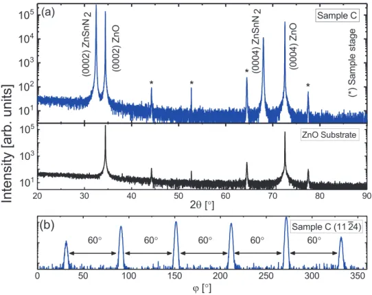
Figure 1a displays a wide locked couple X-ray diffraction (XRD) scan for sample C, and compared to the nitrogen-implanted ZnO substrate (lower panel in Figure 1a). Sample C, as well as sample A, B, and D (not shown), exhibit four dominant reflec- tions related to the thin film and substrate; i) the (0002) reflec- tion of ZnSnN2 located at 32.4°, and its higher order replica (0004) at 68.0°, and ii) the (0002) and (0004) reflections of ZnO at 34.44° and 72.52°, respectively. The remaining low intensity peaks, labeled with (*) in Figure 1a are related to the sample stage. The absence of other thin film related diffraction peaks indicates the wurtzite crystal structure of ZnSnN2 and an epi- taxial relationship between the grown layer and ZnO substrate, with growth along the <0001 > direction. As shown in the work by Quayle et al., a random mixture of Pna21 and Pmc21 poly- types stacking in the basal plane will essentially be indistin- guishable from the wurtzite structure in XRD θ/2θ scans.[14]
The epitaxial relationship to the substrate and wurtzite crystal structure of ZnSnN2 is on the other hand supported by employing phi scans. Six (1124) (Figure 1b) and six (1014) dif- fraction peaks (not shown here), all separated by 60°, confirm the sixfold symmetry of the hexagonal crystal, excluding the presence of orthorhombic phases in the layers, at least within
Figure 1. a) XRD survey scan of ZnSnN2, represented with sample C (upper panel) in comparison with the nitrogen-implanted ZnO substrate (lower panel). b) Phi scan showing the sixfold symmetry of the (1124) ZnSnN2 plane.
the detection limit of the XRD. The c-lattice constant of ZnSnN2
was calculated from the position of the (0002) reflection meas- ured by the XRD, for example, sample A c = 0.551 nm.
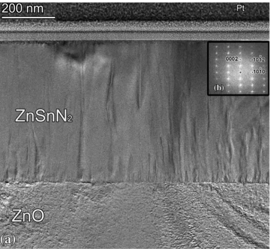
Transmission electron microscopy (TEM) analysis of the ZnSnN2 layers (Figure 2) also confirms the wurtzite crystal structure, as seen from the diffraction pattern based on the fast Fourier transform (FFT), in Figure 2b, indexed for the wurtzite crystal structure, while the orthorhombic structure could not be indexed. The lattice constants (a and c) of sample A were also found by employing FFT of the lattice k-space image; a = 0.346 ± 0.003 nm and c = 0.554 ± 0.005 nm using ZnO lattice as an internal standard. Notably, c calculated from TEM FFT and the corresponding XRD value are in agreement. Thus, combining the data in Figures 1 and 2 we conclude on high crystalline quality of epitaxial layers grown in our experi- ments, even though the threading dislocations are present.
Furthermore, from Figure 2a a strikingly flat and smooth top surface of the ZnSnN2 layer can be observed. The TEM image in Figure 2a also shows a V-shaped feature from the surface, narrowing down into the layer. Notably, the nitrogen- implanted ZnO substrate contain some residual traces of structural damage inherited from the implantation, and sub- sequent annealing to restore the crystalline quality. A high-res- olution TEM image of the ZnSnN2/ZnO inteface is shown in Figure S1, Supporting Information.
Figure 3a shows the rocking curve (ω) scan of the ZnSnN2
(0002) reflection in comparison to that of ZnO. High intensity, narrow peaks can be observed, with the corresponding FWHM values plotted in Figure 3c for the different samples illustrate excellent reliability of the growth. Notably, the rocking curve scan broadness is connected to the distribution of lattice plane tilts with respect to the film normal, and can be used as an estimation of the dislocation density. The FWHM for all sam- ples is below 0.10°, indicating relatively low density of dislo- cations. In fact, samples A and B have FWHM below 0.05°, matching that of single crystal ZnO. These values are an order of magnitude lower of what has been reported in the literature so far, for example, 0.52° for ZnSnN2 grown on ZnO buffer, employing PAMBE,[10] or 0.38° for ZnGeN2 grown on GaN buffer by MBE.[24] Notably, the use of lattice-matching sub- strates or buffer layers reduces dislocation densities as com- pared to the films grown on lattice-mismatched substrates such as, Al2O3 (0001). Figure 3b compares the rocking curves of the symmetrical (0002) and the asymmetrical (1124) reflec- tions in sample C. Evidently, the FWHM of the symmetrical reflection is smaller as compared to the asymmetrical reflec- tion. Nevertheless, the (1124) FWHM below 0.13° still indicates excellent crystalline quality. From the FWHM of the sym- metric (0002) reflection measured with rocking curve scans, the upper limit of the screw threading dislocations density Figure 2. a) Cross-sectional TEM image of sample A, showing the nitrogen-implanted ZnO substrate and the ZnSnN2 epitaxial layer. Threading disloca- tions are observed, propagating throughout the thickness of the layer. b) The diffraction pattern confirming the wurtzite structure of the epitaxial layers.
(ρs), that is with Burgers vector along the c-axis, can be esti- mated as[25]
/4.35
s 2 c2
ρ =βω (1)
where bω is the FWHM of the (0002) reflection measured with rocking curve scan, and assuming that the length of the cor- responding Burgers vector equals the c lattice parameter of ZnSnN2. Edge threading dislocations, with the density of ρe
and Burgers vector perpendicular to the c-axis, do not distort
the (000l) planes; however typically ρe > ρs in III-nitrides.[26]
For our samples ρs ranges from 1 × 10⁷ to 1.3 × 108 cm−2, see Table S2, Supporting Information. Importantly, by accounting for the edge- and mixed type threading dislocations, the total threading dislocation densities for the ZnSnN2 epitaxial layers are expected to be higher, as indicated by the higher FWHM of the (1124) rocking curve in Figure 3b.
The dislocation density of ZnSnN2 was also investigated using TEM analysis. From Figure 4a, showing the plan view surface of sample A, ≈ 60 dislocations reaching the surface are observed over Figure 3. XRD analysis of samples A-D compared to the nitrogen-implanted ZnO substrate. a) Rocking curve (ω) scan on the (0002) reflection of ZnSnN2, b) rocking curve scan on the symmetric (0002) and anti symmetric (1124) reflection of ZnSnN2 for sample C chosen as the lower quality limit example, and c) FWHM statistics from the locked couple- and rocking curve scans.
Figure 4. Dislocation density TEM analysis of sample A. a) Plan view image showing ≈60 dislocations reaching the surface. Three loops probably stemming from screw dislocations open to a shallow pit on the surface are observable. b) Bright-field image taken at two-beam conditions showing dislocations with Burgers vector (000l), that is screw-dislocations.
an area of 355 nm × 355 nm, providing the estimate for total dis- location density, ρtot, of ≈5 × 1010 cm−2. In average as measured over several regions and images, ρtot was found to vary in the range of 1 × 10¹⁰ – 5 × 1010 cm−2. Furthermore, ρs was measured by probing the dislocations with Burgers vector along the c-direc- tion, as shown in Figure 4b, resulting in ≈5 × 108 cm−2. Altogether, we confirm that in terms of the dislocation networks, ZnSnN2
exhibits the same trend as for III-nitrides: i) the films are grown with relatively high density of dislocations emerging from the sub- strate-film interface, ii) the dominant extended defects observed in this material are threading dislocations, and iii) ρe >> ρs.
2.2. Topographical Properties
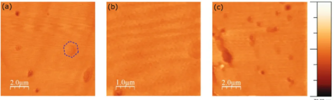
The surface of the ZnSnN2 films was evaluated employing a tuning fork scanning probe microscope (SPM), and several rep- resentative topography maps are shown in Figure 5. The single crystalline layers show remarkable flat surfaces, as also observed by the TEM. The flatness of the epitaxial layers is measured with the root-mean-square (RMS) roughness as mapped in Figure 5a–c and found to be 1.03, 0.95, and 1.51 nm, respectively, pits included. Neglecting the discrepancy due to pits results in the corresponding RMS roughness of 0.83, 0.85, and 0.61 nm, respec- tively. The smoothness of the growth surface is a known favorable feature of the HiPIMS growth, both predicted using atomistic simulations[27] and observed experimentally.[28] Interestingly, from Figure 5 there are no indications of columnar grains, typical for III-nitrides grown by sputtering,[29,30] also supported by the absence of clear grain boundaries from the TEM investigations in Figure 2a. The pits that are observable in Figure 5 have a diam- eter in the range of 0.2 –2 μm, whereas the depth of the pits are in range of 1–10 nm. Interestingly, such V-shaped surface defects (or pits), as highlighted by the hexagonal shapes in Figure 5a, are common for III-nitrides, and may occur by overgrowth caused by for example, threading dislocations[31] or inversion domains.[32]
Notably, indications of such V-shaped feature is observable in the cross-sectional TEM image in Figure 2a, and might be caused by the propagating threading dislocation underneath.
2.3. Optical Properties
The optical absorption properties of the ZnSnN2 single crys- talline layers studied by transmittance and diffuse-reflectance
methods are summarized in Figure 6. The optical band gap (Eg) values were estimated by employing the Tauc method[33]
for absorbance and the Kubelka–Munk function[34] for direct- allowed type of optical transitions, that is assuming a direct band gap of ZnSnN2. In the present work, the Eg assessment relies on identification of both the linear Tauc-segment and baseline-segment,[35] preventing a systematic underestimation of the Eg. Figure 6a shows Tauc plot representing results of the transmittance measurements, in which both the epilayer and the substrate were probed together, hence their mutual contri- butions are generally intermixed. However, this poses a minor problem for the absorption edge or Eg assessment in the case of two-layered materials with sufficiently contrasting properties, such as ZnO and ZnSnN2. Indeed, while the absorption edge at ≈3.12 eV evidently stems from the nitrogen-implanted ZnO substrate, the extensive absorption tails spreading throughout the visible spectrum are apparently of the mixed nature. None- theless, one can observe the absorption onset of the ZnSnN2 epilayers at ≈1.7 eV in the enlarged region of the spectrum (area marked in gray in Figure 6a), as presented in the inset.
The absorption onset is then confirmed by the Tauc plot rep- resenting the diffuse reflectance measurements of ZnSnN2 with the corresponding Eg estimations of 1.64–1.7 eV, shown in Figure 6b. From the data presented in Figure 6a,b and also summarized in Table S3, Supporting Information, it is clear that the optical band gaps from transmittance (EgT) and diffuse reflectance (EgR
) measurements are in good agreement for all the samples, demonstrating Eg values within the 1.64–1.7 eV range. Notably, the estimated Eg of the ZnSnN2 epitaxial layers are in excellent agreement with previous theoretical works on ZnSnN2, where local octet rule preserving ordering is present in the material.[14,36] Octet-rule-violating structures, for example, completely random distribution of cations, have been reported to decrease Eg significantly,[14,37] indicating that the Zn and Sn atoms in the epitaxial layers are arranged in such a way to locally preserve the octet rule. Note that, in general, the optical absorption onsets may deviate from the energy of the funda- mental band gap due to structural and doping effects. Indeed, the high-density structural defects are known to introduce Urbach tailing[18,19] that in effect narrows the optical band gap, whereas the opposite trend, a blue-shift of the absorption edge known as Burstein–Moss effect,[22,23] may also occur in the case of high doping caused by unintentional oxygen incorporation during growth, as well as intrinsic donor defects as the SnZn antisite. With the measured carrier concentration for sample
Figure 5. Topographical measurements at a specific position in sample C applying two magnifications (a,b) and scanning different areas using the same magnification (a,c). Notably, hexagonal shaped surface defects or pits are highlighted in panel (a) with dotted lines.
A of 3.02 × 1020 cm−3 (see Supporting Information), Burstein–
Moss effect is expected to cause a blueshift in the absorption onset compared to the fundamental band gap of the epitaxial layers, correspondingly lowering the fundamental band gap as determined in this study. In both regards, the superior crystal- linity of the stoichiometric epitaxial layers in the present study enhances the reliability of the Eg data. The spectral dependency of the optical absorption coefficient, a, presented in Figure 6c, was calculated from the transmittance measurements at room- temperature, and a step-by-step illustration of the absorption coefficient estimation can be seen in Figure S2, Supporting Information. The spectral dependency of α is naturally a mix of contributions from the epitaxial ZnSnN2 layer and the nitrogen- implanted ZnO, and the absorption of ZnO provide a reference for calibrating the absorption coefficient scale.
Finally, we note that the optical emission properties of the epitaxial ZnSnN2 layers were also addressed by employing photoluminescence (PL) and catholuminescence (CL) meas- urements (Figures S3 and S4, Supporting Information, respec- tively). Both the PL and CL quantum efficiency (yield) were found to be low, probably due to non-radiative recombination channels related to the dislocations. Notably, the high efficiency
of the non-radiative recombination channels is also known for III-nitride films and can be improved in further studies applying the dislocation-reducing strategies.
3. Conclusion
In this work, the crystal quality and its impact on optical prop- erties of ZnSnN2 epitaxial layers were investigated. The main conclusions of this work are; i) HiPIMS growth on (0002) ZnO substrates results in superior crystal quality layers with perfect epitaxial relationship to the substrate, enabling the determi- nation of the real space fundamental properties in this novel semiconductor: such as lattice parameters a = 0.346 ± 0.003 nm and c = 0.554 ± 0.005 nm. ii) Our material exhibited disloca- tion densities of 1 × 10¹⁰ – 5 × 1010 cm−2, comparable to that in III-nitrides grown without dislocation-reducing strategies. iii) The optical band gap of our material was unambiguously deter- mined to be in the range of 1.64–1.7 eV, using a combination of the transmission and diffuse reflectance approaches. Thus, we conclude that ZnSnN2 can be grown with sufficiently high crystalline quality to be considered strain free and yield reliable Figure 6. Optical characterization and band gap estimations of the ZnSnN2 epitaxial layers employing a) transmittance measurements with Tauc- analysis for direct allowed transitions and b) diffuse reflectance measurements with Kubelka–Munk analysis for direct allowed transitions. The inset in (a) shows the absorption onset of the ZnSnN2 material. c) The optical absorption coefficient for ZnSnN2 as calculated from transmittance measure- ments at room temperature. The absorption of ZnO provides a reference for calibrating the absorption coefficient scale.
determination of the fundamental properties, pawing the way for its use in optoelectronic applications.
4. Experimental Section
High-Power Impulse Magnetron Sputtering: ZnSnN2 thin films were grown using a Polyteknik Flextura cluster equipment. Two separate 3 ″ metallic targets of Zn (99.995%) and Sn (99.999%) were employed for reactive sputtering in a mixture of Ar and N2 gas. The base pressure prior to growth was below 2 × 10⁻⁸ mbar, and the deposition pressure was kept at 2 × 10⁻³ mbar, with a constant N2 flow of 20 sccm. The Ar flow was adjusted to meet the deposition pressure of 2 × 10⁻³ mbar. The substrate temperature was kept at 350 °C, and sample rotation was 10 rpm. The Zn target was placed at the HiPIMS source, and Sn target was inserted on a conventional RF magnetron sputtering source. The HiPIMS target power (Zn-target) was kept at 44 W for all depositions, whereas the RF target power (Sn-target) was varied slightly (43–49 W) around values resulting in stoichiometric films. For the HiPIMS source, the frequency was optimized to 1400 Hz.
Secondary Electron Microscopy: Compositional analysis was undertaken employing secondary electron microscopy energy dispersive X-ray spectroscopy (SEM EDS) and secondary ion mass spectrometry (SIMS).
SEM EDS measurements were conducted on a JEOL IT-300 instrument equipped with a Thermo Fisher Ultradry EDS detector. Quantification results are based on standardless phi-rho-Z analysis, with data captured using 8 kV accelerating voltage, 18% detector dead time at 108 600 cps.
Secondary Ion Mass Spectrometry: SIMS mass spectra and depth profiles were obtain using a Cameca IMS 7f microanalyzer with either 15 keV Cs+ or 10 keV O2+ as primary ions. The depth of the sputtered crater was measured by a Veeco Dektak 8 stylus profilometer. Assuming a uniform and time-independent erosion rate, the measured crater depth was used to convert sputtering time to the sample depth.
X-Ray Diffraction: XRD was utilized for structural characterization. A Bruker AXS D8 Discover system was employed. The X-ray source was Cu Ka (λ = 1.5406 Å), and a Ge (220) double bounce monochromator was implemented to filter out the Ka2 signal (λ = 1.5444 Å). The instrumental broadening of the diffraction peaks of 0.008° is included in the standard error of the values given.
Transmittance and Diffuse Reflectance: Optical absorption properties of the films were derived from the transmittance and diffuse-reflectance measurements performed at room temperature using a ThermoScientific EVO-600 UV–vis spectrophotometer.
Transmission Electron Microscopy: Transparent TEM lamella was cut by focused ion beam (FIB) in which the energy of Ga ions was reduced to 2 keV in a dual beam FEI SCIOS2 equipment. TEM was carried out in a FEI THEMIS 200 microscope equipped with an image corrector of 200 keV.
Sample Preparation: The ZnSnN2 thin films were grown on 500 μm thick single crystal (0002) ZnO commercial substrates. Prior to the growth, the O-face (0002) was box-implanted with N+ ions in order to fabricate a highly-resistive surface layer to enable subsequent reliable electrical characterization. The substrates were implanted with N ions in two steps; i) to a dose of 1 × 1014 cm−3 with an energy of 36 keV, and ii) to a dose of 2 × 1014 cm−3 with an energy of 180 keV. After implantation, the substrates were cleaned in acetone, isopropanol and di-water, dried in N2 flow and annealed in O2 atmosphere at 1150 °C for 1 h to recover structural damages caused by the implantation step, and prepare a substrate surface suited for epitaxial thin film growth. In the sputter chamber, the substrates were kept at 350 °C for 30 min before deposition to stabilize the substrate temperature, since the temperature fluctuations can strongly affect the structural properties of the material.
In between characterization steps, all films were contained in a nitrogen atmosphere to minimize the oxidation effects.
Supporting Information
Supporting Information is available from the Wiley Online Library or from the author.
Acknowledgements
This work was funded by the The Research Council of Norway (RCN) and is acknowledged for the support to the SALIENT project, project no.
239895/F20. RCN is also acknowledged for the support to the Norwegian Micro- and Nano-Fabrication Facility, NorFab, project no. 295864. The European Structural and Investment Funds is acknowledged for the support to VEKOP-2.3.3-15-2016-00002 and VEKOP-2.3.2-16-2016-00011 projects.
Conflict of Interest
The authors declare no conflict of interest.
Data Availability Statement
The data that support the findings of this study are available from the corresponding author upon reasonable request.
Keywords
band gap, dislocation density, epitaxy, high-power impulse magnetron sputtering, II-IV nitrides, lattice constants, ZnSnN2
Received: January 4, 2021 Revised: March 15, 2021 Published online:
[1] B. Gil, Group III Nitride Semiconductors Compounds: Physics and Applications, Clarendon Press, Oxford, 1998.
[2] T. R. Kuykendall, A. M. Scwartzberg, S. Aloni, Adv. Mater. 2015, 27, 5805.
[3] S. F. Chichibu, K. Kojima, A. Uedono, Y. Sato, Adv. Mater. 2017, 29, 1603644.
[4] A. Punya, T. R. Paudel, W. R. L. Lambrecht, Phys. Status Solidi C 2011, 8, 2492.
[5] A. Osinsky, V. Fuflyigin, L. D. Zhu, A. B. Goulakov, J. W. Graff, E. F. Schubert, Proc. 2000 IEEE/Cornell Conf. on High Performance Devices, IEEE, Piscataway, NJ 2000, 168.
[6] S. Kikkawa, H. Morisaka, Solid State Commun. 1999, 122, 513.
[7] P. C. Quayle, K. He, J. Shan, K. Kash, MRS Commun. 2013, 3, 135.
[8] L. Lahourcade, N. C. Coronel, K. T. Delaney, S. K. Shukla, N. A. Spaldin, H. A. Atwater, Adv. Mater. 2013, 25, 2562.
[9] N. Feldberg, B. Keen, J. D. Aldous, D. O. Scanlon, P. A. Stampe, R. J. Kennedy, R. J. Reeves, T. D. Veal, S. M. Durbin, 38th IEEE Photovoltaic Specialists Conf., IEEE, Piscataway, NJ 2012, 002524.
[10] D. D. Le, T. S. Ngo, J. H. Song, S. K. Hong, Cryst. Growth Des. 2018, 18, 1385.
[11] N. Feldberg, J. D. Aldous, P. A. Stampe, R. J. Kennedy, T. D. Veal, S. M. Durbin, J Electron. Mater. 2014, 43, 884.
[12] D. Gogova, V. S. Olsen, C. Bazioti, I. H. Lee, O. Prytz, L. Vines, A. Y. Kuznetsov, CrystEngComm 2020, 22, 6268.
[13] N. Feldberg, J. D. Aldous, W. M. Linhart, L. J. Phillips, K. Durose, P. A. Stampe, R. J. Kennedy, D. O. Scanlon, G. Vardar, R. L. Field III, T. Y. Jen, R. S. Goldman, T. D. Veal, S. M. Durbin, Appl. Phys. Lett.
2013, 103, 042109.
[14] P. C. Quayle, E. W. Blanton, A. Punya, G. T. Junno, K. He, L. Han, H. Zhao, J. Shan, W. R. L. Lambrecht, K. Kash, Phys. Rev. B 2015, 91, 205207.
[15] T. D. Veal, N. Feldberg, N. F. Quackenbush, W. M. Linhart, D. O. Scanlon, L. F. J. Piper, S. M. Durbin, Adv. Energy Mater. 2015, 5, 1501462.
[16] A. N. Fioretti, A. Stokes, M. B. Young, B. Gorman, E. S. Toberer, A. C. Tamboli, A. Azkutayev, Adv. Electron. Mater. 2017, 3, 1600544.
[17] A. N. Fioretti, A. Zakutayev, H. Moutinho, C. Melamed, J. Perkins, A. G. Norman, M. Al-Jassim, E. S. Toberer, A. C. Tamboli, J. Mater.
Chem. C 2015, 3, 11071.
[18] E. O. Kane, Solid-State Electron. 1985, 28, 3.
[19] J. K. Katahara, H. W. Hillhouse, J. Appl. Phys. 2014, 116, 173504.
[20] S. Chen, P. Narang, H. A. Atwater, L. W. Wang, Adv. Mater. 2013, 26, 311.
[21] N. Tsunoda, Y. Kumagai, A. Takahashi, F. Oba, Phys. Rev. Appl 2018, 10, 011001.
[22] E. Burstein, Phys. Rev. 1954, 93, 632.
[23] T. S. Moss, Proc. Phys. Soc. London, Sect. B 1954, 67, 775.
[24] M. B. Tellekamp, C. L. Melamed, A. G. Norman, A. Tamboli, Cryst.
Growth Des. 2020, 20, 1868.
[25] C. G. Dunn, E. F. Koch, Acta Metall. 1957, 5, 548.
[26] M. A. Moram, M. E. Vickers, Rep. Prog. Phys. 2009, 72, 036502.
[27] M. Kateb, H. Hajihoseini, J. T. Gudmundsson, S. Ingvarsson, J. Vac.
Sci. Techol. A 2019, 37, 03130.
[28] F. Lofaj, M. Kabátová, M. Klich, D. Vana, J. Dobrovodsky, Ceram.
Int. 2019, 45, 9502.
[29] H. W. Kim, N. H. Kim, Appl. Surf. Sci. 2004, 236, 192.
[30] L. Zhao, K. Yang, X. Zhang, L. Niu, H. Lv, Y. Zhang, J. Mater. Sci.:
Mater. Electron. 2018, 29, 13766.
[31] X. H. Wu, C. R. Elsass, A. Abare, M. Mack, S. Keller, P. M. Petroff, S. P. DenBaars, J. S. Speck, Appl. Phys. Lett. 1998, 72, 692.
[32] B. Pécz, Z. Makkai, M. A. de Forte-Poisson, F. Huet, R. E. Dunin-Borkowski, Appl. Phys. Lett. 2001, 78, 1529.
[33] J. Tauc, R. Grigorovici, A. Vancu, Phys. Status Solidi B 1966, 15, 627.
[34] P. Kubelka, F. Munk, Z. Tech. Phys. 1931, 12, 593.
[35] P. Makula, M. Pacia, W. Macyk, J. Phys. Chem. Lett. 2018, 9, 6814.
[36] A. Punya, W. R. L. Lambrecht, M. van Schilfgaarde, Phys. Rev. B 2011, 84, 165204.
[37] S. Lany, A. N. Fioretti, P. P. Zawadzki, L. T. Schelhas, E. S. Toberer, A. Zakutayev, A. C. Tamboli, Phys. Rev. Materials 2017, 1, 035401.