https://doi.org/10.1007/s10854-019-01906-9
Direct surface patterning of amorphous chalcogenide layers with high‑ energy H
+and He
+ion beams
S. Molnar1 · R. Bohdan1 · Gy. Nagy2 · I. Rajta2 · L. Illes3 · A. Csik2 · S. Kokenyesi1
Received: 7 June 2019 / Accepted: 18 July 2019 / Published online: 22 July 2019
© The Author(s) 2019
Abstract
As (Ge)–S (Se) based amorphous bulk chalcogenide glasses and layers have been used for surface geometrical relief record- ing by 2 MeV energy H+ and He+ ion-beams. The formation of giant (height modulation from nanometers up to microm- eters) geometrical reliefs (dots, lines), have been investigated. Efficiency of surface patterning was compared for selected compositions, type of ion beam and conductivity of substrates. Comparisons with optical and e-beam recording were made with aim to establish the details of relief formation mechanisms. The results show applicability of high-energy ion beams for in situ fabrication of planar optical elements on the surface of chalcogenide glasses (bulk samples or amorphous films).
1 Introduction
Chalcogenide glasses (ChGs), due to their high transparency in a wide spectral range (0.6–10 um) and high refractive index (n > 2), are of great interest as materials of photonics and integrated optics [1–4]. They also present interesting nonlinear optical properties, photorefractive effects, photo- induced changes of optical transmission, refractive index and even volume changes that essentially enhances functionali- ties of optical elements, fabricated from ChGs [1–8].
Applications of ChGs as materials of optical elements frequently are limited by manufacturing methods of optically and/or geometrically modulated structures in traditional fab- rication method that involves thermal evaporation of chal- cogenide glass and photolithography [9]. However there are other but less investigated and used methods of elec- tron beam or ion beam surface patterning in ChGs and local changing of optical properties (refractive index, absorption coefficient), which promise new possibilities for creating volume and surface reliefs and elements on ChGs [10–17].
Therefore, in this paper we focus on one, less investigated method: direct geometrical relief recording on the surface of As (Ge)–S (Se) based bulk chalcogenide glass plates and amorphous films by highly accelerated ion beams (H+ and He+). The aim of this work was to find reliable parameters of direct, one step recording and obtaining robust geometrical reliefs by proton- and helium ion beam irradiation, which may be used for prototyping photonic elements like micro- lenses, waveguides and diffractive elements. Comparisons with optical, laser-beam or e-beam recording allow us to make some conclusions about the mechanisms of recording process and selection of suitable glass compositions.
2 Materials and methodology
Three types of samples: bulk cleaved blocks, polished plates and thick films deposited on different transparent substrates were used in experiments for ion beam induced surface pat- terning. The selected glass compositions were: Se, As6Se94, As20Se80, As2S3, As30Ge20S50, since similar compositions were found previously as efficient materials for phase and/
or amplitude optical recording, as well as e-beam record- ing [14–16, 18]. Bulk glass samples were obtained from high-purity elemental components by standard direct syn- thesis, solidification in evacuated sealed quartz ampoules and quenching of the melt in cool water.
For ion beam patterning one type of the samples was bulk glassy Se with natural mirror-like cleaved surface. In the case of investigated As6Se94, As2S3, As30Ge20S50 bulk
* S. Molnar
molnar.ms.sandor@science.unideb.hu
1 Institute of Physics, University of Debrecen, Egyetem sq.1, Debrecen 4032, Hungary
2 Institute for Nuclear Research, Hungarian Academy of Sciences, Bem sq.18/c, Debrecen 4026, Hungary
3 Centre for Energy Research, Institute of Technical Physics and Materials Science, Hungarian Academy of Sciences, Konkoly-Thege Miklós str. 29-33, Budapest 1121, Hungary
glass samples were prepared in the form of 1–3 mm thick plates by heating up the bulk glass ingot between polished molds above the softening temperatures Tg. The third type of samples—thick amorphous films were fabricated by thermal evaporation in vacuum (10−6 Torr) onto silica glass sub- strates or silica glass covered with indium tin oxide (ITO) layer. Film thicknesses were up to 25–35 μm. The layer thickness was selected considering the stopping range of ions in chalcogenide films and eliminating the possibility of ion penetration into the glass substrate. For this reason, we made preliminary modelling of ion propagation and penetra- tion depth in our materials using SRIM (Stopping and Range of Ions in Matter) computer software package [19].
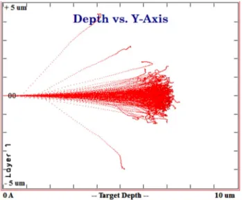
For example, according to SRIM, 2 MeV He+ in As6Se94 has a penetration depth of 7.32 µm with a longitudinal strag- gling (σ) of 0.5 µm and lateral straggling of 0.7 µm (see Fig. 1).
In the case of MeV energy light ions, the dominant energy transfer from ions to glass is the excitation and ionization of the target electrons (electronic stopping). Energy transfer through atomic collisions (nuclear stopping) is negligible in this case [20]. It is a good basis for comparison of the recording mechanism details with laser or e-beam recording, where the role of electron–hole pair excitation is essential [2, 3, 15, 21].
Ion irradiation of chalcogenide glass samples was realized by focused proton (2 MeV) and He+ (2 MeV) beams at the nuclear microprobe beamline of the Van de Graaff accelera- tor of Atomki, Hungarian Academy of Sciences. The beam spot size was 2–3 µm at the FWHM (Full Width at Half Maximum). The repetition time (frequency) of irradiation of one pixel was around 200 µs in the case of the line scan and continuous for spot recording.
The first type of scan pattern was a regular matrix of 1 pixel dots, while another scan pattern consisted of lines of various widths and spacing. The delivered ion fluences ranged between 100 and 300,000 nC/mm2, and the beam current was between 80 and 1300 pA (set according to the desired fluence). All recording experiments were done at room temperatures and in high vacuum (10−7 Torr range).
The thickness of samples as well as the surface topology of the recorded reliefs were measured by Ambios XP-1 profi- lemeter and, in more detail, by Veeco diCaliber atomic force microscope (AFM).
Fig. 1 2 MeV He+ Ion trajectories showing the penetration into As6Se94. SRIM simulation
Fig. 2 AFM profile of humps on chalcogenide glass surface. a “micro lens humps” on the surface of Se layer (ITO substrate) irradiated by He+ ions (2 MeV, I = 80pA). Dose of irradiation—0.18 nC (0.36 mJ), b “line hump” on the surface of As6Se94 layer (glass substrate), irra- diated by H+ ions. Dose of irradiation—40,000 nC/mm2, c “Grating
humps” on the surface of a-Se layer recorded by He+ ions, d Sur- face hump recorded by focused laser beam (633 nm) on surface of As20Se80 layer (Incident power = 0.5 mW, absorbed power ≈ 0.3 mW, exposure 0.54 J)
3 Experimental results
In the first cycle of experiments the samples have been irra- diated by 2 MeV protons or He+ ions in a wide range of doses. Two types of pattern geometry were recorded: spot (or matrix of spots)–“point, micro lens humps” and line (or series of parallel lines)–“line humps or gratings” (Fig. 2a–c).
The range of used dose depended on the type of the chalcogenide glass, type of ion beam and type of pattern.
On Fig. 2a one can see that a deep groove exist around the hump, which is a consequence of mass transport of chalco- genide glass from this region to the irradiated place. It is similar to the hump, recorded for comparison, by focused laser beam on the As20Se80 layer (Fig. 2d), which is a result of light-stimulated mass-transport, described for example in [22]. Besides a few experiments with optical recording by focused laser beams on the same materials for compari- son of visible effects and possible differences between ion beam and focused light recordings, comparisons were also made with data from a series of our investigations on e-beam recording [12, 15].
To eliminate the interaction between neighbor surface elements the distance between humps (or lines) were var- ied depending on chalcogenide glass composition, since the efficiency of light-induced mass transport also depends on glass composition [15, 16].
In the case of irradiation of different compositions by 2 MeV He+ ions, patterning with two different distances between linear humps have been realized (20 and 100 μm)
and 200 μm spacing for H+ ions was made. Height of the recorded linear humps was ≈ 1.5–2 times higher, if the dis- tance between humps was 100 μm compared to a 20 μm spacing on Se, As6Se94, As2S3 bulk glass. It seems that 20 μm is a very low distance between linear humps for He+ ion beam patterning on the surface of chalcogenide glasses within our experimental parameters (focusing, intensities, doses) and it may be connected to charging effects in the glass volume [23].
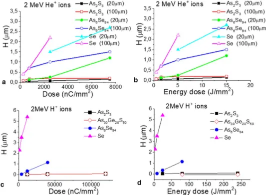
The main series of experiments on efficiency of surface relief recording on the selected compositions at similar irra- diation conditions were performed for a number of thick samples. Results are presented in Fig. 3.
4 Discussion
In our experiments the largest efficiency of ion beam (pro- ton and He+) patterning was found for amorphous selenium (Fig. 3), that basically correlates with the data on light- induced surface relief formation at equal average exposure [14, 18]. At the same time, from technology and stability points of view application of pure amorphous selenium as material for optical devices seems to be questionable, because amorphous, glassy Se is rather instable, undergoes structural transformations, crystallization. After comparison of surface relief recording efficiency at the same absorbed optical energy, we established that almost the same high optical recording parameters may be achieved on glasses
Fig. 3 Height of “linear humps”
on chalcogenide glass surface depending on the composi- tion, type of irradiating ions (H+ and He+), distance (20 μm and 100 μm) between recorded humps and dose (in nC/mm2 and J/mm2) of irradiation. a, b He+ ions, c, d H+ ions
with small, few at% addition of As, like the As6Se94. Also very good is As20Se80 which is stable, has higher softening temperature and was successfully used in our optical and e-beam recording experiments [12]. Much lower efficiency was found for ion beam recording in As2S3 and As30Ge20S50 thick plates (Fig. 3). Their advantage is the sensitivity in the green spectral region for optical recording, wider opti- cal transparency range in visible spectral region and higher softening temperatures, stability.
The rigidity of structure and the softening temperatures Tg, as well as the heat and electrical conductivities for these compositions seems to be among the first parameters, which influenced efficiency of ion beam recording.
Really, Se and As–Se compositions with small amount of As have chainy-layered floppy structure (average coordi- nation number between 2 and 2.2). The structure of As2S3 is similar but more rigid, with stronger interatomic bonds.
The increase of rigidity is characteristic for Ge-containing glasses, comprising tetrahedral structural units and increased average coordination number above 2.4. In our Se rich compositions bonding energies for Se–Se (1.9 eV), As–As (1.38 eV), As–Se (1.8 eV) bonds are also lower compared to the predominant As–S (2 eV), Ge–S (2.4 eV) and S–S (2.2 eV) bonds in As2S3 and As30Ge20S50 glasses [24].
First, the role of possible heating by ion beam and simple decrease of viscosity with temperature may be supposed, which results in faster mass-transport and increased relief heights, like it was shown in [25, 26]. If so, even a small local increase of temperature in Se sample, where the sof- tening temperature near 310 K is the smallest among our investigated compositions [27], will enhance the mass-trans- port. At the same time, the overheating of the sample to Tg temperatures should increase the reverse effect of thermal erasing [25]. These effects may be less important in high Tg glasses like As2S3 or As30Ge20Se80 even at small heating.
Since it is hard to measure the local temperature dur- ing the recording, we modelled, calculated the thermal field in the chalcogenide layer induced by ion beam and light irradiation.
In the case of the He+ ion beam irradiation of Se layer (cross section of resulting hump shown on Fig. 2a) at beam current of 80 pA and 2 MeV ion energy the absorbed ion beam power is 0.16 mW. The spot size (diameter) was ≈ 2.5 μm and stopping depth for the ions was ≈ 8 μm.
In the case of laser beam irradiation of As20Se80 layer (Fig. 2d) the power of the focused light beam was ≈ 0.5 mW.
Close to 60% of light energy (at λ = 633 nm) was absorbed (and ≈ 17% of light power was reflected, ≈ 20% of light power was transmitted). Therefore, approximately 0.3 mW of the power was absorbed. The diameter of the laser light spot was close to 2–3 μm (Fig. 2d).
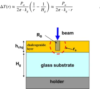
For r >rs ≈ 10 μm, (rs is the minimal size of thermal field, where the spherical symmetry model is applicable, see Fig. 4)
the thermal field in the chalcogenide layer may have a (semi) sphere symmetry, if the thickness Hg of the glass substrate (1 mm) is much larger than the ChG layer thickness, and rs is larger than the penetration depth and diameter of the ion or light beam. This approximation can apply to the region from rs to the metal sample holder (its temperature equals to room temperature), which has much higher thermal conductivity as compared to the glasses.
In a spherical coordinate system the dependence of the tem- perature on the radius r (r > rs) can be approximated by the differential equation:
where kg (T) is the thermal conductivity of the glass, which can depend on the temperature (T), Pa is the absorbed power of the laser light.
To simplify the calculations we neglect the temperature dependence of thermal conductivity of glasses (substrate or chalcogenide) and use one coefficient of thermal conductivity for the system.
For the calculation, we can use the thermal conductivity of glass substrate: 0.8–1 W·m−1·K−1 or we can correct this cal- culation by using the thermal conductivity of the chalcogenide glass layer (~ 0.7 W·m−1·K−1 for Se and ~ 0.8 W· m−1 K−1 for As40Se60 [28, 29]. The boundary conditions of temperature field can be expressed as: T → TM at R → Hg, where TM—tem- perature of the metal holder (≈ room temperature).
The solution of the differential Eq. (1) gives an increase of temperature ΔT (ΔT = T(r) − Troom) as a function of r (at rs < r≪Hg):
(1) Pa ≈ −2𝜋⋅kg(T)⋅r2⋅dT∕dr
(2) ΔT(r) ≈ Pa
2𝜋⋅kg (1
r − 1 Hg
)
≈ Pa 2𝜋⋅kg⋅r
Fig. 4 Schematic representation of spot irradiation (ion or light) of a chalcogenide layer. hchg, chalcogenide layer thickness (10 μm); Hg, glass substrate thickness (1 mm); RB, range of beam penetration (ion or light); rs, radius of quasi spherical heat field distribution; Holder, metal plate
For r = 10 μm: in the case of Se layer (2 MeV He+ ion beam, I = 80 pA, power 0.16 mW) ΔT ≈ 2.5 K and in the case of As20Se80 layer (0.3 mW, 633 nm laser beam) ΔT ≈ 5 K. The lower thermal conductivity of chalcogenide glass in com- parison with thermal conductivity of the glass substrate can increase the heat effect approximately in 1.5 times. So from our calculations for the given experimental conditions (beam intensity, radius) no significant temperature rise in the sam- ple should occur, i.e. it can be neglected or have small influ- ence in compositions with Tg higher than in a-Se.
The rise of temperature ΔT should be higher at r < 10 μm.
It depends on the intensity distribution in the beam (ions or light) and their focusing. At r ≪ 10 μm the temperature can be close to Tg of the chalcogenide glass or higher. It is more likely to occur in Se, as it was described in [30].
The increase of temperature (to T⪅ Tg) increases the light induced mass transport efficiency [26] and decreases it at temperatures above Tg [25]. So, if the light induced mass transport and ion beam patterning have similar nature then the ion beam patterning can be more effective in case of Se layer than in As20Se80 or As2S3 layers at similar parameters of irradiation just due to the heating effects. (Figure 3).
Although, very good beam focusing can decrease ion beam patterning efficiency if heating is strong, the local tem- perature is larger than Tg of the chalcogenide glass, because the hump pattern will be erased by the heat, and even dip may be produced [30]. At extreme cases even evaporation, ablation, hole formation can be produced.
Some differences between patterning process by He+ and H+ beams, at the same energy exposure may depend on their different beam parameters: current, spot form, focusing (Gaussian beam intensity distribution), penetration depth, linear energy transfer. In our case, the efficiency of ion beam patterning of ChGs (Fig. 3) shows that He+ ion beam pat- terning of chalcogenide glasses is more effective than H+ ion beam patterning. This difference ranges from ~ 2 times in case of Se to ~ 30 times in the case of As2S3 (Fig. 3). For Se glass, the 2 MeV He+ ion penetration depth is around 7–8 μm and for the same energy H+ ion it is 41–42 μm.
Linear energy transfer (deposited energy per unit depth) for He+ ions was 5–10 times larger compared to H+ ions accord- ing to SRIM simulations in our materials. The linear energy transfer in Se for He+ ions is 236 keV/μm and 31 keV/μm for H+ ions. Similar results can be obtained for the other inves- tigated compositions too. This higher deposited energy per unit depth may cause greater changes in the material, which could explain the higher patterning efficiency with He+ ions, especially in As–Se compositions compared to sulphides, because of the former’s lower viscosity, also connected with structure [31].
Further challenging question related to the record- ing mechanism in the investigated glasses may be con- nected with pore, bubble formation, especially at elevated
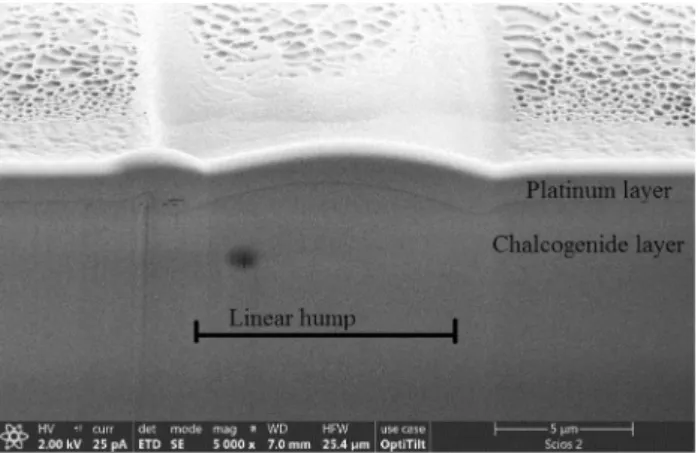
temperatures. The last were excluded by the selection of exposition conditions and supported by direct FIB and SEM observations of hump and layer cross-sections in composi- tions like As20Se80, where no phase-separated regions were found (see Fig. 5).
Local EDX measurements on As20Se80 layer cross-sec- tions gave no measurable composition changes between the irradiated and non-irradiated area. There may be still some small, near 1% local expansion–contraction even at short ion beam irradiation due to the local amorphous structure transformations towards more disordered state, like it was observed in Se and many amorphous chalcogenide layers [3, 6, 32] under light irradiation. At our experimental conditions (layer thickness, interaction volume) it can give us maximum a few hundred nanometers of surface relief height, which is much smaller than observed. Still it can be a component of any (light, beam) recording in amorphous chalcogenide lay- ers connected with unavoidable structural transformations, bond breaking-rearrangement within amorphous phase.
In our cases of ion beam recording the charging of irradi- ated spots and appearance of electrical, polarization forces at the edges of Gaussian beam intensity distribution also may have essential influence, since the volume diffusion of charged glass components, small clusters depends on the built-in electric field, as it was described in [12, 15, 21].
This effect should be and was higher in our layer samples deposited on dielectric substrates.
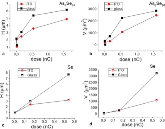
Therefore, the influence of substrate conductivity on hump height and volume also have been investigated. We compared height and volume of the hump on the surface of Se and As6Se94 layers irradiated by 2 MeV of He+ ions.
In both cases the influence of substrate conductivity on height and volume of the produced hump were observed.
For chalcogenide glasses deposited on the surface of vitre- ous glass without ITO layer the humps had larger height and volume (Fig. 6). This effect can be explained by the
Fig. 5 FIB/SEM cross-section image of As20Se80 surface irradiated by 2 MeV He+ ions
role of Coulomb force repulsion –attraction effect in irra- diated and surrounding surface areas, in the surface defor- mation process and volume expansion.
Penetrating the chalcogenide glass layer, the ions cre- ate an electric charge around their stopping region. The electric field magnitude (E) around the charged zone can be evaluated, but the magnitude of the electric field must be limited by avalanche multiplication threshold in ChG.
In case of amorphous Se it is 7*107 V/m [33, 34]. Here, the avalanche multiplication in ChG may be stimulated by ion beam. Therefore, we think that the extra patterning of layers may happen at the electric field magnitude higher than ~ 7*107 V/m, which is possible at high exposures because the high electrical resistivity of ChG (for exam- ple ρ selenium ≈ 1014 Ω∙m [35]) does not allow to reduce the charge around the beam stopping zone without ava- lanche process. This built-in electric field can also stress the chalcogenide glass and cause additional surface defor- mation. This effect is supported by that with an insulator substrate surface humps are higher than in samples with the conductive ITO covered substrate (Fig. 6), where the ITO layer grounds the charges. Besides the influence on charge related processes, the interface can influence the heat transfer and adhesion between chalcogenide and sub- strate glasses. In our approximation of the thermal model we neglect these, because the adhesion on the boundary of chalcogenide and substrate is usually good, the transition layers are thin and therefore the thermal contact must be good between the two glasses.
Further comparisons may be made with efficiency of opti- cal recording, but here again additional effects like optical fields [36], influence of polarized illumination or just the experimental conditions of holographic recording with polarized laser beams [7, 8] introduce additional variables which make difficult calculated comparisons. For example, we also compared efficiency of micro lens hump pattern- ing by He+ ion beam and e-beam beam on amorphous sele- nium. In the case of He+ (2 MeV) the efficiency is ~ 6 nm/
μJ (Fig. 3a). For electron beam (30 keV and current 5 nA, total energy per hump 750 μJ and height ~ 1.1 μm [37]) the maximum of efficiency (efficiency depends on scanning frequency) is ~ 1.5 nm/μJ. That shows 4 times higher effi- ciency of ion beam patterning in comparison with efficiency of electron beam recording. This difference can be caused by charge multiplication and also by larger penetration depth of ions than electrons to ChG.
Comparisons of our present data with light- and e-beam induced giant relief formation effects support the most gen- eral conclusion about the basic similarities of relief for- mation at ion or photon, electron irradiations, due to the stimulated structural transformations and mass-transport processes. These start with electron–hole excitation, charged defect creation, local structural changes and continues in directed shift of charged elements (chalcogens, pnictides, structural chain fragments) due to the gradients of chemi- cal potentials, electric fields, capillary effects, like it was described in [21]. At the same time, one difference is the absence of possible light polarization effects on recording,
Fig. 6 He+ (2 MeV) ion-beam patterning efficiency (height and volume of “micro lens humps”
on substrate conductivity (conductive or not conductive):
a, b As6Se94 (layer thickness 25 μm); c, d Se (layer thickness 26 μm)
which are well separated in laser-recording processes on chalcogenide glasses. Another difference is the increased efficiency of excitation by ions in a deep interaction volume, which makes the ion beam prototyping favorable in thick layers or bulk glass elements.
5 Conclusions
2 MeV energy H+ and He+ ion-beams have been used for direct, one step recording surface geometrical reliefs in As (Ge)–S (Se) based bulk chalcogenide glasses and thick amorphous layers. Five typical selected chalcogenide glass compositions: Se, As6Se94, As20Se80, As2S3 and As30Ge20S50 were compared based on the efficiency of recording (the height of the geometrical surface relief). The investigation showed that this method of in situ surface patterning (height modulation from nanometers up to micrometers) could be used for fabrication of geometrical reliefs and elements (dots of lens matrix, lines of diffractive elements, etc.) on the sur- face of bulk chalcogenide glasses and amorphous layers.
The highest efficiency of ion beam patterning was shown for amorphous selenium. Close to this, good parameters were demonstrated on As6Se94, which is stable, does not crystallize in contrast to Se.
Coulomb forces due to the absorbed ions and generated charge gradients, temperature gradients, mass transport in these gradient fields as well as simple local disordering, structural transformation of glass network within amor- phous phase play a common role in surface patterning, while the ion beam patterning seems to be energetically the most efficient.
Acknowledgements Open access funding provided by University of Debrecen (DE). The authors acknowledge the financial support of the GINOP-2.3.2-15-2016-00041 project.
Open Access This article is distributed under the terms of the Crea- tive Commons Attribution 4.0 International License (http://creat iveco mmons .org/licen ses/by/4.0/), which permits unrestricted use, distribu- tion, and reproduction in any medium, provided you give appropriate credit to the original author(s) and the source, provide a link to the Creative Commons license, and indicate if changes were made.
References
1. K. Tanaka, K. Shimakawa, Amorphous Chalcogenide Semicon- ductors and Related Materials (Springer, New York, 2011) 2. J.-L. Adam, X. Zhang, Chalcogenide Glasses. Preparation, Prop-
erties and Applications (Woodhead Publishing, Sawston, 2013)
3. S. Kugler, K. Shimakawa, Amorphous Semiconductors (Cam- bridge U. Press, Cambridge, 2015)
4. R. Wang, Amorphous Chalcogenides, Advances and Applications (Pan Stanford Publishing, CRC Press, Boca Raton, 2013) 5. A. Zakery, S.R. Elliott, Optical Nonlinearities in Chalcogenide
Glasses and their Applications (Springer, New York, 2007) 6. A. Kikineshi, Opt. Mem Neural Netw. 4(3), 177–183 (1995) 7. U. Gethers, J. Teteris, Opt. Mater. 32(8), 807–810 (2010) 8. M.L. Trunov, P.M. Lytvyn, S.N. Yannopoulos, I.A. Szabo, S.
Kokenyesi, Appl. Phys. Lett. 99, 051906 (2011)
9. A. Kovalskiy, J. Cech, C.L. Tan, W.R. Heffner, E. Miller, C.M.
Waits, M. Dubey, W. Churaman, M. Vlcek, H. Jain, Adv. Resist Mater. Process. Technol. XXVI, 72734A (2009). https ://doi.
org/10.1117/12.81164 6
10. G.B. Hoffman, W.-C. Liu, W. Zhou, R. Sooryakumar, P. Bool- chand, R.M. Renao, J. Vac. Sci. Technol., B 26, 2478–2483 (2008) 11. I. Ivan, S. Szegedi, L. Daroczi, I.A. Szabo, S. Kokenyesi, Nucl.
Instrum. Methods Phys. Res. B 229, 240–245 (2005)
12. C. Cserhati, S. Charnovych, P.M. Lytvyn, M.L. Trunov, D.L.
Beke, Yu. Kaganovskii, S. Kokenyesi, Mater. Lett. 85, 113–116 (2012)
13. Q. An, C. Cheng, S.K. Vanga, A.A. Bettiol, F. Chen, J. Lightwave Technol. 32(22), 3763 (2014)
14. S. Molnar, R. Bohdan, I. Csarnovics, I. Burunkova, S. Kokenyesi, Proc. SPIE 9359, 935908 (2015)
15. M.L. Trunov, C. Cserháti, P.M. Lytvyn, Yu. Kaganovskii, J. Phys.
D 46(24), 245303 (2013)
16. I. Csarnovics, C. Cserhati, S. Kokenyesi, T. Nichol, M. Veres, JOAM 18(9–10), 793–797 (2016)
17. T. Nichol, M.R. Latif, M.S. Ailavajhala, D.A. Tenne, Y. Gonzalez- Velo, H. Barnaby, M.N. Kozicki, M. Mitkova, IEEE Trans. Nucl.
Sci. 61(6), 2855–2861 (2014)
18. R. Bohdan, S. Molnar, S. Kokenyesi, Phys. Status Solidi A 212, 2186–2190 (2015)
19. J.F. Ziegler, M.D. Ziegler, J.P. Biersack, Nucl. Instr. Method Phys.
Res. B 268(11–12), 1818–1823 (2010)
20. M.B.H. Breese, D.N. Jamieson, P.J.C. King, Materials Analysis Using a Nuclear Microprobe (Wiley, Hoboken, 1996)
21. Yu. Kaganovskii, M.L. Trunov, D.L. Beke, S. Kökényesi, Mater.
Lett. 66(1), 159–161 (2012)
22. Yu. Kaganovskii, D.L. Beke, S. Charnovych, S. Kökényesi, M.L.
Trunov, J. Appl. Phys. 110(6), 063502 (2011)
23. V. Bilanych, V. Komanicky, M. Kozejova, A. Feher, A. Koval- cikova, F. Lofaj, V. Kuzma, V. Rizak, Thin Solid Films 616, 86–94 (2016)
24. L. Tichy, H. Ticha, J. Non Cryst. Solids 189(1–2), 141–146 (1995) 25. S. Molnar, R. Bohdan, V. Takats, Y. Kaganovskii, S. Kokenyesi,
Phys. Status Solidi A 215, 1800589 (2018)
26. M.L. Trunov, P.M. Lytvyn, J. Non-Cryst. Solids 493, 86–93 (2018)
27. Z. Borisova, Glassy Semiconductors (Plenum Press, New York, 1981)
28. G.B. Abdullaev, S.I. Mekhtieva, D.S.H. Abdinov, G.M. Aliev, S.G. Alieva, Phys. Status Solidi 13, 315 (1966)
29. B.T. Kolomiec, P. Shilo, L. Štourač, C. Musil, F. Štrba, Czecho- slov. J. Phys. B 21(6), 657–661 (1971)
30. R. Bohdan, S. Molnar, I. Csarnovics, M. Veres, A. Csik, S. Koke- nyesi, J. Non-Cryst. Solids 408, 57–61 (2015)
31. A.S. Tverjanovich, Glass Phys. Chem 29(6), 532–536 (2003)
32. D.M. Bercha, A.A. Kikineshi, M.I. Marjan, Ukr. Phys. J. 26(6), 978–981 (1981). (in Russian)
33. A. Reznik, S.D. Baranovskii, O. Rubel, K. Jandieri, S.O. Kasap, Y. Ohkawa, M. Kubota, K. Tanioka, J.A. Rowlands, J. Non-Cryst.
Solids 354(19–25), 2691–2696 (2008)
34. O. Bubon, G. DeCrescenzo, J.A. Rowlands, A. Reznik, J. Non- Cryst. Solids 358(17), 2431–2433 (2012)
35. N. Toyosawa, K. Tanaka, Phys. Rev. B 12, 56 (1997)
36. A. Saliminia, T. Galstian, A. Villeneuve, Phys. Rev. Lett. 85, 4112–4115 (2000)
37. C. Cserhati, I. Csarnovics, L. Harasztosi, M.L. Trunov, S. Koke- nyesi, J. Mater. Sci. 28(10), 7024–7028 (2017)
Publisher’s Note Springer Nature remains neutral with regard to jurisdictional claims in published maps and institutional affiliations.