Journal of Non-Crystalline Solids 553 (2021) 120491
Available online 6 December 2020
0022-3093/© 2020 The Authors. Published by Elsevier B.V. This is an open access article under the CC BY-NC-ND license
(http://creativecommons.org/licenses/by-nc-nd/4.0/).
Surface plasmon enhanced light-induced changes in Ge-Se amorphous chalcogenide – gold nanostructures
Istv ´ an Csarnovics
a,*, Mikl ´ os Veres
b, Petr Nemec
c, S ´ andor Moln ´ ar
a, S ´ andor K ok ¨ ´ enyesi
daDepartment of Experimental Physics, University of Debrecen, Bem sq 18/a, 4026, Hungary
bWigner Research Centre for Physics, Konkoly-Thege Mikl´os st. 29-33, 1121, Hungary
cDepartment of Graphic Arts and Photophysics, Faculty of Chemical Technology, University of Pardubice, Studentska 573, 53210, Czech Republic
dDepartment of Electrical Engineering, University of Debrecen, Bem sq 18/a, 4026, Hungary
A R T I C L E I N F O Keywords:
Amorphous chalcogenides Light-induced effects Gold nanoparticles Surface patterns
Localized surface plasmon resonance Surface-enhanced Raman scattering
A B S T R A C T
In this paper, the plasmon field enhanced light-induced changes are investigated in the amorphous Ge24Se76 layer incorporating Au nanoparticles. The presence of gold nanoobjects in amorphous chalcogenide/gold het- erostructure influences the optical and structural properties, as well as volume changes of the material. It also enhances the Raman signal of the structure through surface enhancement, which allows clearer and better investigation of the glass structure and understanding of the mechanisms of surface plasmon stimulated trans- formations. In addition, it also enhances the recording of the optical grating pattern into the layer.
1. Introduction
Light- or electron-beam-induced processes like optical bleaching and darkening, thickness changes (contraction or expansion), structural modifications (bond breaking and reorganization), atomic rearrange- ments and lateral mass transfer occur in chalcogenide layers during irradiation with close to band-gap photon energies [1-7]. These phe- nomena involve the interaction of light with the chalcogenide structure and strongly depend on the properties of the illumination. Therefore, the control of light intensity distribution and its amplification should have a crucial role in the character of structural transformations in chalco- genide glasses. In this regard, the amplification of the electromagnetic field of photons by localized plasmons of metallic nanoparticles, reaching a few orders of magnitude, is of particular interest.
During illumination, the electric field of the incident light induces electron oscillations in metals. Under certain conditions, this results in resonant coupling of the electromagnetic field to the electron oscilla- tions, called plasmons. This way surface plasmons may be generated on the surface of gold/silver/copper thin films at certain irradiation con- ditions, while localized surface plasmon resonance (LSPR) may occur in nanostructured metallic objects [8,9]. These plasmon resonances have many applications like localized surface plasmon resonance spectros- copy, surface-enhanced Raman scattering (SERS), etc. The plasmon wavelength of gold nanoparticles (GNP) can be controlled during the
preparation by changing their size, shape, and distances between them [10,11].
Nanosized spherical GNP show LSPR in the visible and near-infrared region of the spectrum where amorphous chalcogenides are most sen- sitive to light irradiation and have respective optical bandgap energies.
The plasmon field of GNPs was found to affect the light-induced modi- fications in amorphous chalcogenides [12-14]. It was shown how the surface plasmon modes of an island type thin gold layers and nano- structures influence the chalcogenides film’s parameters [15-22], and that the plasmon field of gold nanostructures is suitable for sensing applications in the plasmonic-chalcogenide system [23-30].
While earlier studies were focusing on the As-Se system, the aim of this paper is to investigate the influence of LSPR created with gold nanoparticles on light-induced changes in the Ge24Se76 chalcogenide.
Ge24Se76 was found to be environmentally more friendly than other chalcogenides, biocompatible and usable for the development of optical sensors. Experiments on light-induced optical, structural and volume changes have been performed on a composite structure, consisting of the chalcogenide layer and embedded gold nanoparticles. The obtained data were compared with results obtained on a pure chalcogenide layer.
2. Experimental details
The plasmonic nanoparticles being most appropriate for the
* Corresponding author: Istvan Csarnovcs, 18/a Bem sq, Debrecen, Hungary, 4026.
E-mail address: csarnovics.istvan@science.unideb.hu (I. Csarnovics).
Contents lists available at ScienceDirect
Journal of Non-Crystalline Solids
journal homepage: www.elsevier.com/locate/jnoncrysol
https://doi.org/10.1016/j.jnoncrysol.2020.120491
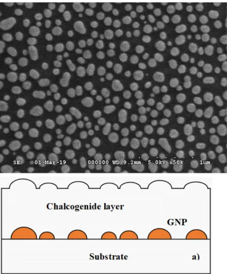
experiments have been selected after taking into account that the Ge24Se76 structure is most sensitive in the green region of the spectrum, as it was shown in our previous papers [31,32]. Depending on their size and inter particular distance the LSPR wavelength of GNPs is in the green-red spectral region. The schematic diagram of the created struc- tures is shown in Figure 1.a. For nanoparticle preparation, a 12 nm thick gold film was evaporated on a glass substrate. Particle formation occurred during annealing of the deposited layer at 550◦C for 4 hours.
The obtained sample was examined by scanning electron microscopy (SEM) (Hitachi S-4300) in different places and using several magnifi- cations, and the SEM images were used to establish the nanoparticle size and the inter particular distance (Figure 1.b). The images were analyzed with the National Instruments Vision Assistant software package and a custom Matlab code. The size of the nanoparticles and the inter partic- ular distance was found to be about 75 nm and 25 nm, respectively, and the uncertainty of the measurement was 5 %. The plasmon resonance wavelength was determined with an optical spectrophotometer (Shi- madzu UV3600) in air, and the LSPR wavelength was found to be close to 550 nm.
The chalcogenide layer was deposited on clean and GNP coated glass substrates. The Ge20Se80 glass used as a precursor material for amor- phous chalcogenide layer deposition was synthesized from high purity elements in silica ampoules by the melt-quenching process. Ge24Se76
thin films were prepared on a blank and coated with the above- mentioned gold nanostructures silica glass plates from this bulk glass by pulsed laser deposition (PLD) technique. The deposition was done in a vacuum chamber (pressure <4 ×10⁻⁴ Pa) with a KrF excimer laser (20
Hz repetition rate, 300±3 mJ per pulse, 30 ns pulse duration, λ =248 nm). The substrates were placed at 5 cm distance from the surface of the Ge20Se80 chalcogenide glass target. The laser energy on the target was
~2.6 J/cm2. The thickness of the layers was controlled by the duration of the calibrated deposition process and was about 500 nm. The composition of the created layers was established by Energy Dispersive X-Ray Spectroscopy (EDS) using the SEM system.
Light-induced changes were investigated on the as-deposited sam- ples. Their optical transmission was established by a Shimadzu UV-3600 spectrophotometer. The transmittance spectrum was recorded before and after the laser illumination. The time dependence of the trans- mittance during irradiation was investigated in situ with a power meter setup. The heterostructure sample was irradiated at normal conditions in the air with a laser diode (operating wavelength is 533 nm and power – 34 mW/cm2). The as-deposited layer was illuminated through a 2 mm hole with the same light source. Optical parameters (absorption coeffi- cient, refractive index, and optical bandgap) of the investigated samples were determined from the obtained transmittance data by using the Swanepoel method [33]. The holographic gratings were recorded for 4 hours by the well-known configuration, consisting of 2 vertically-polarized and 1 horizontally-polarized additional laser beam of the same intensity [34,35]. As a result, gratings with a 6 μm period were obtained.
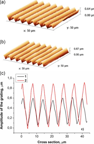
The created surface structures were studied by atomic force micro- scope (AFM) in tapping mode. The obtained data were used to establish the average height of the grating, for which the samples were examined in 7-12 different points. The error of the measurements was about 2-3%.
Figure 1.a) Schematic diagram of the created structures with gold nanoparticles and chalcogenide layer. b) SEM picture of the created GNPs.
The structural changes due to irradiation were measured by Raman spectroscopy using a Renishaw 1000B and Horiba Labram micro-Raman spectrometers with a 785 nm laser diode as the excitation source and a long working distance microscope objective of 50x magnification (NA=0.50). The intensity of the laser was reduced to <1mW at the sample surface in order to avoid damages and light-induced trans- formation of the samples. Spectra were baseline-corrected with the built-in algorithm of the Raman spectrometer software, then normalized and fitted with a set of Gaussians in order to obtain the Raman peak parameters. The error of the fitting and calculation of the investigated peaks and their parameters was about 0.5-1 %.
3. Results and discussion
The pure and GNP containing chalcogenide films have slightly different optical transmittance (Figure 2.a). While the characteristic interference pattern can be seen in both spectra, the pure layer has higher transmittance levels. As a comparison with the spectrum of the glass plate with GNPs (and without chalcogenide layer) shows, this can be attributed to the presence of the metallic nanoparticles. However, their optical properties do not affect the absorption edge which appears in the same wavelength region for both chalcogenide samples.
The light-induced red-shift of the transmission edge (photo-dark- ening, PD) was observed in As-Se(S) materials (both in pure chalco- genide film and in heterostructures with GNP) earlier, where the rate of the change was faster and more pronounced in the samples incorpo- rating metallic nanoparticles [13,36]. A similar PD process was found to take place in our Ge24Se76 chalcogenide layer [37], where the decrease of the transmittance reached a minimum after a certain time of irradi- ation. This effect has been observed in our pure chalcogenide structure as well (see Fig. 2.b). In contrast, the heterostructure with GNPs behaves differently. After a very short and fast PD stage the transmittance changes in the opposite way: the light-induced blue shift of the trans- mission edge, photo-bleaching (PB) occurs, which is unusual for Ge-Se chalcogenide layers (Figure 2.b).
The observed PD and PB effects in the two samples could be related to the changes in the layer thickness. For the heterostructure, it was found to be 7 nm (+/- 3 nm) smaller after the irradiation, while an in- crease of 15 nm (+/- 3 nm) was observed for the pure chalcogenide layer. Since the GNPs are the only difference between the two samples, this finding can be attributed to their presence. Previous experiments [14] aimed at the determination of the direction and value of the light-induced volume and thickness changes showed that they depend on the irradiation power. This suggests that it is the local increase of the irradiation intensity in the heterostructure by the plasmon field of GNPs that causes thinning of the layer.
Some optical parameters of these rather thin layers can be estimated
from the measured transmittance data using the Swanepoel method: the refractive index of the pure amorphous chalcogenide layer was found to be 2.45 near 700 nm, while it is 2.66 for the heterostructure with GNP, and increases by ~ 0.05 after irradiation. Besides that, the optical bandgaps for these samples are estimated to be near 2.02 eV. and 1.96 eV, while the absorption coefficients calculated at the irradiation wavelength (533 nm) are 3.45*104 cm−1 and 3.98*104 cm−1, respectively.
The above results indicate that the plasmon field of the metallic nanoparticles strongly influences the photo-induced structural changes in the Ge24Se76 structure. To see how this interaction affects local glass structures, Raman spectra of the as-deposited and illuminated layers were measured (Figure 3). The Raman spectrum of the Ge24Se76 layer contains the following vibrational modes: a band at 194 cm−1 corre- sponding to the vibrations of corner-sharing (CS) tetrahedra, a sideband close to 210 cm−1 related to the edge-sharing (ES) tetrahedra, and a broadband near 250 cm−1 belonging to selenium-selenium (SE) bonds of the Se polymeric chain [38-41]. This peak position is stiffened and softened due to interlayer coupling [42,43]. There is a significant enhancement of the intensity of the Ge-Se and Se-Se Raman contribution in the heterostructure (by 2.5 times, see Figure 3.a), which could arise from surface-enhanced Raman scattering involving the gold nano- particles [44]. It has been shown earlier the interaction of the incident and/or scattered light with surface plasmon oscillations in close vicinity of the GNP surface will result in a significant increase of the Raman signal of the chalcogenide layer [45,46].
The Raman peak parameters are shown in Table 1, where the CS/ES, CS/SE and ES/SE area ratios are provided for Ge24Se76 and Ge24Se76/ GNP samples in as-deposited and irradiated states. It can be seen that during laser irradiation of the samples, the intensity of the peaks con- nected to homopolar (Se-Se) bonds reduces (both CS/SE and ES/SE ra- tios increase after the irradiation), indicating homopolar bond breaking and heteropolar Ge-Se bond formation. The latter (an increase of CS and ES ratios) agrees well with the observations presented in [3].
The experimental data described above show that the pure Ge24Se76
sample exhibits a PD, while the heterostructure with GNPs – a fast PD and a slow PB process during illumination. This is accompanied by the rise of the CS/SE and ES/SE ratios in the corresponding Raman spectra, indicating homopolar bond breaking and heteropolar bond formation.
In addition, the CS/ES ratio decreases (see Table 1), indicating the reorganization of corner-sharing units into edge-shared ones. Since an ES configuration requires less Se atoms than the CS one, this means that a large number of free Se atoms is formed in the structure during illumination.
The PD process in the pure Ge24Se76 sample presumably has similar origin than in the As-based chalcogenides, where it is described by bond breaking, bond switching and corresponding atomic motion in the
Figure 2. a) Optical transmission spectra of the pure [1] and GNP containing [2] chalcogenide layer and the GNP sample without the glass [3]. b) Change of the transmittance with time at the illumination wavelength of 533 nm in pure [1] and GNP containing [2] Ge24Se76 layer.
structure [46]. As we showed earlier, the PB process could be connected with the change of the layer thickness. The laser illumination influences not only the chalcogenide layer but also enhances the plasmon field of the GNPs, resulting in increased mobility of the atoms and decreased viscosity in the material. However, according to an earlier developed theory [5, 47], the raise of the laser intensity to a definite threshold causes the reduction of the lateral mass transport and changes its di- rection. So, it is possible to detect a transition from bump, valley to
hillock formation in the irradiated place that is connected with the bulk (volume) diffusion process and its linear dependence on the power of photons.
In order to understand better the effect of the GNPs plasmon field on the light-induced modifications in the Ge-Se chalcogenide layer, the holographic recording has been performed on both samples with the same parameters. As a result, good quality surface relief gratings were obtained in both cases (see the AFM data in Figure 4). It can be recog- nized that the amplitude of the grating is 320 nm for the pure chalco- genide sample and 440 nm for the heterostructure, which means that the volume change in the two structures is 64% and 88% of the initial film thickness, respectively. Previously it was shown, that Se atoms has an important role in holographic grating formation. This was clearly indi- cated by the compositional dependence of the efficiency of the process, manifesting in a remarkably lower response of the material to light illumination with increasing Ge content [30, 31].Results presented in these papers indicate that the modulation depth of holographic gratings created with light irradiation in Ge-Se thin films decreases with the addition of Ge. Therefore, the Ge24Se76 composition will small Ge con- tent was selected for the study of the plasmon field enhancement.
On the structural level the enhancement of the photo-induced vol- ume changes by the plasmon field of gold nanoparticles should be related to the initial stage of light-induced transformations: to the gen- eration of electron-hole pairs, excitons, formation or change of defects (dangling bonds, etc.). A locally enhanced electric field in the vicinity of the gold nanostructures influences the electron processes, enhances the rate and the magnitude of light-induced transformations, including primary changes of atom localization, modification of the interchain distances (an increase of the free volume), as well as further diffusion and mass transport. As a result, higher photon power will result in a higher amplitude of the surface structure under the same recording conditions. The AFM data indeed indicate that surface relief gratings with higher amplitude were obtained on samples with GNPs, and this can be assigned to the plasmonic effects of the nanoparticles. This is in good agreement also with previous findings on such heterostructures:
the strong coupling of plasmonic nanoparticles with the chalcogenide layer influences the excitons and plasmon absorptions and this could lead to the local enhancement and speeds up the processes influencing the rate of mass transport [18]. Therefore, it could enhance the growth process of the surface structures. As it was discussed earlier, the composition of the Ge-Se system has an influence on the photo-induced volume changes, and this is connected with the structural properties of the samples. The rigidity of the glass network influences the optical recording processes, the speed of which is based on the directed mass transport [48,49]. The flexibility of the glass network depends on the composition, and with increasing Ge content the Ge-Se glasses transit from a floppy, flexible state to an over-coordianted, rigid one [48,49].
The Ge24Se76 composition belongs to glasses with floppy, flexible network, which gives the possibility of a large-scale response to the illumination, resulting in giant volume changes. In contrast to the floppy state, after floppy-rigid transformation (the crosslinking of the covalent network increases) the glass transforms to an over-coordinated rigid matrix with locally stressed regions, and the rate of transformations will be lower. However, the enhanced plasmon field of gold nanoparticles could stimulate the photo-induced volume changes in such system as well.
Figure 3. Raman spectra of the studied samples: a) As-deposited pure chalco- genide layer [1] and heterostructure with GNPs [2], b) and c) As-deposited [1]
and irradiated [2] states of the pure (b) and the heterostructure (c) films.
Table 1
Raman peak area ratios of the Ge24Se76 and Ge24Se76/GNP samples in Asdep and Irr states.
Ge24Se76 Ge24Se76/GNP
As deposited Irradiated As deposited Irradiated
CS/SE 0.98 1.16 0.78 0.95
ES/SE 0.21 0.26 0.17 0.23
CS/ES 4.77 4.40 4.64 4.13
Based on the results of our experiments it can be concluded that the plasmonic enhancement by GNPs affects the photo-induced changes in Ge-based amorphous chalcogenide layers. It has an influence on optical, structural and mass transport properties as well. Our previous studies showed that the diffusion coefficient depends on the light intensity and local curvature of the surface [5,48,50]. The rate and the final magni- tude of the volume change are higher in the structure with localized plasmon fields, mainly because of the latter influences the charge gen- eration processes and atomic motions initiated by the illumination. The optical parameters and the LSPR wavelength of the created hetero- structures could be used to control the optical changes in these amor- phous chalcogenide glasses and utilize them as sensing medium.
Conclusion
The behavior of optical parameters, local volume changes and ho- lographic recording upon the incorporation of plasmonic gold nano- particles has been studied in a Ge-based amorphous chalcogenide layer.
The results showed that the superposition of the localized plasmon field of the nanoparticles with the electromagnetic field of incident photons during the irradiation enhances the light-induced transformations. It results in photobleaching, an increase of the layer thickness and heter- opolar bond formation, as well as a higher level of mass transport. These phenomena can be utilized in more efficient surface modification of such
structures, in situ fabrication of optical sensing elements as well as further fine-tuning of their parameters.
CRediT authorship contribution statement
Istv´an Csarnovics: Conceptualization, Methodology, Validation, Formal analysis, Investigation, Data curation, Writing - original draft, Writing - review & editing, Visualization, Supervision. Miklos Veres: ´ Conceptualization, Methodology, Validation, Formal analysis, Investi- gation, Writing - original draft, Writing - review & editing. Petr Nemec:
Validation, Formal analysis, Investigation. S´andor Moln´ar: Investiga- tion. S´andor Kok¨ enyesi: ´ Writing - original draft, Resources, Supervision.
Declaration of Competing Interest
The authors declare that they have no known competing financial interests or personal relationships that could have appeared to influence the work reported in this paper.
Acknowledgments
This work was financially supported by the grant GINOP-2.3.2-15- 2016-00041. The projects are co-financed by the European Union and the European Regional Development Fund. This work was supported by the VEKOP-2.3.2-16-2016-00011 grant, which is co-financed by the European Union and European Social Fund. The authors are grateful to the Czech Science Foundation (Project No. 18-03823S) for supporting this work. This work was supported by the GINOP- 2.3.2-15-2016-00041 Project, which is co-financed by the European Union and the European Regional Development Fund. Istvan Csarnovics is grateful for the sup- port of the J´anos Bolyai Research Scholarship of the Hungarian Acad- emy of Sciences (BO/348/20) and the support through the New National Excellence Program of the Ministry of Human Capacities (ÚNKP-20-5- DE-107).
References
[1] M. Popescu (Ed.), Non-Crystalline Chalcogenides, Vol. 8, Solid State Science Technology Library, Kluwer Academic Publishers, 2000.
[2] S. Kugler, K. Shimakawa (Eds.), Amorphous semiconductors, Cambridge University Press, Cambridge, 2015.
[3] K. Tanaka, K. Shimakawa (Eds.), Amorphous chalcogenide semiconductors and related materials, Springer, New York, Dordrecht Heidelberg, London, 2011.
[4] J. Singh, K. Shimakawa, Advances in amorphous semiconductors, Taylor & Francis, London, New York, 2003.
[5] Yu. Kaganovskii, D.L. Beke, S. K¨ok´enyesi, Appl. Phys. Lett. 97 (2010), 061906.
[6] Cs. Cserhati, S. Charnovych, P.M. Lytvyn, M.L. Trunov, D.L. Beke, Yu. Kaganovskii, S. Kokenyesi, Mat. Lett. 85 (2012) 113–116.
[7] Yu. Kaganovskii, M.L. Trunov, C. Cserhati, P.M. Lytvyn, D.L. Beke, S. Kokenyesi, J. Appl. Phys. 115 (2014), 183512.
[8] R.B.M. Schasfoort, A.J. Tudos, Handbook of Surface Plasmon Resonance, RSC Publishing, Cambridge, 1998.
[9] H.E. Fendler, J. Adv. Mater. 16 (2004) 1685–1706.
[10] J. Parsons, E. Hendry, C.P. Burrows, B. Augui´e, J.R. Sambles, W.L. Barne, Phys.
Rev. B 79 (2009), 073412.
[11] S. Eustis, M.A. El-Sayed, Chem. Soc. Rev. 35 (2006) 209–217.
[12] S. Charnovych, N. Dmitruk, I. Voynarovych, N. Yurkovich, S. Kokenyesi, Plasmonics 7 (2012) 341–345.
[13] S. Charnovych, S. Kokenyesi, Gy. Glod´an, A. Csik, Thin Solid Films 519 (2011) 4309–4312.
[14] S. Charnovych, I.A. Szab´o, A.L. Toth, J. Volk, M.L. Trunov, S. Kokenyesi, J. of Non- ´ Cryst.Sol. 377 (2013) 200–204.
[15] O. Shpotyuk, M. Shpotyuk, J. Cebulski, Phys. Stat. Sol. B 253 (2016) 494–498.
[16] V. Shpotyuk, O.I. Shpotyuk, J. Cebulski, S. Kozyukhin, Nanoscale Res. Lett. 11 (2016) 34.
[17] O.I. Shpotyuk, M.M. Vakiv, M.V. Shpotyuk, S.A. Kozyukhin, Sem. Phys. Quant. El.
& Optoel. 20 (2017) 26.
[18] R. Sharma, P. Khan, J. Aneesh, K.S. Sangunni, I. Csarnovics, S. Kokenyesi, H. Jain, K.V. Adarsh, APL. Matter. 4 (2016), 106105.
[19] X. Yu, Y. Yuan, J. Xu, K. Yong, J. Qu, J. Song, Laser and Phot. Rev. 13 (2019), 1800219.
[20] M.L. Trunov, P.M. Lytvyn, P.M. Nagy, O.S. Oberemok, M.O. Durkot, A.A. Tarnaii, I.
V. Prokopenko, V.M. Rubish, Sem. Phys., Quant.El. & Optoel. 16 (2013) 354.
Figure 4.AFM surface morphology of the holographic grating recorded in the pure chalcogenide layer (a) and in the sample with GNPs (b), and the cross- section of the created surface structures (c): 1 – pure chalcogenide layer, 2 – sample with GNP.
[21] V. Dan’ko, M. Dmitruk, I. Indutnyi, S. Mamykin, V. Myn’ko, M. Lukaniuk, P. Shepeliavyi, P. Lytvyn, Nanoscale Res. Lett. 10 (2015) 497.
[22] M.L. Trunov, P.M. Lytvyn, P.M. Nagy, A. Csik, V.M. Rubish, S. Kok¨´enyesi, Phys.
Stat. Sol. B 251 (2014) 1354–1362.
[23] A.A. Popescu, R. Savastru, D. Savastru, S. Miclos, J. Optoel. Adv. Mat. 6 (2011) 1245–1252.
[24] A.A. Popescu, L. Baschir, D. Savastru, M. Stafe, G.C. Vasile, S. Miclos, C. Negutu, M. Mihailescu, N.N. Puscas, U.P.B. Sci. Bull. 77 (2015) 4.
[25] M. Stafe, G.C. Vasile, A. Ducaru, M. Mihailescu, C. Negutu, N.N. Puscas, U.P.B. Sci.
Bull. 78 (2016) 4.
[26] M Stafe, A.A. Popescu, D. Savastru, C. Negutu, G. Vasile, M. Mihailescu, A. Ducariu, V. Savu, D. Tenciu, S. Miclos, L. Baschir, V.V. Verlan, O. Bordian, N.N. Puscas, J. of Phys. D: Appl. Phys. 51 (2018), 125106.
[27] P.K. Maharan, S. Bharadwaj, R. Jha, J. of Appl. Phys. 114 (2013), 125106.
[28] S. Bharadwaj, P.K. Maharana, R. Das, R. Jha, Effect of chalcogenide glass and plasmonic metal on electric field enhancement in surface plasmon resonance sensor, in International Conference on Fibre Optics and Photonics, OSA Technical Digest (online) (Optical Society of America, 2012 paper TPo.19.
[29] B. Gholipour, A. Karvounis, J. Yin, C. Soci, K.F. MacDonald, N.I. Zheludev, NPG Asia Materials 10 (2018) 533–539.
[30] T. Cao, K. Liu, L. Lu, H.-C. Chui, R.E. Simpson, Nanoscale 11 (2019) 20546–20553.
[31] I. Csarnovics, C. Cserhati, S. Kokenyesi, M.R. Latif, M. Mitkova, P. Nemec, P. Hawlova, T. Nichol, M. Veres, J. Of Optoelectron. and Adv. Mat. 18 (2016) 793–797.
[32] I. Csarnovics, M. Veres, P. Nemec, M.R. Latif, P. Hawlova, S. Moln´ar, S. Kok¨´enyesi, J. of Non-Cryst. Sol. 459 (2017) 51–56.
[33] R. Swanepoel, J. Phys. E-Sci. Instrum. 16 (1983) 1214.
[34] J. Teteris, U. Gertners, M. Reinfelde, Phys. Stat. Solidi C 8 (2011) 2780–2784.
[35] M.L. Trunov, P.M. Lytvyn, P.M. Nagy, O.M. Dyachynska, Appl. Phys. Lett. 96 (2010), 111908.
[36] S. Charnovych, J. of Optoelectron. and Adv. Mat. 13 (2011) 412–415.
[37] V. Lyubin, M. Klebanov, A. Bruner, N. Shitrit, B. Sfez, Opt. Mater. 33 (2011) 949–952.
[38] K. Jackson, A. Briley, S. Grossman, D.V. Porezag, M.R. Pederson, Phys. Rev. B 60 (1999) 14985.
[39] M.T. Shatnawi, C.L. Farrow, P. Chen, P. Boolchand, A. Sartbaeva, M. Thorpe, S.J.
L. Billinge, Phys. Rev. B 77 (2008), 094134.
[40] P. Nˇemec, J. Jedelský, M. Frumar, M. ˇSt´abl, Z. Cernoˇ ˇsek, M. Vlˇcek, Phil. Mag. 84 (2004) 877.
[41] M. Olivier, J.C. Tchahame, P. Nˇemec, M. Chauvet, V. Besse, C. Cassagne, G. Boudebs, G. Renversez, R. Boidin, E. Baudet, V. Nazabal, Opt. Mat. Exp. 4 (2014) 525–540.
[42] R.R. Kumar, A.R. Barik, E.M. Vinod, M. Bapna, K.S. Sangunni, K.V. Adarsh, Opt.
Lett. 38 (2013) 1682–1684.
[43] P. Khan, H. Jain, K.V. Adarsh, Sci. Rep. 4 (2014) 4029.
[44] P.A. Gonz´alez, P. Albella, M. Schnell, J. Chen, F. Huth, A. García-Etxarri, F. Casanova, F. Golmar, L. Arzubiaga, L.E. Hueso, J. Aizpurua, R. Hillenbrand, Nat.
Commun. 3 (2012) 1–12.
[45] E.C. Le Ru, E. Blackie, M. Meyer, P.G. Etchegoin, J. Phys. Chem. C 111 (2007) 13794.
[46] K. Shimakawa, A. Kolobov, S.R. Elliott, Adv. Phys. 44 (1995) 475.
[47] Yu. Kaganovskii, D.L. Beke, S. Charnovych, S. Kokenyesi, M.L. Trunov, J. of Appl.
Phys. 110 (2011), 063502.
[48] M.T. Shatnawi, C.L. Farrow, P. Chen, P. Boolchand, A. Sartbaeva, M. Thorpe, S.J.
L. Billinge, Phys. Rev. B 77 (2008), 094134.
[49] P. Boolchand, Ping Chen, U. Vempatiet, J. of Non-Cryst. Sol. 355 (2009) 1773–1785.
[50] Yu. Kaganovskii, M.L. Trunov, D.L. Beke, S. K¨ok´enyesi, Mat. Lett. 66 (2011) 159–161.
![Figure 2. a) Optical transmission spectra of the pure [1] and GNP containing [2] chalcogenide layer and the GNP sample without the glass [3]](https://thumb-eu.123doks.com/thumbv2/9dokorg/742345.30608/3.892.124.772.838.1073/figure-optical-transmission-spectra-containing-chalcogenide-layer-sample.webp)
![Figure 3. Raman spectra of the studied samples: a) As-deposited pure chalco- chalco-genide layer [1] and heterostructure with GNPs [2], b) and c) As-deposited [1]](https://thumb-eu.123doks.com/thumbv2/9dokorg/742345.30608/4.892.79.412.76.905/figure-raman-spectra-studied-samples-deposited-heterostructure-deposited.webp)