J. G A Z S Ó J, H A J T Ó G. Z E N T A I
K I N E T I C S O F O P T I C A L M E M O R Y S W I T C H I N G IN C H A L C O G E N I D E T H I N F I L M S
4 Hungarian Academy o f GSciences
CENTRAL RESEARCH
INSTITUTE FOR PHYSICS
BUDAPEST
K I N E T I C S OF O P T I C A L M E M O R Y S W I T C H I N G IN C H A L C O G E N I D E T H I N FILMS
J. Gazsó, J. Hajtó, G. Zentai Solid State Physics Division
Central Research Institute for Physics 1525 Budapest P.O.B. 49., Hungary
Submitted to Thin Solid Films
ISBN 963 371 103 7
tion has been obtained. The relation between time and minimum power needed for crystallization is presented. Microscopic examination of the diameter shows that laser writing and erasing can be ascribed to the thermally in
duced phase transition of the material. An estimate based on computer simu
lation of heat conductivity gives a lower limit of 0.1 usee for the writing- -in process.
АННОТАЦИЯ
Нами были изучены кристаллизация, аморфизация и скорость фазового перехода халькогенидных пленок с составом As-Te-Ge с помощью лазерных им
пульсов. Нашы были измерены зависимость длительность записи от минимальной мощности лазерового излучения.Електрон-микроскопическое исследование кристал
лических точек показало что запись и стирание является результатом терми
ческого фазового перехода вещества Длительность записи полученные из урав
нения теплопроводности равнялась 0.1 исек.
KIVONAT
As-Te-Ge összetételű kalkogenid vékonyrétegek lézer impulzusok ha
tására történő kristályosodását és reamorfizációját tanulmányoztuk és meg
határoztuk a fázisátalakulások sebességét. Vizsgáltuk a kristályosodáshoz szükséges minimális lézer teljesitmény és a beirási idő közti összefüggést.
A kristályosodott foltok elektronmikroszkópos vizsgálata azt mutatja, hogy a lézeres beirást és törlést a vékonyrétegek hőmérséklet aktiválta fázisát
alakulásával lehet magyarázni. A beiró folyamat sebessége a hővezetőképes- ségi modell alapján számolva nem lehet rövidebb mint 0.1 usec.
Reversible changes in the reflectivity of Te-based chalcogenide films by laser irradiation have recently been reported /1-5/. It was found that the optical pro
perties were altered by short laser pulses on chalcoge
nide films using mainly the amorphous or crystalline forms as starting materials» The thermodynamic data of Te-based thin films showed that the heat treated amor
phous films contained Те crystals at about 220°C; at higher temperatures of about 260°C, Ge-Te was produced /6-8/. On cooling down the melted sample, two different thermodynamic phases may be obtained depending on the cooling rate and the compositions. However, if the mel
ted material is cooled rapidly to room temperature it solidifies in the amorphous state.
The speed of "photocrystallization" in thin films is of the order of microseconds /9/ according to the speed of the amorphous - crystalline phase transition.
The "photo-amorphization" is a faster process than that of the reverse mode /10/ and can take place within na
noseconds at the temperature of the phase transition.
To obtain re-amorphized spots at room temperature, the process is controlled by the cooling rate of the ma
terial; values of the order of 1010 °C/sec have been calculated. A study of the crystallization kinetics has
shown /1/ that it can be reconciled with thermal effects only.
In this paper we summarize our results on laser- -writing and erasing in chalcogenide thin films. The in
vestigations on switching time and the data of electron- microscopic examination compared with the results of com
puter solution are detailed.
2. Sample preparation and experimental technique
Thin films of the chalcogenide alloys were prepared by the co-evaporation of the three elements of As, Те and Ge onto a glass substrate and simultanously onto a carbon collodium cover on a sample grid for electron-microscopic measurements. The film compositions measured by mass-spec- trometrial analysis were found to be Te^Ge-^As^ and
Tegg GegAsg. Film thicknesses were nominally 210 Ä and 670 Ä. The morphological changes were photographed with a YEM 100 U transmission electron-microscope. The electron- -micrograph and the diffraction pattern of the two films are shown in Fig. 1.
The diffraction pattern of the 210 Ä thick film was characteristic for amorphous films but the 670 Я film was in the polycrystalline state. Crystallization takes
place during the thermal treatment of the layer - at about 230°C. This process may occur during the deposition of the film if the sample holder is not cooled. This fact has to be taken into account by the depositing of layers with thicknesses of more than 500 X.
A modulated He-Ne laser beam / v/l = 6328 Я/ was used for writing and erasing /crystallizing and amorphizing/ in amorphous chalcogenide thin films and its light intensity was monitored /Fig. 2/. Simultanously a Не-Cd laser beam / Л = 4416 %/ was threaded through the written spon in order to obtain direct information about the change in the speed of crystallization and amorphization. The change in transmission of the sample was detected by a photomulti
plier 14 .
3. Results
Sensitivity dependence
Optical storage media can be classified into two groups 11 depending upon whether the photoresponse in
volves primarily sensitivity to the exposure energy /photo
graphic media/, or sensitivity to the exposure intensity /threshold materials/. The Те-rich memory alloys generally show the photocrystallization phenomenon which leads to the threshold recording characteristics. Therefore our
first aim was to determine the relation between the laser pulse duration and the minimum power needed for crystal
lization to set in for the Te^Ge^As^ thin films.
As Fig. 3 shows, the power - time relation in lo
garithmic scale Í3 a straight line with a slope of - 1/3 in the ^usec region but for higher "t" values as
t^lO ^ ^ u s the power limit becomes a constant. This con
stant value gives the minimum powex* needed for the onset of crystallization at which stage the heat loss and the heating by the laser are just in equilibrium and the tem
perature is just above the crystallization limit. This minimum power depends on a series of optical and thermal parameters: e.g. reflectivity and adsorptivity of the specimens at the given wavelength, heat capacities and conductivites, film thickness, etc. The failure of the reciprocity lav/ between the pulse length and the exposure intensity involves that our alloy is none of the two ex
tremes. We were unable to carry our measurements under 0.1^usec because of the power limit of our He-Ne laser, though from heat conductivity considerations 0 .1^usec seems to be a lower limit value for successful crystal
lization /see Discussion/.
Speed of phase changes
The second aim of our investigation was to measure the speed of the amorphous-crystalline and crystalline-
-amorphous phase changes. The results shown in Figs 4a and b were obtained at a laser power of 13 mW.
Figure 4a shows the change in the light intensity of the Не-Cd reading laser beam having gone through the written spot. The dotted line represents the form of the
crystallizing pulse the length of which is chosen so that crystallization is completed during the light pulse and no changes take place after it. In this case the speed of "writing" is limited by the duration of the amorphous-crystalline phase transition which was shorter than 0.5/Usec. Figure 4b shows the kinetics of amorphi- zation /"erasing"/ by the same laser power /13 mW/, The melting of the material needs higher energy than does crystallization so we used a longer pulse. The duration of amorphization and crystallization processes were
approximately equal at a given laser power. These results are not inconsistent with the results of Gutfeld and
Chaudhari 10 : the amorphization process may indeed be more rapid than the crystallization if the exposure in
tensities are not restricted.
Repeated testing
Writing-erasing cycles with fixed laser power /13 mW/
were cai’ried out on the same spot, which was switched 150 times without any demage. Figure 5 shows the photo
multiplier signaln, plotted by an X-Y recorder. The time scaling is much greater, so the switching pulses them
selves cannot be detected, only the changes in transmitti- vity caused by them. The time needed for crystallization is constant during cycles, but the pulse length, i.e.
/energy/ needed for reamorphization increased somewhat during switchings /0.54-0.6^usec/. This is experimental proof of the fact that the energy needed for reamorphi
zation depends on the degree of crystallization 1 .
There is a sharp limiting value of O.bl^usec for a- morphizing pulses /at 13 mV/ power/: shorter pulses are not capable of transforming the crystalline spot into the amorphous 3tate totally, but they do increase the re
maining part in the crystalline state.
Electron microscopic examination
Electron-microscopic examination was carried out to determine the morphological changes during the writing - erasing cycles.
Pulses of 0.54~0.6yusec from the He-Ne gas laser were used in the films of 670 Ä thickness /polycryotal-
line ad deposited/. Figure 6a shows the transmission e- lectron micrograph of the yielded structure. As can be
observed, the central region with the diameter of about 0 .5^.u is perfectly amorphous; here the material was mel
ted /Т > 375°C/. This central region is surrounded by a halo region to the diameter of 1^u. Here the polycrys
talline structure is consei*ved /225°C <í T < 375°C/, but the crystallites are rough. In the light-microscopic ob
servations the amorphous spot3 are more transparent, and the reflectivity increases with the size of the crystal
lites. In Figure 6b the same spot is depicted in the
"erased” state: in the place of the central amorphous region recrystallization has occurred under the heating influence of the focused electron beam of the electron microscope.
Films deposited from the vapour on room temperature substrates contain defects in high concentration and the numbers of these defects are greatly reduced during high temperature annealing. The most dense films are those which have been annealed at the highest temperature. This
effect can be demonstrated by scanning electron micros
cope observations. In Fig. 7a, the central, hottest re
gion of the laser exposed area is seen to be more concave.
The structure corresponds to that shown in Fig. 6b i.e.
the whole film is crystalline but the central part is the most dense. In the amorphized state the surface of the
concavity has been smoothed /Figs 7b and 6a, respectively/.
The data of the X-ray microanalyser showed no change in
the composition of the laser irradiated areas; it is true however, that the resolution of this equipment was not better than 4yU. On applying too intense pulses, the ma
terial melts, evaporates, and flows out /Fig. 7c/.
Temperature behaviour
The radial and temporal temperature profiles of the laser induced areas can be obtained as a first approxi
mation by solving the following differential equation of heat conduction 15
where: Cp = specific heat, j? = density, Л - thermal con ductivity, h = thickness of the film, Q = laser flux density whose form is assumed to be Gaussian:
This analysis ignores the’ differences in thermal conduc
tivity, reflectivity and absorptivity between the crys
talline and the amorphous regions. The problematic effect of latent heat 16 is neglected, too.
From the distribution /2/ it follows that equation /1/ can be used only when the thickness of the film is
many times smaller than the diameter of the laser induced areas. This calculation is for the case of chalcogenide films on a thin carbon collodium layer: heat loss is ta
ken into account only at the circular boundary of the spot.
Taking the values h = 0.067^u, d = l-3^u, c^ = 0.09 cal/gr
°C, ^ = 5.61 gr/сш’, Л = 1 kcal/m°Ch, we found the following
» results:
In the case of the 0.4^usec pulse the temperature of the illuminated area /2.8yU diameter/ reaches the crys
tallization temperature range /Т = 225°C-375°C/.
Using a О.бу-usec pulse for reamorphization the tem
perature in the central region /0 .5/U diameter/ according to the Gaussian form of the laser flux density reaches the melting temperatures of the material /Tm = 375°C/.
We found the cooling rate values predicted by the equation of heat conduction to be of the order of
* 600°C/yusec. This rate was sufficiently rapid for the melted material to remain in the disordered /amorphous/
* state.
A summary of our results is shown in Table I.
Laser power
mW
Pulse dura
tion yUS
Diameter of crystal
line spots / u/
Diameter of amorphous snots
Electron microsco
pic ob
servation
Prom equ
ation of heat con
duction
Electron microsco
pic ob
servation
Prom equ
ation of heat con
duction
I3.I 0.3 2.6 2.8 - -
13.1 0.4 2.75 3.0 - -
I3.I 0.52 3.1 3.3 0.4 0.5
13.1 0.6 3.2 3.45 0.5 0.55
The diameter of amorphous spots are 0.4-0.55/U, but during amorphization a crystallization also takes place around the amorphous spots. The diameter of the crystal
line region limits the packing density of the material:
7
an order of 10 bit/cm2 can be reached.
4. Discussion
In contrast to the As2^3 » As2oe^ and related alloys, where photostructural changes appear to be the result of a non-equilibrium distribution of trapped charges created by illumination 11 , the study of the phase changes in the Те-rich thin films shows that the effects in them may be purely thermal in origin. The reciprocity failure seems to be attributed to the sensitivity dependence on the ex
posure intensity. In the limit of exceedingly short
/5 to 100 nsec./ pulses the sensitivity is stated to be higher /1, 10/; conversely, for long pulse exposures,
— 5 3
e.g. 10 to 10 sec the sensitivity may be 10 to 10 times smaller 9 •
I
Since there are no generally accepted models or 1 theories of the glass transformation, the following
question may arise: does crystallization and revitrifica
tion occur via a process glass liquid О crystal or directly glass <->■ crystal? 12 . Vitrification need not always involve thermodynamic melting as Herd and Chaud- hari 13 demonstrated for electron beam exposure of Se at -100°C. In our case, however, for repeated testing on the зате spot, there was a narrow range for the right vitrification pulse length: /0.605-0.005/^usec at 13 mW laser power /Pig. 6/. Longer pulses caused the eva
poration of the material /Pig. 5/ so it seems to be cer
tain that amorphizing 1азег pulses do cause melting /Pig. 8c/.
'i
It follows from the curves of the computer solutions
* of the heat conductivity that the decay time constant characteristic for the investigated spots with the given sample parameters is of the order of some hundreds of nano
seconds. /In our estimate the loss by thermal radiation which diminishes the decay constant at elevated tempe
ratures was not taken into account./ Crystallization falls
to zero near to the melting point, and it should have its maximal values within the temperature range of 225°C to
325°C /Pig. 8/. Cooling the material in the central re
gion of the spot, i.e. in the case of short ending of the vitrification pulses, the temperature crosses this cri
tical interval during approximately 0.1^usec /Pig. 8/. It should, however, be mentioned with regard to this estimate that for shorter pulses the attempt to write in may not results in perfect crystallization /at whatever high laser intensities/ due to the thermal parameters of our chalco- genide thin films.
REFERENCES
1 K.V/eiser, R.I.Gambino, I.Л.Reinhold: Appl.Phy3.
Letters 22 /1973/ 48
2 J.Peinleib, J.P.de Neufville, S.C.Moss., S.R.Ovshinsky:
Appl.Phys.Letters 18 /1971/ 254/
3 M.Terao, II.Yamamoto, S.Asai, E .Maruyama: Prod. 3rd Conf. Solid State Devices, Tokyo /1971/ 68
4 S.Asai and E .Ivlaruyama: Japan Soc.Appl.Phys. Tokyo /1970/ 172
5 J.Peinleib, S.Iwasa, S.C.Moss, J.P. de Neufville, S.R.Ovshinsky: J.Non-Cryst. Solids 8-10 /1972/ 909 6 H.Fritzsche, S.R.Ovshinsky: J.Non-Cryst. Solids 2
/1970/ 147
7 D.L.Eaton: J.Am.Ceram.Soc. 4_7 /1964/ 554
8 A.D.Pearson, in: Advances in Glass Technology, Plenum Press, New York /1963/ 145
9 A.Hamada, T.Kurosu, M.Saito, M.Kikuchi: Appl.Phys.
Letters 20 /1972/ 9
10 R.I.von Gutfeld, P.Chaudhari: J.Appl.Phys. 4^3 /1972/
4688
11 J.P. de Neufville, in: Proc. 5th Int.Conf.Amorph.
Liquid Semic. /1973/ 1351
12 A.E.Owen, in: Electr.Struct.Prop, of Amorph.Semicond, /ed. P.G.LeComber and J.Mort/ Academic Press, London and New York /1973/ 161
13 S.Herd, P.Chaudhari: J.Appl.Phys. 44 /1973/ 102 14 G.Zentai: Proc. "Amorph.Semicond.*74" /Reinhards
brunn, GDR/ 441
15 J.Hajtó, G.Ács: Proc. "Amorph.Semicond.*74" /Rein
hard sbrunn, GDR/ 437
16 R.J. von Gutfeld: Appl.Phys.Lett. 22 /1973/ 257
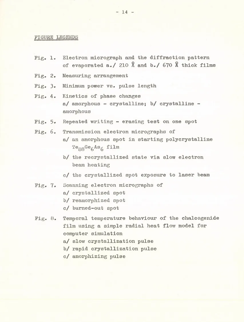
FIGURE LEGENDE
Fig. 1. Electron micrograph and the diffraction pattern of evaporated a./ 210 ft and b./ 670 ft thick films Fig. 2. Measuring arrangement
Fig. 3. Minimum power vs. pulse length Fig. 4. Kinetics of phase changes
a/ amorphous - crystalline; Ъ/ crystalline - amorphous
Fig. 5. Repeated writing - erasing test on one spot Fig. 6. Transmission electron micrographs of
a/ an amorphous spot in starting polycrystalline TeggGegAsg film
b/ the recrystallized state via slow electron beam heating
с/ the crystallized spot exposure to laser beam Fig. 7. Scanning electron micrographs of
a/ crystallized spot b/ reamorphized spot с/ burned-out spot
Fig. 8. Temporal temperature behaviour of the chalcogenide film using a simple radial heat flow model for computer simulation
a/ slow crystallization pulse b/ rapid crystallization pulse с/ amorphizing pulse
Fig. 1
m odulator p rism . lens lens
imp. generator oscilloscope x - t re c o rd e r
Fig. 2
Laser/ mW/
A
0.2 sec/divВ
F i g . 4
F i g . 8
I
'
I
I
Kiadja a Központi Fizikai Kutató Intézet Felelős kiadó: Kosa Somogyi István, a KFKI Szilárdtestkutatási Tudományos Tanácsának szekcióelnöke
Szakmai lektor : Grüner György Nyelvi lektor : H. Shenker
Példányszám: 290 Törzsszám: 76-20 Készült a KFKI sokszorosító üzemében Budapest, 1976. január hó