Electrodeposition of Hole-Transport Layer on Methylammonium Lead Iodide Film: A Strategy To Assemble Perovskite Solar Cells
Gergely F. Samu,
†,‡,⊥Rebecca A. Scheidt,
†,∥Gary Zaiats,
†,∥Prashant V. Kamat,*
,†,∥and Csaba Janáky*
,‡,§,⊥†Radiation Laboratory, University of Notre Dame, Notre Dame, Indiana 46556, United States
‡Department of Physical Chemistry and Materials Science, University of Szeged, Rerrich Square 1, Szeged H-6720, Hungary
§MTA-SZTE“Lendület”Photoelectrochemistry Research Group, Rerrich Square 1, Szeged H-6720, Hungary
∥Department of Chemistry and Biochemistry, University of Notre Dame, Notre Dame, Indiana 46556, United States
⊥ELI-ALPS Research Institute, Dugonics Square 13, Szeged 6720, Hungary
*S Supporting Information
T
he emergence of organic−inorganic metal halide perov- skites as active components in solar cells has sparked a great interest in the scientific community. A steep rise was witnessed in the power conversion efficiencies, which currently peaks at a certified value of 22.7%.1The attractiveness of these materials resides in their exceptional defect tolerance,2,3 tunable light absorption and emission properties,4,5 enhanced charge carrier transport and lifetime,4 and cost-effective preparation and processability.6 Applications beyond solar cells have also been studied, in light emitting diodes,7,8lasers,8 photodetectors,9,10X-ray detectors,11γ-detectors,12and smart windows.13Several research groups have focused on the synthesis of new organic hole-transporting materials (HTMs) for perovskite solar cells (PSCs).14−16 An emerging class of HTMs is the family of organic polymers, which inherently possesses higher hole mobility than dopant-free small molecules.16Interestingly, this growing interest has not been accompanied by the growth in the arsenal of deposition techniques. To date, spin-coating remains the preferred choice to deposit such hole conducting polymerfilms.
In a n−i−p PSC design, hole conducting layers, mainly consisting of polymeric materials (e.g., P3HT17−19 and PTAA19) that are soluble in perovskite antisolvents are studied. Although it was demonstrated that PEDOT accepts holes as effectively as spiro-OMeTAD,20its use apart from a few examples,21−23has been restricted to inverted SC designs (p−i−n junction). The direct spin-coating of the aqueous PEDOT:PSS solution is not a good option because it is known to degrade the perovskite layer. The inverted designs, however, pose further challenges such as overcoming the energy mismatch between FTO/PEDOT and attaining adequate surface coverage of the perovskite layer, which is determined by the morphology of the underlying PEDOT.
Although electrochemical deposition of the HTM layer has shown promising results in the case of dye-sensitized solar cells,24 it remained an elusive task for the n−i−p PSC architecture up to this point. This is mainly because of the instability of MAPbI3 in polar solvents,25 in which most electrochemical syntheses are carried out. Further complica- tions arise from the dynamic exchange between the cations and halide ions in the perovskite layer and those present in the
electrolyte. Such an exchange of ions can significantly alter the composition of the perovskite layer.26 It has been demon- strated recently that the electrochemical properties of MAPbI327−29 and related materials30−34 can be studied in dichloromethane based electrolytes. Special care must be exercised while conducting electrodeposition, because an external electrochemical bias can induce unintended side reactions (e.g., corrosion of the perovskite layer).29However, by implementing carefully controlled conditions, one can employ electrodeposition as a technique and utilize its superior control over several efficiency-determining factors (e.g., morphology, regularity, conductivity, optical absorption, and layer thickness).24
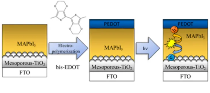
In this study, we report the electrochemical deposition of PEDOT (HTM layer) directly on the MAPbI3film deposited on a FTO/TiO2 electrode and its implementation in a perovskite solar cell (PSC) with an n−i−p architecture (Scheme 1). The effect of electrochemical post-treatments of the HTM layer on the performance of PSC has also been scrutinized.
■
RESULTS AND DISCUSSIONElectropolymerization of Hole-Transport Layer. The first step was to ensure that the MAPbI3layer remains intact during the electropolymerization. FTO/TiO2/MAPbI3electro-
Received: April 12, 2018 Revised: June 12, 2018 Published: June 12, 2018
Scheme 1. Illustration of the Assembly and Operation of the Perovskite Solar Cell with PEDOT Hole-Transporter
Communication pubs.acs.org/cm Cite This:Chem. Mater.2018, 30, 4202−4206
copying and redistribution of the article or any adaptations for non-commercial purposes.
Downloaded via 160.114.21.80 on December 4, 2018 at 13:45:47 (UTC). See https://pubs.acs.org/sharingguidelines for options on how to legitimately share published articles.
des with a thin MAPbI3layer were fabricated to monitor the optical changes during electrochemical deposition of the HTM layer, as described in the Supporting Information. The time frame of the experiment and potential-range of the PEDOT electrodeposition (in the absence of bis-EDOT monomer) was established through prolonged immersion of the FTO/TiO2/ MAPbI3 electrode in the solvent and carrying out cyclic voltammetric experiments. As established in our earlier methods and protocol work,29 0.1 M Bu4NPF6 in dichloro- methane offers the best electrochemical condition as no significant change in the overall shape of the optical absorption of the perovskite film is observed after 10 min of exposure (Figure S1A). As for the electrochemical properties, MAPbI3 layers were more resistant to oxidation than reduction (Figure S1B). Top-down and cross-sectional SEM images as well as XPS studies confirmed the stability of the FTO/TiO2/MAPbI3 electrodes during both immersion in the electrolyte and oxidative biasing, up to 1.1 V (Figures S2andS3). However,
EDOT cannot be used as the polymerization precursor, because its polymerization (oxidation) potential would exceed the electrochemical stability of MAPbI3layers. To overcome this limitation, we employed bis-EDOT as a precursor (Scheme S1). The use of bis-EDOT, in turn, allowed us to carry out the (oxidative) electropolymerization and produce PEDOTfilms without degrading the MAPbI3layer.35
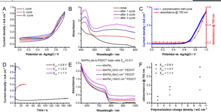
The electropolymerization process initiated by the electro- chemical oxidation of bis-EDOT on FTO/TiO2/MAPbI3 electrodes was monitored usingin situspectroelectrochemical experiments (Figure 1A−C). The gradual growth of PEDOT during potentiodynamic deposition was evident from the change in absorption as well as the increasing (pseudo)- capacitive current in the potential range of 0.0−0.6 V. The absorption peak at 450 nm was attributed to EDOT oligomers and the broad absorption in the 500−800 nm region (Figure 1B) was assigned to the polymer product, viz., PEDOT layer.
To correlate the polymer formation with the oxidation of bis- Figure 1.(A) Potentiodynamic deposition of PEDOT with 25 mV s−1sweep rate in a 0.01 M bis-EDOT, 0.1 M Bu4NPF6DCM on a PSC architecture (FTO/bl-TiO2/mp-TiO2/MAPbI3) employing a thin MAPbI3layer. (B) UV−vis absorbance spectra recorded after each cycle atE= 0.0 V during polymerization. (C) First half-cycle of the potentiodynamic deposition plotted together with the absorbance change at 700 nm. (D) Potentiostatic deposition of PEDOT at different potentials in a 0.01 M bis-EDOT, 0.1 M Bu4NPF6 DCM solution on a PSC architecture employing regular thickness MAPbI3layers with a polymerization charge density of 10 mC cm−2. (E) UV−vis absorbance spectra of PSCs after PEDOT electrodeposition atE= 0.9 V for different polymerization charge densities. (F) Absorbance change of the PSCs compared to a HTM-free cell by varying the polymerization charge density at different applied potentials.
Figure 2.(A) Top-view SEM image before (upper part) and after PEDOT (lower part) electrodeposition and (B) cross-sectional FIB-SEM image of a PSC, where the PEDOT electrodeposition was carried out atE= 1.0 V withQpol= 5 mC cm−2. (C) Theoretical and actual PEDOT layer thicknesses (determined from cross-sectional SEM images). (D) Raman-spectra of a fully assembled FTO/TiO2/MAPbI3/PEDOT architecture and a FTO/PEDOT reference material.
Chemistry of Materials
EDOT, the current density of the first polymerization half cycle was plotted along with the absorbance increase at 700 nm (Figure 1C). A sharp rise in the current at 0.7 V was accompanied by the absorbance increase at 700 nm, thus confirming the polymerization of bis-EDOT.
Although polymerization starts at 0.7 V, prolonged exposure to the electrolyte needs to be avoided. As shown inFigure 1D, adequate polymerization rate was achieved at potentials above 0.9 V. In addition, by varying the electrochemical charge density, the thickness of the formed PEDOT layer can befine- tuned, as deduced from the absorbance spectra (Figure 1E,F).
The UV−vis absorption features did not indicate any noticeable changes corresponding to perovskite layer absorp- tion, thereby confirming the conservation of original MAPbI3 architecture during the electropolymerization process.
Characterization of PEDOT Layer.SEM images captured the morphological features of the PEDOT layers on the MAPbI3film following the deposition of PEDOT at 1.0 V with Qpol = 5 mC cm−2. The top-view images show that the electropolymerized layer of PEDOT completely covers the MAPbI3layer (Figure 2A). The smooth MAPbI3surface was not visible anymore, instead a furry polymer coating developed. These images confirmed the homogeneity of the PEDOT layer and that the MAPbI3remained intact during the electrodeposition. In order to determine the thickness of the formed PEDOT, cross-sectional FIB-SEM images were recorded (Figure 2B). The measured PEDOT thickness was compared with the value, calculated from the charge density employed during polymerization (Figure 2C). These values fall in the range of the HTM thicknesses (40−300 nm) employed in the case of MAPbI3 PSCs using PEDOT.21,22 Raman- spectroscopic studies (Figure 2D) further confirmed the characteristics of an electrochemically deposited PEDOT on top of the MAPbI3layer.
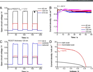
Post-treatment of PEDOT Layer.The doping level of the HTL is important for optimization of PSCs. When we evaluated the photovoltaic performance of the MAPbI3PSCs employing the electrochemically deposited PEDOT hole- transporting layers, without any post-treatment (see Support- ing Informationfor detailed analysis (Figure S4)), all of them exhibited low open circuit voltage (VOC) (Figure 3A) andfill factor (FF). The inability of PEDOT layer to transport the holes efficiently results in increased charge recombination (Figure S4). One way to overcome these issues is to modulate the doping level of PEDOT layer. We employed electro- chemical post-treatment approach to alter the doping level (Scheme S2). PEDOTfilms deposited at 1.0 V, with aQpol = 3−10 mC cm−2 seemed to be optimal to evaluate post- treatment conditions. This reductive post-treatment method, however, had an unintended side-effect, as revealed by cross- sectional SEM images (Figure S5A,B). Though the reduction of PEDOT is beneficial for its performance, it destroys some of the MAPbI3 from the underlying layer. Three different strategies were employed to mitigate this effect: (i) rapid reduction at−0.6 V for 10 s (Figure S6A); (ii) mild reduction at−0.5 V for 60 s (Figure S6B); and (iii) rapid-mild reduction at−0.5 V for 20 s (Figure S6C).
There was an improvement in the VOC of the devices compared to the untreated PEDOT in all cases (Figure S7), but the JSCand the FF remained low in most cases (Figure S9A−D). The only exception was the rapid reduction, where the champion cell had a 5.9% efficiency (Figure 3D). Top- down and cross-sectional SEM images recorded for samples
post-treated with the rapid reduction revealed that the degradation of the MAPbI3 layers can be avoided using this strategy (Figure S8).
Transient Absorption Measurements. To probe the hole accepting ability of PEDOT, transient absorption spectroscopic measurements were carried out (Figure 4A).
The characteristics of the spectra are in good accordance with MAPbI3 spectra in the literature.36 The most prominent feature, the ground state bleach at 760 nm, is caused by charge separation due to band edge transition in MAPbI3.36 Furthermore, there is no additional bleaching signal present at∼500 nm that would arise from PbI2in the material. The recovery of the 760 nm bleach follows second-order kinetics (Figure 4B). Fitting the data to a biexponential decay reveals that the average lifetime (seeSupporting Informationfor the calculations and detailed analysis) has the following trend:
reduced PEDOT (tweighed avg = 1280 ps) < as-is PEDOT (tweighed avg= 1660 ps) < no HTM (tweighed avg= 1750 ps). The shorter lifetime indicates the transfer of photogenerated holes Figure 3. (A) Effect of PEDOT thickness (polymerization charge density) on the open circuit voltage in a FTO/TiO2/MAPbI3/ PEDOT PSC for PEDOT layers electrodeposited atE = 1.0 V. (B) Chronoamperometric curves recorded for the PEDOT layers electrodeposited atE= 1.0 V, when a reductive post-treatment atE
=−0.6 V was employed. (C) Buildup of the open circuit potential in a FTO/TiO2/MAPbI3/PEDOT SC for the PEDOT layers electro- deposited atE= 1.0 V forQpol= 10 mC cm−2. (D)J−Vcurve of the champion device containing a PEDOT layer electrodeposited atE= 1.0 V forQpol= 10 mC cm−2, where the postreduction step was atE=
−0.6 V fort= 10 s.
Figure 4. (A) Time-resolved transient spectra of an FTO/TiO2/ MAPbI3/PEDOT PSC employing a thin MAPbI3 layer recorded following 387 nm laser pulse excitation. The PEDOT layer was prepared and post-treated just as the champion device. (B) Bleaching recovery profiles at 760 nm of different FTO/TiO2/MAPbI3/PEDOT PSCs.
Chemistry of Materials
from MAPbI3 layer to PEDOT layer. Furthermore, the postsynthetic reduction technique improves the hole accepting properties of the PEDOTfilm.
■
CONCLUSIONSThe electrochemical deposition of PEDOT offers a convenient way to deposit a hole-transport layer on a MAPbI3layer for designingn−i−pjunction perovskite solar cells. By employing potentiostatically controlled electrodeposition technique, it is possible to obtain controlled thicknesses of HTM layers. An electrochemical postreduction step introduced to control the doping level of the as-deposited PEDOTfilms is an essential step in achieving better performance of PSCs. Care should be exercised not to destroy the underlying MAPbI3 layer during the post-treatment process. The champion device showed a power conversion efficiency of 5.9%. The results presented in this study open new opportunities to employ electrochemistry to assemble complex architectures of optically active perov- skites.
■
ASSOCIATED CONTENT*S Supporting Information
The Supporting Information is available free of charge on the ACS Publications website at DOI: 10.1021/acs.chemma- ter.8b01521.
Detailed synthesis and characterization procedures, electrochemical stability tests, solar cell characterization parameters derived from J−V curves, SEM-FIB images of solar cells, current transients recorded during electrochemical reduction,fitting parameters of transient absorption spectra (PDF)
■
AUTHOR INFORMATION Corresponding Authors*P. V. Kamat. E-mail: pkamat@nd.edu. Twitter:
@kamatlabND.
*C. Janáky. E-mail: janaky@chem.u-szeged.hu. Twitter:
@JanakyLab.
ORCID
Prashant V. Kamat:0000-0002-2465-6819
Csaba Janáky: 0000-0001-5965-5173 Notes
The authors declare no competingfinancial interest.
■
ACKNOWLEDGMENTSThe authors thank Dr. Gábor London (Univ Szeged) for synthesizing the bis-EDOT monomer as well as Dr. Tatyana Orlova and the Notre Dame Integrated Imaging Facility for taking the SEM images. This project has received funding from the European Research Council (ERC) under the European Union’s Horizon 2020 research and innovation program (grant agreement no. 716539). ELI-ALPS is supported by the European Union and cofinanced by the European Regional Development Fund (GOP-1.1.1-12/B-2012-000, GINOP- 2.3.6-15-2015-00001). P.V.K. acknowledges support by the Division of Chemical Sciences, Geosciences, and Biosciences, Office of Basic Energy Sciences of the U.S. Department of Energy (award DE-FC02-04ER15533). R.S. acknowledges support of King Abdullah University of Science and Technology (KAUST-Award OCRF-2014-CRG3-2268). This
is contribution number NDRL No. 5213 from the Notre Dame Radiation Laboratory.
■
(1) Yang, W. S.; Park, B.-W.; Jung, E. H.; Jeon, N. J.; Kim, Y. C.; Lee,REFERENCES D. U.; Shin, S. S.; Seo, J.; Kim, E. K.; Noh, J. H.; Seok, S., Il Iodide Management in Formamidinium-Lead-Halide−based Perovskite Layers for Efficient Solar Cells.Science2017,356, 1376−1379.(2) Huang, H.; Bodnarchuk, M. I.; Kershaw, S. V.; Kovalenko, M. V.;
Rogach, A. L. Lead Halide Perovskite Nanocrystals in the Research Spotlight: Stability and Defect Tolerance.ACS Energy Lett.2017,2, 2071−2083.
(3) Swarnkar, A.; Ravi, V. K.; Nag, A. Beyond Colloidal Cesium Lead Halide Perovskite Nanocrystals: Analogous Metal Halides and Doping.ACS Energy Lett.2017,2, 1089−1098.
(4) Manser, J. S.; Christians, J. A.; Kamat, P. V. Intriguing Optoelectronic Properties of Metal Halide Perovskites. Chem. Rev.
2016,116, 12956−13008.
(5) Minh, D. N.; Kim, J.; Hyon, J.; Sim, J. H.; Sowlih, H. H.; Seo, C.;
Nam, J.; Eom, S.; Suk, S.; Lee, S.; Kim, E.; Kang, Y. Room- Temperature Synthesis of Widely Tunable Formamidinium Lead Halide Perovskite Nanocrystals.Chem. Mater.2017,29, 5713−5719.
(6) Manser, J. S.; Saidaminov, M. I.; Christians, J. A.; Bakr, O. M.;
Kamat, P. V. Making and Breaking of Lead Halide Perovskites.Acc.
Chem. Res.2016,49, 330−338.
(7) Pathak, S.; Sakai, N.; Wisnivesky Rocca Rivarola, F.; Stranks, S.
D.; Liu, J.; Eperon, G. E.; Ducati, C.; Wojciechowski, K.; Griffiths, J.
T.; Haghighirad, A. A.; Pellaroque, A.; Friend, R. H.; Snaith, H. J.
Perovskite Crystals for Tunable White Light Emission.Chem. Mater.
2015,27, 8066−8075.
(8) Veldhuis, S. A.; Boix, P. P.; Yantara, N.; Li, M.; Sum, T. C.;
Mathews, N.; Mhaisalkar, S. G. Perovskite Materials for Light- Emitting Diodes and Lasers.Adv. Mater.2016,28, 6804−6834.
(9) Wang, H.; Kim, D. H. Perovskite-Based Photodetectors:
Materials and Devices.Chem. Soc. Rev.2017,46, 5204−5236.
(10) Ahmadi, M.; Wu, T.; Hu, B. A Review on Organic-Inorganic Halide Perovskite Photodetectors: Device Engineering and Funda- mental Physics.Adv. Mater.2017,29, 1605242.
(11) Yakunin, S.; Sytnyk, M.; Kriegner, D.; Shrestha, S.; Richter, M.;
Matt, G. J.; Azimi, H.; Brabec, C. J.; Stangl, J.; Kovalenko, M. V.;
Heiss, W. Detection of X-Ray Photons by Solution-Processed Lead Halide Perovskites.Nat. Photonics2015,9, 444−449.
(12) Yakunin, S.; Dirin, D. N.; Shynkarenko, Y.; Morad, V.;
Cherniukh, I.; Nazarenko, O.; Kreil, D.; Nauser, T.; Kovalenko, M. V.
Detection of Gamma Photons Using Solution-Grown Single Crystals of Hybrid Lead Halide Perovskites.Nat. Photonics2016,10, 585−589.
(13) De Bastiani, M.; Saidaminov, M. I.; Dursun, I.; Sinatra, L.;
Peng, W.; Buttner, U.; Mohammed, O. F.; Bakr, O. M.
Thermochromic Perovskite Inks for Reversible Smart Window Applications.Chem. Mater.2017,29, 3367−3370.
(14) Ameen, S.; Rub, M. A.; Kosa, S. A.; Alamry, K. A.; Akhtar, M.
S.; Shin, H.-S.; Seo, H.-K.; Asiri, A. M.; Nazeeruddin, M. K. Perovskite Solar Cells: Influence of Hole Transporting Materials on Power Conversion Efficiency.ChemSusChem2016,9, 10−27.
(15) Völker, S. F.; Collavini, S.; Delgado, J. L. Organic Charge Carriers for Perovskite Solar Cells.ChemSusChem 2015, 8, 3012−
3028.
(16) Bakr, Z. H.; Wali, Q.; Fakharuddin, A.; Schmidt-Mende, L.;
Brown, T. M.; Jose, R. Advances in Hole Transport Materials Engineering for Stable and Efficient Perovskite Solar Cells. Nano Energy2017,34, 271−305.
(17) Zhang, Y.; Liu, W.; Tan, F.; Gu, Y. The Essential Role of the poly(3-Hexylthiophene) Hole Transport Layer in Perovskite Solar Cells.J. Power Sources2015,274, 1224−1230.
(18) Di Giacomo, F.; Razza, S.; Matteocci, F.; D’Epifanio, A.;
Licoccia, S.; Brown, T. M.; Di Carlo, A. High Efficiency CH3NH3PbI(3−x)Clx Perovskite Solar Cells with poly(3-Hexylthio- phene) Hole Transport Layer.J. Power Sources2014,251, 152−156.
Chemistry of Materials
(19) Heo, J. H.; Im, S. H.; Noh, J. H.; Mandal, T. N.; Lim, C.-S.;
Chang, J. A.; Lee, Y. H.; Kim, H.; Sarkar, A.; Nazeeruddin, M. K.;
Grätzel, M.; Seok, S., Il Efficient Inorganic−organic Hybrid Heterojunction Solar Cells Containing Perovskite Compound and Polymeric Hole Conductors.Nat. Photonics2013,7, 486−491.
(20) Docampo, P.; Ball, J. M.; Darwich, M.; Eperon, G. E.; Snaith, H. J. Efficient Organometal Trihalide Perovskite Planar-Hetero- junction Solar Cells on Flexible Polymer Substrates.Nat. Commun.
2013,4, 2761.
(21) Koushik, D.; Verhees, W. J. H.; Zhang, D.; Kuang, Y.; Veenstra, S.; Creatore, M.; Schropp, R. E. I. Atomic Layer Deposition Enabled Perovskite/PEDOT Solar Cells in a Regular N-I-P Architectural Design.Adv. Mater. Interfaces2017,4, 1700043.
(22) Liu, J.; Pathak, S.; Stergiopoulos, T.; Leijtens, T.;
Wojciechowski, K.; Schumann, S.; Kausch-Busies, N.; Snaith, H. J.
Employing PEDOT as the P-Type Charge Collection Layer in Regular Organic−Inorganic Perovskite Solar Cells.J. Phys. Chem. Lett.
2015,6, 1666−1673.
(23) Jiang, X.; Yu, Z.; Zhang, Y.; Lai, J.; Li, J.; Gurzadyan, G. G.;
Yang, X.; Sun, L. High-Performance Regular Perovskite Solar Cells Employing Low-Cost Poly(ethylenedioxythiophene) as a Hole- Transporting Material.Sci. Rep.2017,7, 42564.
(24) Janáky, C.; Rajeshwar, K. The Role of (Photo)electrochemistry in the Rational Design of Hybrid Conducting Polymer/semi- conductor Assemblies: From Fundamental Concepts to Practical Applications.Prog. Polym. Sci.2015,43, 96−135.
(25) Gardner, K. L.; Tait, J. G.; Merckx, T.; Qiu, W.; Paetzold, U.
W.; Kootstra, L.; Jaysankar, M.; Gehlhaar, R.; Cheyns, D.; Heremans, P.; Poortmans, J. Nonhazardous Solvent Systems for Processing Perovskite Photovoltaics.Adv. Energy Mater.2016,6, 1600386.
(26) Shewmon, N. T.; Yu, H.; Constantinou, I.; Klump, E.; So, F.
Formation of Perovskite Heterostructures by Ion Exchange. ACS Appl. Mater. Interfaces2016,8, 33273−33279.
(27) Hsu, H.-Y.; Ji, L.; Ahn, H. S.; Zhao, J.; Yu, E. T.; Bard, A. J. A Liquid Junction Photoelectrochemical Solar Cell Based on P-Type MeNH3PbI3 Perovskite with 1.05 V Open-Circuit Photovoltage. J.
Am. Chem. Soc.2015,137, 14758−14764.
(28) Hsu, H.-Y.; Ji, L.; Du, M.; Zhao, J.; Yu, E. T.; Bard, A. J.
Optimization of PbI2/MAPbI3 Perovskite Composites by Scanning Electrochemical Microscopy. J. Phys. Chem. C 2016, 120, 19890− 19895.
(29) Samu, G. F.; Scheidt, R. A.; Kamat, P. V.; Janáky, C.
Electrochemistry and Spectroelectrochemistry of Lead Halide Perov- skite Films: Materials Science Aspects and Boundary Conditions.
Chem. Mater.2018,30, 561−569.
(30) Shallcross, R. C.; Zheng, Y.; Saavedra, S. S.; Armstrong, N. R.
Determining Band-Edge Energies and Morphology-Dependent Stability of Formamidinium Lead Perovskite Films Using Spectroelec- trochemistry and Photoelectron Spectroscopy. J. Am. Chem. Soc.
2017,139, 4866−4878.
(31) Hsu, H.-Y.; Ji, L.; Du, M.; Zhao, J.; Yu, E. T.; Bard, A. J.
Optimization of Lead-Free Organic-Inorganic Tin(II) Halide Perov- skite Semiconductors by Scanning Electrochemical Microscopy.
Electrochim. Acta2016,220, 205−210.
(32) Li, Z.; Mercado, C. C.; Yang, M.; Palay, E.; Zhu, K.
Electrochemical Impedance Analysis of Perovskite-Electrolyte Inter- faces.Chem. Commun.2017,53, 2467−2470.
(33) Scheidt, R. A.; Samu, G. F.; Janáky, C.; Kamat, P. V.
Modulation of Charge Recombination in CsPbBr3 Perovskite Films with Electrochemical Bias.J. Am. Chem. Soc.2018,140, 86−89.
(34) Ravi, V. K.; Markad, G. B.; Nag, A. Band Edge Energies and Excitonic Transition Probabilities of Colloidal CsPbX3(X = Cl, Br, I) Perovskite Nanocrystals.ACS Energy Lett.2016,1, 665−671.
(35) Samu, G. F.; Visy, C.; Rajeshwar, K.; Sarker, S.; Subramanian, V. R.; Janáky, C. Photoelectrochemical Infiltration of a Conducting Polymer (PEDOT) into Metal-Chalcogenide Decorated TiO2 Nanotube Arrays.Electrochim. Acta2015,151, 467−476.
(36) Stamplecoskie, K. G.; Manser, J. S.; Kamat, P. V. Dual Nature of the Excited State in Organic−inorganic Lead Halide Perovskites.
Energy Environ. Sci.2015,8, 208−215.
Chemistry of Materials
![BasedontheEUROSTATdatabase[ ],theshareofenergyproducedbyrenewablesources sustainableenergy.AccordingtoWolsink[ ],policymakersandresearcherspresentrenewablesasasolutiontoenvironmentalproblems,particularlyglobalissueslinkedtofossilfuelsandnuclearpower.Botht](data:image/gif;base64,R0lGODlhAQABAIAAAP///wAAACH5BAEAAAAALAAAAAABAAEAAAICRAEAOw==)