Tuning the Excited-State Dynamics of CuI Films with Electrochemical Bias
Gergely F. Samu,*
,†,‡,∥Rebecca A. Scheidt,
†,§A ́ dám Balog,
‡Csaba Janáky,*
,‡,∥and Prashant V. Kamat*
,†,§†Radiation Laboratory, University of Notre Dame, Notre Dame, Indiana 46556, United States
‡Department of Physical Chemistry and Materials Science, Interdisciplinary Excellence Centre, University of Szeged, Rerrich Square 1, Szeged H-6720, Hungary
§Department of Chemistry and Biochemistry, University of Notre Dame, Notre Dame, Indiana 46556, United States
∥ELI-ALPS Research Institute, Dugonics Square 13, Szeged 6720, Hungary
*S Supporting Information
ABSTRACT: Owing to its high hole conductivity and ease of preparation, CuI was among thefirst inorganic hole-transporting materials that were introduced early on in metal halide perovskite solar cells, but its full potential as a semiconductor material is still to be realized. We have now performed ultrafast spectroelectrochemical experiments on ITO/CuI electrodes to show the effect of applied bias on the excited-state dynamics in CuI. Under operating conditions, the recombination of excitons is dependent on the applied bias, and it can be accelerated by decreasing the potential from +0.6 to −0.1 V vs Ag/AgCl.
Prebiasing experiments show the persistent and reversible “memory” effect of electrochemical bias on charge carrier lifetimes. The excitation of CuI in a CuI/CsPbBr3film provides synergy between both CuI and CsPbBr3in dictating the charge separation and recombination.
T
he recent surge of interest in organic−inorganic hybrid perovskites has drawn considerable attention to related materials that are essential to assemble high-perform- ance perovskite solar cells (PSCs).1,2An increasing emphasis is given to the charge transport properties of the electron- and hole-transporting materials (ETMs and HTMs, respectively)3 and the quality of the formed interfaces.4−6 The top- performing PSCs mainly utilize organic small molecules or polymeric HTMs,7−10 but their inorganic counterparts offer increased stability and superior device properties (e.g., suppressed hysteresis).11Copper-based inorganic compounds (e.g., CuI,12−17CuSCN,18−21CuOx,22,23and CuCrO224,25) are especially promising candidates even though their use is inhibited by their lack of suitable solution deposition methods that produce uniform, compact, and crack-free layers. Recently, PSCs employing CuSCN as the HTM have achieved stabilized efficiencies exceeding 20% over 1000 h of continuous illumination, which is superior to spiro-OMeTAD-based devices.21 Interestingly, the spotlight has avoided CuI as a HTM so far despite the fact that it possesses hole mobility two magnitudes greater than that of CuSCN.11 Furthermore, device modeling studies suggest that comparable efficiencies to CuSCN-based devices can be achieved, also overcoming the 20% threshold.26CuI is a transparent wide-bandgap (3.0 eV) p-type semiconductor, with a large exciton binding energy of 62 meV.27Low-temperature preparation techniques can be used to prepare high-quality CuIfilms such as spin-coating,13,15,28 inkjet printing,29 spray coating,17 or iodination of Cu/CuN3 precursors.30−32 The band structure, which has considerable contributions from iodide orbitals, allows for an acceptor level near the valence band edge, leading to greater hole mobility in halide-based cuprous materials than their oxide counterparts.30 This results in remarkable hole conductivity in CuI single crystals,33up to 43.9 cm2V−1s−1with a hole concentration of 4.3×1016cm−3. For annealed polycrystalline thinfilms, a hole conductivity greater than 20 cm2V−1s−1was achieved.31,32,34 Previous studies have examined the underlying mechanism of increased hole mobility, indicating that iodide and copper vacancies at grain boundaries30as well as hole accumulation layers due to interfacial defect band formations are the cause.35 Recently, we revealed the effect of trap states on the optoelectronic properties of CuI electrodes using spectroelec- trochemistry.36 It was shown that the population of shallow trap states affects the optical properties of CuI layers, while the
Received: January 24, 2019 Accepted: February 13, 2019 Published: February 13, 2019
Letter
http://pubs.acs.org/journal/aelccp Cite This:ACS Energy Lett.2019, 4, 702−708
copying and redistribution of the article or any adaptations for non-commercial purposes.
Downloaded by UNIV OF SZEGED at 03:20:06:735 on July 09, 2019 from https://pubs.acs.org/doi/10.1021/acsenergylett.9b00182.
filling of deep trap states alters the electrical properties of the CuI layers.36
To the best of our knowledge, studies on the excited-state dynamics in CuIfilms are still lacking. Tofill this gap and to better understand the effect of external bias on the recombination kinetics of charge carriers (or excitons) in CuI, we carried out ultrafast spectroelectrochemical measure- ments.37,38 This technique was used to study oxidation mechanisms on oxide semiconductors in different (photo)- electrochemical reactions.39−42We aimed to probe the effect of in situ trap state filling on the fate of charge carriers.
Additionally, ex situ relaxation experiments were performed on precharged CuI electrodes. Preliminary studies on CuI/
CsPbBr3 interfaces are also shown as an outlook to the application of CuI in PSCs.
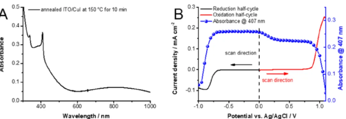
Stability Window of ITO/CuI Electrodes.CuIfilms cast on an ITO electrode (ITO/CuI) and annealed at 150°C for 10 min exhibit two absorption bands at 338 and 407 nm, which are in good agreement with literature values.27 These sharp absorption bands are attributed to excitonic transitions (Figure 1A).27The broad absorption band starting from 600 nm can be attributed to iodine vacancies in the crystal structure of the deposited CuI. These form trap states over the valence band of CuI. In turn, these interstitial states can induce intraband transitions with light of lower energy than the bandgap of CuI.
Direct optical excitation of a semiconductor produces electrons and holes intrinsically, whereas electrochemistry allows external injection of electrons or holes selectively into the semiconductor film. By combining electrochemistry and
spectroscopy, we can obtain unique information on the excited-state properties at various levels of electron or hole injection through applied electrochemical bias.
In the present investigation, spectroelectrochemical meas- urements were performedfirst to establish the stability window of ITO/CuI electrodes in dichloromethane (DCM) containing 0.1 M Bu4NPF6 electrolyte (Figure 1B). The absorbance change at the excitonic peak at 407 nm was plotted along with the current density during the electrochemical sweep. The excitonic peak decreases when the potential increases from 0.0 to +0.4 V vs Ag/AgCl. This decrease can be reverted upon reversing the potential scan, which is related to the reversible population/depopulation of shallow trap states, as discussed in our previous study.36The rapid decrease in the absorbance at extreme positive and negative potentials (greater than +0.80 and−0.70 V), however, is caused by degradation of the CuI film as it undergoes irreversible Faradaic processes. Thus, these two potentials define the stability window (from−0.1 to +0.6 V vs Ag/AgCl) to conduct spectroelectrochemical measure- ments with CuIfilms.
Ultrafast Spectroelectrochemistry of ITO/CuI Electrodes. The large exciton binding energy of CuI (62 meV) makes it difficult to induce charge carrier separation at room temperature following bandgap excitation. Thus, the recovery of the bleach in the transient absorption (TA) spectra seen at 406 nm is attributed to the recovery of the exciton band. Previous reports have shown that the exciton band of semiconducting materials can be reversibly altered with applied electrochemical bias due to the enhanced separation of excitons and/or band filling Figure 1. (A) UV−vis absorbance spectrum of the ITO/CuI electrode, annealed at 150°C for 10 min. (B) Spectroelectrochemical data, recorded for ITO/CuI electrodes in 0.1 M Bu4NPF6/DCM electrolyte (5 mV s−1 sweep rate). The cathodic and anodic half-cycles were recorded on separate electrodes. The absorbance of the excitonic peak at 407 nm is plotted together with the recorded current during the half-cycles.
Figure 2. (A) Time-resolved TA spectra of ITO/CuI electrodes in 0.1 M Bu4NPF6/DCM electrolyte after 387 nm laser pulse excitation (4μJ cm−2) at an applied potential of +0.2 V vs Ag/AgCl. (B) Bleach recovery profiles monitored at 412 nm at applied potentials from−0.1 to +0.6 V vs Ag/AgCl. (C) Potential dependence of the determined lifetimes. The recovery profiles in (B) werefitted with a monoexponential decay. The error bars represent measurements on three separate electrodes.
effects.43−45Using this knowledge, we probed the excited-state dynamics of CuI under applied bias in order to elucidate excitonic behavior. In our systematic approach, we carried out control experiments first, to show that the presence of the electrolyte has no effect on the time-resolved spectral characteristics of ITO/CuI film electrodes (Figure S1A,B).
At the same time, in the electrolyte, a slightly slower recovery of the bleach signal was observed under open-circuit conditions (Figure S1C). This can be attributed to the double-layer charging near the electrode surface. The TA spectra of ITO/CuI electrodes consist of two induced absorption (IA) bands (IA1 at 399 nm and IA2 at 419 nm) and two bleaching signals (PB1 at 408 nm and PB2 at 412 nm) shown inFigure 2A. The IA1 band located at higher energies likely arises from the absorption of the lowest excitonic state, and the IA2 is from the absorption of hot excitons.46
While the majority of the excitation involves exciton formation followed by recombination (reactions 1 and 2), a small fraction can undergo charge separation, especially in the presence of electrolyte (reaction 3). The shorter lifetime in the presence of electrolyte supports such an argument. One plausible explanation for the presence of two bleaching signals involves excitons consisting of light (PB2) and heavy (PB1) holes, caused by strains in the material.47The expected energy difference is 20 meV according to literature data.47From the TA spectra, 30 meV of difference was calculated between the two bleach signals, validating the proposed scenario.
+hν→ ···
CuI Cul(h e) (1)
··· →
CuI(h e) CuI (2)
··· → +
CuI(h e) CuI(h e) (3)
To study the effect of applied bias on the kinetics of exciton recombination, the ITO/CuI electrodes were held at different potentials within the stability window (from +0.6 to−0.1 V vs Ag/AgCl). Both bleach recoveries showed similar potential dependence; thus, for the sake of simplicity, only the recovery profiles for the PB2 are shown inFigure 2B. The kinetic traces show a monoexponential decay (first-order kinetics), which is the result of direct exciton recombination (reaction 2) and charge separation (reaction 3). The time constant of this monoexponential decay can be given by the reverse sum of the rate of these two processes. Note, however, that the large exciton binding energy (62 meV) of CuI does not favor charge
separation at room temperature; thus, only a small fraction of excitons can undergo separation.27
As we change the applied potential from +0.6 to−0.1 V vs Ag/AgCl, a faster bleach recovery is observed (Figure 2C).
This translates to a decrease in the lifetime from 5.2 to 1.1 ps.
With increased negative bias, electron injection to CuI takes place, whichfills the trap states in the material. As these vacant energy states are filled, charge carrier trapping is suppressed;
thus, a decrease of the lifetime of free charge carriers is expected. In addition, as a secondary effect, the external driving force might facilitate the dissociation of excitons. This introduces new pathways for the ground state to be repopulated such as direct recombination of free charge carriers and recombination at the ITO/CuI interface. The slight tailing (distortion of the monoexponential decay) on the kinetic traces inFigure 2B at more negative bias signals this scenario. We performed thefit of all of the kinetic traces to monoexponential decay as the longer component has only a minor contribution to the overall decay.
Reversibility of Exciton Dissociation in ITO/CuI Electrodes.
Interestingly, the observed decrease in excited-state lifetime of CuI was reversible. When the applied bias was reversed, we saw an increasing trend in the lifetime. The TA spectra recorded under a forward (−0.1 to +0.6 V vs Ag/AgCl) scan followed by a reverse scan (+0.6 to−0.1 V vs Ag/AgCl) are shown in the Supporting Information (Figure S2). The kinetic traces corresponding to the bleaching recovery (PB2 signal) at 0.0 and +0.6 V vs Ag/AgCl recorded during forward and reverse scan are presented inFigure 3A. The recovery kinetics observed for all recovery profiles were fitted with a monoexponential decay. The lifetimes obtained during forward and reverse bias show the reversible trend of exciton bleach recovery lifetimes (Figure 3B). A small hysteresis in the measured lifetimes observed during these two scans is likely to arise from the residual accumulation of charges and/or slowness of the system to undergo equilibration and respond quickly to the applied bias.
Prebiasing of ITO/CuI Electrodes and Its Ef fect on Excited- State Recovery.In the case of PSCs, prebiasing or light soaking prior to current−voltage measurements has a pronounced effect on the determined efficiency.48This is mainly caused by charge accumulation at the interfaces in the solar cells.
Accumulation of ions or charged species near the electrode surface are also responsible for the observed hysteresis ofJ−V curves.49Such charge accumulation can also have a profound influence on the excited-state recovery of CuIfilms. To probe Figure 3. Reversibility studies of the effect of applied bias on the kinetics of the bleach recovery. (A) Bleaching recovery profiles monitored at 412 nm at the two end potentials of the stability window. (B) Potential dependence of the determined bleach recovery lifetimes [monoexponentialfit of kinetic traces in (A)].
ACS Energy Letters
such charging effects, we prebiased the ITO/CuI electrode for 10 min, and then, we disconnected the cell from the potentiostat. The potential difference between the semi- conductor Fermi level and the reference electrode is the measured open-circuit potential (EOCP). By modulating the electrical bias, we shift the Fermi level of CuI by populating/
depopulating trap states in the material (Scheme 1.). The
measuredEOCP of the cell (immediately after disconnection) provided an estimate of the charging effect.
Note that the EOCP is a measure of electrons/holes accumulated at the electrode. With increasing time, the electrons (or holes) are slowly discharged and the EOCP increases (or drops). Thus, by varying the delay time after releasing potential control, different equilibration of charges
aWith time, the original dark potential is achieved.
Figure 4. Bleaching recovery profiles monitored at 412 nm recorded for ITO/CuI electrodes in 0.1 M Bu4NPF6/DCM electrolyte that were charged at (A)−0.1 and (C) 0.6 V for 10 min prior to measurements. Relaxation ofEOCPof the electrodes plotted together with the change in the bleaching recovery time after prebiasing at (B)−0.1 and (D) 0.6 V.
can be attained in the ITO/CuI electrode. TA spectra were recorded with different equilibration delay times while monitoring the EOCP of the electrodes. This allowed us to independently confirm the effect of accumulated electrons/
holes on the excited-state recovery of the CuIfilm, simulating the conditions in a photoirradiated cell under open-circuit conditions.
We selected two different bias potentials (−0.1 and +0.6 V), corresponding to the end points selected in the experiments of Figure 2. TA spectra were recorded for 500 s after the bias was released. The first and last recovery traces for the 412 nm bleach during the relaxation experiment (after prebiasing at
−0.1 V) are shown in Figure 4A. Interestingly, after the bias was released, the charging effect was retained, as evident from theEOCP and the bleach recovery traces. The lifetimes (from recovery traces fitted to first-order kinetics) are plotted together with the measuredEOCP (Figure 4B). It is apparent that the recovery lifetime changes in the same fashion as the EOCP.
The prebiasing has a persistent effect for more than 100 s on both the charge carrier lifetime and EOCP of the ITO/CuI electrodes. When the layers were prebiased at 0.6 V for 10 min, an opposite trend was observed (Figure 4C,D); however, the magnitude of the change was much less pronounced (as expected from the determined lifetimes fromFigure 2C). This signals that the effect of bias is two-fold: (i) affects the dissociation of excitons and (ii) populates/depopulates the trap states in CuI. As negative bias is applied, trap states in the material arefilled. Consequently, these states become dormant in charge carrier trapping; thus, decreasing charge carrier lifetime is observed. When the electrical bias is released, the original charge carrier lifetime is recovered through the slow depopulation of these trap states. The depletion of trap states decreases the Fermi level, hence the decrease in measured EOCP(Figure 4A,B andScheme 1top part). When applying a positive bias (decreasing the Fermi level), the trap states get completely depleted. This slightly increases the lifetime (Figure 4D). When the bias is released, a similar recovery of theEOCPis observed (but with opposite trend; seeFigure 4C,D andScheme 1bottom part).
CuI as a Hole-Transporter in Perovskite Solar Cells.CuI has been used as a HTM in several photovoltaic studies.12−17In such cases, the photogenerated holes are quickly transferred to the HTM, while electrons are captured by the ETM (Figure 5A). To design more efficient solar cells, it is important to probe devices under operating conditions. During operation,
the presence of external or internal electricfields may influence the excited-state dynamics of the system and thus affect the power conversion efficiency. As seen in the prebiasing experiments with CuI, the HTM is also prone to this effect and thus responsive to the electricfield. To move a step further toward real solar cells, we deposited bulk CsPbBr3films from QD suspension50on the prepared ITO/CuI electrodes. Here we show the hole transfer from CsPbBr3films to both ITO and ITO/CuI supports. The TA spectra of ITO/CsPbBr3 and ITO/CuI/CsPbBr3 were recorded in vacuum using 387 nm laser pulse excitation. A representative set of TA spectra is shown inFigure 5B. The recovery of the bleaching signals is compared inFigure 5C. (It should be noted that the excitonic lifetime (∼4 ps) of CuI was too short to interfere with the excited-state behavior of CsPbBr3.) Rapid recovery was observed for the bleach signal of CsPbBr3 when it was in contact with CuI (Figure 5C), thereby suggesting an additional pathway involving the fast disappearance of holes.51The signal of the CsPbBr3 was fitted with a biexponential decay, and a greatly reduced charge carrier lifetime (weighted average) of 38± 11 ps was determined (in contrast to the 194 ±28 ps lifetime for ITO/CsPbBr3 electrodes37). On the basis of the comparison of lifetimes, we expect the hole transfer rate to be
∼2.5×10¹⁰s−1. The relatively faster rate constant shows that CuI can capture and transport photogenerated holes effectively.
The similarity of the rate constant of hole transfer to CuI with that of electron transfer rate constant from excited CsPbBr3into TiO2(2−4×10¹⁰s−1)51shows that we can drive away holes through CuI competitively in a PSC. Inability to maintain the electron and hole transfer rates equally in a solar cell can lead to the accumulation of one of the charge carriers and can result in lower efficiency and instability of the PSC.
Our studies presented here highlight the usefulness of CuI as a HTM in a PSC. However, the accumulation of holes at the CuI/CsPbBr3interface can be particularly disadvantageous in the case of a real solar cell as it can result in the depletion of electron trap states in CuI, which in turn affects charge carrier collection of the devices. Further follow-up studies will deal with the effect of applied bias on the excited-state dynamics of this system.
Concluding Remarks.Ultrafast spectroelectrochemical experi- ments revealed a monoexponential decay of exciton recombi- nation in CuI that is strongly dependent on the applied electrochemical bias. The change in charge carrier lifetimes was completely reversible, showing the dependence of excited-state Figure 5. (A) Schematic illustration of hole transfer from excited CsPbBr3to CuI following the bandgap excitation. (B) Time-resolved TA spectra of ITO/CuI/CsPbBr3 electrodes in vacuum after 387 nm laser pulse excitation (4 μJ cm−2). (C) Bleaching recovery profiles monitored at 524 nm for the bleaching recovery of CsPbBr3. The inset shows the magnification of the 0−200 ps region.
ACS Energy Letters
■
ASSOCIATED CONTENT*S Supporting Information
The Supporting Information is available free of charge on the ACS Publications website at DOI: 10.1021/acsenergy- lett.9b00182.
Experimental methods and additional transient absorp- tion spectra (PDF)
■
AUTHOR INFORMATION Corresponding Authors*E-mail:samugf@chem.u-szeged.hu.
*E-mail:janaky@chem.u-szeged.hu. Twitter: @JanakyLab.
*E-mail:pkamat@nd.edu. Twitter: @kamatlabND.
ORCID
Gergely F. Samu:0000-0002-3239-9154
Prashant V. Kamat:0000-0002-2465-6819 Notes
The authors declare no competingfinancial interest.
■
ACKNOWLEDGMENTSThis project has received funding from the European Research Council (ERC) under the European Union’s Horizon 2020 research and innovation program (Grant Agreement No.
716539). The Ministry of Human Capacities, Hungary Grant 20391-3/2018/FEKUSTRAT is also acknowledged. ELI-ALPS is supported by the European Union and cofinanced by the European Regional Development Fund (GOP-1.1.1-12/B- 2012-000, GINOP-2.3.6-15-2015-00001). P.V.K. and R.A.S.
acknowledge the support of the Division of Chemical Sciences, Geosciences, and Biosciences, Office of Basic Energy Sciences of the U.S. Department of Energy through Award DE-FC02- 04ER15533. This is NDRL No. 5231 from Notre Dame Radiation Laboratory.
■
(1) Yang, M.; Kim, D. H.; Klein, T. R.; Li, Z.; Reese, M. O.;REFERENCES Tremolet de Villers, B. J.; Berry, J. J.; van Hest, M. F. A. M.; Zhu, K.Highly Efficient Perovskite Solar Modules by Scalable Fabrication and Interconnection Optimization.ACS Energy Lett. 2018,3 (2), 322−
328.(2) Hörantner, M. T.; Leijtens, T.; Ziffer, M. E.; Eperon, G. E.;
Christoforo, M. G.; McGehee, M. D.; Snaith, H. J. The Potential of Multijunction Perovskite Solar Cells.ACS Energy Lett.2017,2(10), 2506−2513.
(3) Grill, I.; Aygüler, M. F.; Bein, T.; Docampo, P.; Hartmann, N. F.;
Handloser, M.; Hartschuh, A. Charge Transport Limitations in Perovskite Solar Cells: The Effect of Charge Extraction Layers.ACS Appl. Mater. Interfaces2017,9(43), 37655−37661.
(4) Christians, J. A.; Schulz, P.; Tinkham, J. S.; Schloemer, T. H.;
Harvey, S. P.; Tremolet de Villers, B. J.; Sellinger, A.; Berry, J. J.;
Luther, J. M. Tailored Interfaces of Unencapsulated Perovskite Solar
3012−3028.
(9) Jena, A. K.; Ikegami, M.; Miyasaka, T. Severe Morphological Deformation of Spiro-OMeTAD in (CH3NH3)PbI3 Solar Cells at High Temperature.ACS Energy Lett.2017,2(8), 1760−1761.
(10) Grisorio, R.; Roose, B.; Colella, S.; Listorti, A.; Suranna, G. P.;
Abate, A. Molecular Tailoring of Phenothiazine-Based Hole-Trans- porting Materials for High-Performing Perovskite Solar Cells. ACS Energy Lett.2017,2(5), 1029−1034.
(11) Chen, J.; Park, N.-G. Inorganic Hole Transporting Materials for Stable and High Efficiency Perovskite Solar Cells.J. Phys. Chem. C 2018,122(25), 14039−14063.
(12) Christians, J. A.; Fung, R. C. M.; Kamat, P. V. An Inorganic Hole Conductor for Organo-Lead Halide Perovskite Solar Cells.
Improved Hole Conductivity with Copper Iodide.J. Am. Chem. Soc.
2014,136(2), 758−764.
(13) Chen, W.-Y.; Deng, L.-L.; Dai, S.-M.; Wang, X.; Tian, C.-B.;
Zhan, X.-X.; Xie, S.-Y.; Huang, R.-B.; Zheng, L.-S. Low-Cost Solution- Processed Copper Iodide as an Alternative to PEDOT:PSS Hole Transport Layer for Efficient and Stable Inverted Planar Hetero- junction Perovskite Solar Cells. J. Mater. Chem. A 2015, 3 (38), 19353−19359.
(14) Wang, H.; Yu, Z.; Jiang, X.; Li, J.; Cai, B.; Yang, X.; Sun, L.
Efficient and Stable Inverted Planar Perovskite Solar Cells Employing CuI as Hole-Transporting Layer Prepared by Solid-Gas Trans- formation.Energy Technol.2017,5(10), 1836−1843.
(15) Liu, A.; Zhu, H.; Park, W.-T.; Kang, S.-J.; Xu, Y.; Kim, M.-G.;
Noh, Y.-Y. Room-Temperature Solution-Synthesized p-Type Copper- (I) Iodide Semiconductors for Transparent Thin-Film Transistors and Complementary Electronics.Adv. Mater.2018,30, 1802379.
(16) Sepalage, G. A.; Meyer, S.; Pascoe, A.; Scully, A. D.; Huang, F.;
Bach, U.; Cheng, Y.-B.; Spiccia, L. Copper(I) Iodide as Hole- Conductor in Planar Perovskite Solar Cells: Probing the Origin of J - V Hysteresis.Adv. Funct. Mater.2015,25(35), 5650−5661.
(17) Li, X.; Yang, J.; Jiang, Q.; Chu, W.; Zhang, D.; Zhou, Z.; Xin, J.
Synergistic Effect to High-Performance Perovskite Solar Cells with Reduced Hysteresis and Improved Stability by the Introduction of Na-Treated TiO2and Spraying-Deposited CuI as Transport Layers.
ACS Appl. Mater. Interfaces2017,9(47), 41354−41362.
(18) Wijeyasinghe, N.; Regoutz, A.; Eisner, F.; Du, T.; Tsetseris, L.;
Lin, Y.-H.; Faber, H.; Pattanasattayavong, P.; Li, J.; Yan, F.; et al.
Copper(I) Thiocyanate (CuSCN) Hole-Transport Layers Processed from Aqueous Precursor Solutions and Their Application in Thin- Film Transistors and Highly Efficient Organic and Organometal Halide Perovskite Solar Cells. Adv. Funct. Mater. 2017, 27 (35), 1701818.
(19) Jung, M.; Kim, Y. C.; Jeon, N. J.; Yang, W. S.; Seo, J.; Noh, J.
H.; Il Seok, S. Thermal Stability of CuSCN Hole Conductor-Based Perovskite Solar Cells.ChemSusChem2016,9(18), 2592−2596.
(20) Yang, I. S.; Sohn, M. R.; Sung, S. D.; Kim, Y. J.; Yoo, Y. J.; Kim, J.; Lee, W. I. Formation of Pristine CuSCN Layer by Spray Deposition Method for Efficient Perovskite Solar Cell with Extended Stability.Nano Energy2017,32, 414−421.
(21) Arora, N.; Dar, M. I.; Hinderhofer, A.; Pellet, N.; Schreiber, F.;
Zakeeruddin, S. M.; Grätzel, M. Perovskite Solar Cells with CuSCN Hole Extraction Layers Yield Stabilized Efficiencies Greater than 20%.
Science2017,358(6364), 768−771.
(22) Rao, H.; Ye, S.; Sun, W.; Yan, W.; Li, Y.; Peng, H.; Liu, Z.; Bian, Z.; Li, Y.; Huang, C. A 19.0% Efficiency Achieved in CuOx-Based Inverted CH3NH3PbI3−xClx Solar Cells by an Effective Cl Doping Method.Nano Energy2016,27, 51−57.
(23) Sun, W.; Li, Y.; Ye, S.; Rao, H.; Yan, W.; Peng, H.; Li, Y.; Liu, Z.; Wang, S.; Chen, Z.; et al. High-Performance Inverted Planar Heterojunction Perovskite Solar Cells Based on a Solution-Processed CuOxHole Transport Layer.Nanoscale2016,8(20), 10806−10813.
(24) Jeong, S.; Seo, S.; Shin, H. P-Type CuCrO2Particulate Films as the Hole Transporting Layer for CH3NH3PbI3Perovskite Solar Cells.
RSC Adv.2018,8(49), 27956−27962.
(25) Dunlap-Shohl, W. A.; Daunis, T. B.; Wang, X.; Wang, J.; Zhang, B.; Barrera, D.; Yan, Y.; Hsu, J. W. P.; Mitzi, D. B. Room-Temperature Fabrication of a Delafossite CuCrO2 Hole Transport Layer for Perovskite Solar Cells.J. Mater. Chem. A2018,6(2), 469−477.
(26) Haider, S. Z.; Anwar, H.; Wang, M. A Comprehensive Device Modelling of Perovskite Solar Cell with Inorganic Copper Iodide as Hole Transport Material. Semicond. Sci. Technol. 2018, 33 (3), 035001.
(27) Grundmann, M.; Schein, F.-L.; Lorenz, M.; Böntgen, T.;
Lenzner, J.; von Wenckstern, H. Cuprous Iodide: A p-Type Transparent Semiconductor, History, and Novel Applications.Phys.
Status Solidi A2013,210, 1671−1703.
(28) Sun, W.; Ye, S.; Rao, H.; Li, Y.; Liu, Z.; Xiao, L.; Chen, Z.; Bian, Z.; Huang, C. Room-Temperature and Solution-Processed Copper Iodide as the Hole Transport Layer for Inverted Planar Perovskite Solar Cells.Nanoscale2016,8(35), 15954−15960.
(29) Choi, C.-H.; Gorecki, J. Y.; Fang, Z.; Allen, M.; Li, S.; Lin, L.- Y.; Cheng, C.-C.; Chang, C.-H. Low-Temperature, Inkjet Printed p- Type Copper(I) Iodide Thin Film Transistors. J. Mater. Chem. C 2016,4(43), 10309−10314.
(30) Yamada, N.; Ino, R.; Ninomiya, Y. Truly Transparent P-Typeγ- CuI Thin Films with High Hole Mobility. Chem. Mater.2016, 28 (14), 4971−4981.
(31) Yamada, N.; Kondo, Y.; Ino, R. Low-Temperature Fabrication and Performance of Polycrystalline CuI Films as Transparent p-Type Semiconductors.Phys. Status Solidi A2018, 1700782.
(32) Yamada, N.; Ino, R.; Tomura, H.; Kondo, Y.; Ninomiya, Y.
High-Mobility Transparent p-Type CuI Semiconducting Layers Fabricated on Flexible Plastic Sheets: Toward Flexible Transparent Electronics.Adv. Electron. Mater.2017,3(12), 1700298.
(33) Lv, Y.; Ye, L.; Zhang, Z.; Zhang, B.-B.; Xu, Z.; Zhuang, X.; Yao, S.; Su, G. Growth Habit and Optical Properties of γ-CuI Single Crystals via a Temperature Difference Method. RSC Adv. 2015,5 (87), 71514−71518.
(34) Zi, M.; Li, J.; Zhang, Z.; Wang, X.; Han, J.; Yang, X.; Qiu, Z.;
Gong, H.; Ji, Z.; Cao, B. Effect of Deposition Temperature on Transparent Conductive Properties of γ-CuI Film Prepared by Vacuum Thermal Evaporation.Phys. Status Solidi A2015,212 (7), 1466−1470.
(35) Kneiß, M.; Yang, C.; Barzola-Quiquia, J.; Benndorf, G.; von Wenckstern, H.; Esquinazi, P.; Lorenz, M.; Grundmann, M.
Suppression of Grain Boundary Scattering in Multifunctional P- Type Transparent γ-CuI Thin Films Due to Interface Tunneling Currents.Adv. Mater. Interfaces2018,5(6), 1701411.
(36) Balog, Á.; Samu, G. F.; Kamat, P. V.; Janáky, C. On the Optoelectronic Properties of CuI Photoelectrodes.J. Phys. Chem. Lett.
2019,10(2), 259−264.
(37) Scheidt, R. A.; Samu, G. F.; Janáky, C.; Kamat, P. V.
Modulation of Charge Recombination in CsPbBr3 Perovskite Films with Electrochemical Bias.J. Am. Chem. Soc.2018,140(1), 86−89.
(38) Pendlebury, S. R.; Barroso, M.; Cowan, A. J.; Sivula, K.; Tang, J.; Grätzel, M.; Klug, D.; Durrant, J. R. Dynamics of Photogenerated Holes in Nanocrystalline α-Fe2O3 Electrodes for Water Oxidation Probed by Transient Absorption Spectroscopy.Chem. Commun.2011, 47(2), 716−718.
(39) Huang, Z.; Lin, Y.; Xiang, X.; Rodríguez-Córdoba, W.;
McDonald, K. J.; Hagen, K. S.; Choi, K.-S.; Brunschwig, B. S.;
Musaev, D. G.; Hill, C. L.; et al. In Situ Probe of Photocarrier
Dynamics in Water-Splitting Hematite (α-Fe2O3) Electrodes.Energy Environ. Sci.2012,5(10), 8923.
(40) Cowan, A. J.; Barnett, C. J.; Pendlebury, S. R.; Barroso, M.;
Sivula, K.; Grätzel, M.; Durrant, J. R.; Klug, D. R. Activation Energies for the Rate-Limiting Step in Water Photooxidation by Nano- structured α-Fe2O3 and TiO2. J. Am. Chem. Soc. 2011, 133 (26), 10134−10140.
(41) Cowan, A. J.; Tang, J.; Leng, W.; Durrant, J. R.; Klug, D. R.
Water Splitting by Nanocrystalline TiO2 in a Complete Photo- electrochemical Cell Exhibits Efficiencies Limited by Charge Recombination.J. Phys. Chem. C2010,114(9), 4208−4214.
(42) Mesa, C. A.; Kafizas, A.; Francàs, L.; Pendlebury, S. R.; Pastor, E.; Ma, Y.; Le Formal, F.; Mayer, M. T.; Grätzel, M.; Durrant, J. R.
Kinetics of Photoelectrochemical Oxidation of Methanol on Hematite Photoanodes.J. Am. Chem. Soc.2017,139(33), 11537−11543.
(43) Guyot-Sionnest, P.; Wang, C. Fast Voltammetric and Electrochromic Response of Semiconductor Nanocrystal Thin Films.J. Phys. Chem. B2003,107(30), 7355−7359.
(44) Araci, Z. O.; Shallcross, C. R.; Armstrong, N. R.; Saavedra, S. S.
Potential-Modulated Attenuated Total Reflectance Characterization of Charge Injection Processes in Monolayer-Tethered CdSe Nano- crystals.J. Phys. Chem. Lett.2010,1(12), 1900−1905.
(45) Ehamparam, R.; Pavlopoulos, N. G.; Liao, M. W.; Hill, L. J.;
Armstrong, N. R.; Pyun, J.; Saavedra, S. S. Band Edge Energetics of Heterostructured Nanorods: Photoemission Spectroscopy and Wave- guide Spectroelectrochemistry of Au-Tipped CdSe Nanorod Mono- layers.ACS Nano2015,9(9), 8786−8800.
(46) Mondal, N.; Samanta, A. Complete Ultrafast Charge Carrier Dynamics in Photo-Excited All-Inorganic Perovskite Nanocrystals (CsPbX3).Nanoscale2017,9(5), 1878−1885.
(47) Tanaka, I.; Kim, D.; Nakayama, M.; Nishimura, H. Photo- luminescence from Heavy-Hole and Light-Hole Excitons Split by Thermal Strain in CuI Thin Films.J. Lumin.2000,87−89, 257−259.
(48) Christians, J. A.; Manser, J. S.; Kamat, P. V. Best Practices in Perovskite Solar Cell Efficiency Measurements. Avoiding the Error of Making Bad Cells Look Good.J. Phys. Chem. Lett.2015,6(5), 852−
857.
(49) Nemnes, G. A.; Besleaga, C.; Stancu, V.; Dogaru, D. E.; Leonat, L. N.; Pintilie, L.; Torfason, K.; Ilkov, M.; Manolescu, A.; Pintilie, I.
Normal and Inverted Hysteresis in Perovskite Solar Cells.J. Phys.
Chem. C2017,121(21), 11207−11214.
(50) Hoffman, J. B.; Schleper, A. L.; Kamat, P. V. Transformation of Sintered CsPbBr3 Nanocrystals to Cubic CsPbI3 and Gradient CsPbBrxI3−xthrough Halide Exchange.J. Am. Chem. Soc. 2016,138 (27), 8603−8611.
(51) Scheidt, R. A.; Kerns, E.; Kamat, P. V. Interfacial Charge Transfer between Excited CsPbBr3 Nanocrystals and TiO2Charge Injection versus Photodegradation.J. Phys. Chem. Lett.2018,9(20), 5962−5969.
ACS Energy Letters