Gergely F. Samu, A ́ dám Balog, Filippo De Angelis, Daniele Meggiolaro, Prashant V. Kamat,*
,§,¶and Csaba Janáky*
,†,‡†Department of Physical Chemistry and Materials Science, Interdisciplinary Excellence Centre, University of Szeged, Rerrich Square 1, Szeged, H-6720, Hungary
‡ELI-ALPS Research Institute, Dugonics Square 13, Szeged, 6720, Hungary
§Department of Chemistry and Biochemistry, University of Notre Dame, Notre Dame, Indiana 46556, United States
∥Department of Chemistry, Biology and Biotechnology, University of Perugia, Via Elce di Sotto, 8I-06123 Perugia, Italy
⊥Computational Laboratory for Hybrid/Organic Photovoltaics (CLHYO), CNR-ISTM, Via Elce di Sotto 8, 06123 Perugia, Italy
#CompuNet, Istituto Italiano di Tecnologia, Via Morego 30, 16163 Genova, Italy
¶Radiation Laboratory, University of Notre Dame, Notre Dame, Indiana 46556, United States
*S Supporting Information
ABSTRACT: Halide ion mobility in metal halide perovskites remains an intriguing phenomenon, influencing their optical and photovoltaic properties. Selective injection of holes through electrochemical anodic bias has allowed us to probe the effect of hole trapping at iodide (0.9 V) and bromide (1.15 V) in mixed halide perovskite (CH3NH3PbBr1.5I1.5) films. Upon trapping holes at the iodide site, the iodide gradually gets expelled from the mixed halidefilm (as iodine and/or triiodide ion), leaving behind re-formed CH3NH3PbBr3 domains. The weakening of the Pb−I bond following the hole trapping (oxidation of the iodide site) and its expulsion from the lattice in the form of iodine provided further insight into the photoinduced segregation of halide
ions in mixed halide perovskitefilms. Transient absorption spectroscopy revealed that the iodide expulsion process leaves a defect-rich perovskite lattice behind as charge carrier recombination in the re-formed lattice is greatly accelerated. The selective mobility of iodide species provides insight into the photoinduced phase segregation and its implication in the stable operation of perovskite solar cells.
■
INTRODUCTIONThe ability to tune the bandgap of mixed halide perovskites (MHPs) by controlling the halide composition generated a wave of interest toward studying their optical and photovoltaic properties.1,2Their potential application in tandem solar cells employing multilayered MHPfilms with a bandgap gradient is of particular interest.3−6Challenges, however, remain in their utilization in such photovoltaic devices.7The ease of exchange of halide ions between two perovskite layers with different halide composition8−11 as well as photo-,12−14 current-, or voltage-induced14−17segregation burdens their utilization. For example, we have recently shown that the photoinduced segregation in mixed halide lead perovskite films leads to a drop in photovoltaic performance.18Strategies exist to mitigate the extent of segregation including varying crystallite domain size,19−24defect concentration,12,13 nature of A-site cation in the ABX3 structure,1,5,19,25,26
or charge carrier generation profile.27−29
The photoinduced segregation in mixed halide films (e.g., MAPbBr1.5I1.5 where MA+ = CH3NH3+) results in phase demixing, whereby iodide-rich and bromide-rich domains form during steady state illumination.30,31 Interestingly, this phenomenon is reversible, as the original mixed halide composition is restored in the dark. Different models have been proposed to explain this behavior including defect- driven26−28,32and polaron-induced lattice strain driven25,33,34 segregation of halide ions. There are two points that all these models have in common: the importance of the long charge carrier lifetime35−37and the migration of halide ions (which is even observable in pure MAPbI3and MAPbBr3) through the dynamically changing perovskite structure.38−40
In a photovoltaic cell, the charge carrier separation upon bandgap excitation leads to the transport of electrons and holes
Received: April 29, 2019 Published: June 19, 2019
© XXXX American Chemical Society A DOI:10.1021/jacs.9b04568
J. Am. Chem. Soc.XXXX, XXX, XXX−XXX
Downloaded by UNIV OF SZEGED at 03:17:22:007 on July 09, 2019 from https://pubs.acs.org/doi/10.1021/jacs.9b04568.
toward the collecting electrodes placed on the opposite sides of the cell. A significant fraction of these charge carriers undergo recombination as well as trapping at the various defect sites. In fact, we can show the consequences of charge carrier trapping through probing their recombination using time-resolved transient absorption12,41 and emission spectroscopies.11,21 While these techniques have provided some useful information on the defect sites and their role in dictating excited state dynamics, it is difficult to establish the contribution of electron- or hole-trapping selectively.
In most studies, where the aim is to understand charge carrier dynamics, light excitation is solely responsible for charge carrier generation, which always results in a comparable
density of electrons and holes. Recently, we have shown that the excited state dynamics of metal halide perovskitefilms can be probed through ultrafast spectroelectrochemistry.42 This technique also provides us an opportunity to inject holes into perovskite films selectively, through applied anodic bias. We discuss here the effect of electrochemical hole injection into mixed halide lead perovskitefilms and the consequential effect of hole trapping by the halide ions in the structure.
■
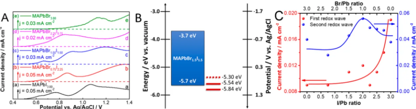
RESULTS AND DISCUSSIONSelective Hole Injection via Electrochemistry.On the basis of the electrochemical protocols outlined in our previous study43 we recorded linear sweep voltammograms (LSVs) in Figure 1.(A) Linear sweep voltammograms of FTO/MAPbBrxI3−xfilms in 0.1 M Bu4NPF6/DCM electrolyte (5 mV s−1sweep rate). (B) Band diagram of MAPbBr1.5I1.5together with the peak onset of the observed Faradaic events. (C) Variation of the peak currents of thefirst two redox waves as a function of MHP composition, with solid lines to guide the eye.
Figure 2.(A) Linear sweep voltammogram of a FTO/MAPbBr1.5I1.5film in 0.1 M Bu4NPF6/DCM electrolyte (5 mV s−1sweep rate) plotted together with the absorbance change at 470 nm. Region#1 is where hole trapping occurs, and region#2 is where hole injection to the valence band occurs. (B) UV−vis spectra of FTO/MAPbBr1.5I1.5films during potentiostatic treatment at 0.9 V vs Ag/AgCl. (C) XRD patterns of thick FTO/
MAPbBrxI3−xelectrodes before and after potentiostatic treatment at 0.9 V vs Ag/AgCl in 0.1 M Bu4NPF6/DCM electrolyte. PC and C denote pseudocubic and cubic lattice, respectively. (D) Alteration of the optically active perovskite composition as a function of passed charge during potentiostatic treatment at 0.9 V vs Ag/AgCl. The photographs show the color change of the electrode at two stages of the potentiostatic treatment.
The standard deviation was determined from measurements on three separate FTO/MAPbBr1.5I1.5electrodes.
DOI:10.1021/jacs.9b04568 J. Am. Chem. Soc.XXXX, XXX, XXX−XXX B
0.1 M Bu4NPF6 dichloromethane (DCM) electrolyte for various MHPfilms. The LSVs show a composition dependency in the position (and magnitude) of the distinct oxidation waves (Figure 1A, Figure S1, andTable S1). Considering the redox potential of halide oxidation in lead halides43 and solution phase (i.e., bromide (+1.26 V) and iodide (+0.86 V) oxidation in this medium (Figure S2)), the more positive events on the LSV scans can be assigned to these reactions (Figure 1A and Figure S1). The MHPfilms are stable below these potentials, so thefirst two waves can be attributed to the electrochemistry of the intact MHP layers. These oxidation waves show a gradual shift to more positive potentials with increasing bromide content (Table S1), as one would expect from their increased stability in the series. We can attribute the oxidation wave in the region #1 to the trapping of holes and the subsequent movement of iodide ions in the lattice in these materials, as shown by electrochemical impedance spectrosco- py (Figure S3). Note that these states barely exist in the case of MAPbBr3. The position of the #2 oxidation wave at higher potential matches the respective valence band edge position (Figure 1B) and corresponds to hole injection into the perovskite structure (i.e., to the valence band). From the magnitude of the current density related to process #1 it is apparent that all MHP phases show decreased trap state density compared to the pure MAPbI3 phase (Figure 1C).
Notably, the rate (i.e., the current density) of process#2 peaks at approximately equimolar Br/I ratio (Figure 1C).
Selective Expulsion of Iodide from MAPbBr1.5I1.5
Films.Spectroelectrochemistry was used to track the spectral changes following the hole injection into MAPbBr1.5I1.5films.
During the initial step of hole trapping no change of the spectral features was observed (region #1 in Figure 2A). As sufficient electrochemical driving force (with increased electrode potential) is reached to induce hole injection into the valence band of MAPbBr1.5I1.5(region#2 inFigure 2A), we observe a decrease in the overall absorbance (Figure S4).
Interestingly, this process is coupled with the monotonic shift of the absorption edge (i.e., bandgap) to shorter wavelengths.
This irreversible shift in absorption edge suggests enrichment of the MHP phase with bromide-rich domains through the
selective expulsion of iodide into the solution from the perovskite lattice. The higher affinity of Pb(II) to bromide as compared to iodide in the perovskite lattice is likely to be the reason for the enrichment of bromide-rich domains after the electrochemical hole injection.12,44
Similar trends were revealed during potentiostatic experi- ments. At moderately positive potentials, where no Faradaic event occurs (i.e., 0.5 V and below), the UV−vis absorbance remains unaltered (Figure S5). However, when the applied potential was increased to 0.9 V vs Ag/AgCl, we observe a gradual decrease in absorbance, coupled with the shift in the absorption edge from 660 nm to 545 nm in 300 s. Thus, the shift in the bandgap to a higher energy region becomes evident as iodide was expelled from the perovskite lattice (Figure 2B).
During the intermediate times, the absorbance onset becomes less sharp, as residual contribution from varying degree of mixed phases is seen during the expulsion process. Once iodide expulsion from the lattice is completed, the spectrum reflects the optical features of MAPbBr3. Further anodic polarization at this potential does not change the spectrum, confirming the stability of MAPbBr3 (as predicted from the LSV traces in Figure 1A).
The effect of the iodide expulsion process on the crystal structure of the MHPfilms was monitored by X-ray diffraction (XRD) measurements (Figure 2C). A gradual shift of the MAPbBr1.5I1.5-related reflections was observed to higher 2theta values upon oxidation, which translates to the contraction of the pseudocubic perovskite crystal lattice. At an intermediate treatment time this results in the formation of MAPbBr2.6I0.4.2 Closer inspection of the pattern reveals that an additional intermediate MHP phase is also present in the films (MAPbBr2.3I0.7). The presence of multiple perovskite phases is consistent with the less sharp nature of the absorption onset seen previously on the UV−vis spectra (Figure 2B).
Interestingly, at the end of the potentiostatic treatment a slightly contracted MAPbBr3 lattice was formed, which is possibly caused by the presence of defects in the re-formed crystal lattice. Reflections from both PbI2and PbBr2phases are also present in all cases (as also deduced from X-ray photoelectron spectroscopy, XPS), however only weakly.
Figure 3.Top-down SEM images of FTO/MAPbBr1.5I1.5films at different magnifications. (A, D) Pristinefilms, (B, E)films treated at 0.9 V vs Ag/
AgCl for 30 s (until 1.3 mC cm−2charge density was passed), (C, F)films treated at 0.9 V vs Ag/AgCl for 300 s (until 3.7 mC cm−2charge density is passed).
DOI:10.1021/jacs.9b04568 J. Am. Chem. Soc.XXXX, XXX, XXX−XXX C
This signals that their formation is confined to the surface of the MHPfilms (or that their crystal domain size is rather small and not continuous) and the bulk of the material retains the perovskite crystal lattice. The XRD data strengthen the notion that the iodide expulsion process is accompanied by the dynamic re-formation of the perovskite lattice, and not just the destruction and ultimate dissolution of the material are achieved.45 In situ Raman spectroelectrochemistry (Figures S6−S8) further confirmed the formation of iodide- and bromide-rich domains as thefirst step of the iodide expulsion process. As the applied electrochemical bias was increased (until the point where iodide migration starts in the films), a broadfluorescence signal was observed (Figure S7B). This can be attributed to the formation of domains capable of absorbing (and emitting) the exciting laser light (λ= 780 nm).
To quantify the electrochemically induced iodide expulsion process, we determined the composition of the films from Tauc plots using the recorded UV−vis spectra and a previously obtained bandgap−composition relationship (Figure S9). The Pb/halide composition of thefilm was found to be dependent on the net charge injected into the MAPbBr1.5I1.5films (Figure 2D). To minimize the contribution of charging/discharging of the electrical double layer, a preconditioning step (at 0.5 V vs Ag/AgCl for 30 s,Figure S10) was employed, when calculating the charge during the potentiostatic treatment. The effect of electrochemical iodide expulsion was also visually observed, as the dark appearance of the MAPbBr1.5I1.5films slowly changed, ultimately resulting in a yellow-colored bromide-richfilm when the process was completed (Figure 2D).
Morphological Changes. With the expulsion of iodide upon hole injection, one would expect morphological changes
associated with the spectral changes. Top-down SEM images were recorded to visualize these changes of the MAPbBr1.5I1.5 films (Figure 3). The alteration of the initially smooth surface to a rougher one was observed with increasing time of the electrochemical biasing. This process is accompanied by the formation of voids in thefilms. Both the size of the voids and their number increase with the injected charge into the MAPbBr1.5I1.5film (31±15 nm at 1.3 mC cm−2and 116±31 nm at 3.7 mC cm−2injected charge density). The voids in the film further confirm the loss of iodide as the crystal structure re-forms. The evolution of the morphology suggests that MAPbBr1.5I1.5 continuously undergoes structural changes, ultimately yielding the MAPbBr3structure.
Compositional Analysis. Since the electrode/electrolyte interface plays a pivotal role in the iodide expulsion process, XPS measurements were carried out to probe the alteration of the surface composition of the MAPbBr1.5I1.5films during the potentiostatic treatment (Table S2). The surface of the MAPbBr1.5I1.5 film was enriched in iodide even before electrochemical treatment. In the intermediate step of the electrochemical treatment we continue to see this excess iodide that remains at the surface, but with a concomitant decrease in the bromide content. This is indicative of the MAPbBr1.5I1.5 surface becoming rich in PbI2. This trend signals that iodide constantly migrates to the surface of the film, before getting expelled to the solution. Bromide remains preferentially in the deeper regions of the film. As the electrochemical treatment process was completed, a decrease of PbI2on the surface of the films was observed. Thefinal depletion of iodide on the surface signals that the composition of the perovskite phase located on Figure 4.Time-resolved transient absorption spectra recorded following 387 nm laser pulse excitation (4μJ cm−2) of (A) pristine FTO/MAPbBr3 films, (B) pristine FTO/MAPbBr1.5I1.5films, and (C) FTO/MAPbBr1.5I1.5films after potentiostatic treatment at 0.9 V vs Ag/AgCl for 300 s under vacuum. (D) Recovery profiles of the perovskitefilms monitored at their ground state bleach maxima and the corresponding biexponentialfits.
DOI:10.1021/jacs.9b04568 J. Am. Chem. Soc.XXXX, XXX, XXX−XXX D
the potentiostatic treatments there is still remnant iodide left in thefilms. A plausible explanation for this is the formation of a PbI2 intermediate during the expulsion process (see also additional absorbance at 450−500 nm inFigure 2B compared toFigure S6A). A detailed discussion on the cross-correlation of the determined compositions can be found in theSI.
Excited State Dynamics.We also probed the excited state behavior of MAPbBr1.5I1.5 films to see the effect of iodide expulsion on the charge carrier recombination dynamics. The transient absorption spectra of MHP films were recorded before and after electrochemical treatment (holding the electrode at +0.9 V vs Ag/AgCl), as well as for a pure MAPbBr3 film (Figure 4A). The intact MAPbBr1.5I1.5 films showed an intense bleach signal centered at 640 nm and recovered within 1.6 ns after excitation (Figure 4B). This transient behavior has been discussed in detail elsewhere.12,41 After the electrochemical treatment, a blue-shifted ground state bleach was seen, in accordance with the expulsion of iodide from the perovskite lattice (Figure 4C). Specifically, the maximum of this bleach signal appears at shorter wavelengths (540 nm), which is close to the ground state bleach maximum (530 nm) of pure MAPbBr3 films (Figure 4A). Furthermore, the maximum intensity of the bleach signal of the MHPfilm after the electrochemical treatment is decreased in accordance with the decreased absorbance following the iodide expulsion.
Figure 4D compares the recovery kinetics of the bleach signal of MAPbBr1.5I1.5films before and after electrochemical treatment and the pristine MAPbBr3film. The charge carrier lifetime of the two untreated perovskitefilms are similar (571
± 68 ps in MAPbBr3 and 381 ± 28 ps in untreated MAPbBr1.5I1.5). After the electrochemical treatment (following complete iodide expulsion from the MAPbBr1.5I1.5 film) the recovery becomes faster (16±8 ps). As the iodide is expelled, we expect to see an increase in the number of defect sites. A significant change in the surface morphology seen on the SEM images further supports this notion. These defect sites are responsible for the observed enhancement in the recombina- tion of charge carriers.
Mechanistic Insights. The results presented above highlight the effect of hole injection on the compositional, structural, and morphological features of MAPbBr1.5I1.5films.
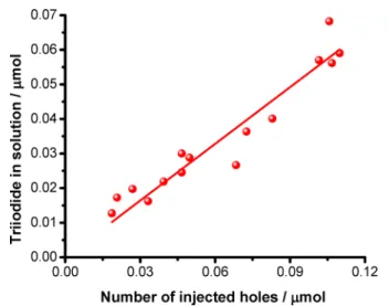
However, the mechanism behind iodide expulsion remains an intriguing question. To elucidate the form in which iodide leaves the lattice (I− or I2), we recorded the UV−vis absorbance spectra of the electrolyte after various amounts of charge injection into the MAPbBr1.5I1.5films. We found that the predominant species formed in the solution phase is I3−, which points toward either the direct expulsion of I3−from the layer or the parallel I−and I2injection to the solution. In terms of the net redox reaction (eq 1), the trapping of two holes on the iodide sites of four perovskite units results in the formation of one I2 molecule. To check the validity of the proposed
found between the number of injected holes and the amount of I3−in the solution. Furthermore, the slope of thefitted line was 0.55 ± 0.02, which is in close agreement with the proposed reaction (i.e., 0.5 theoretical value, meaning a 10% deviation).
At the same time, during the re-formation of the structure after hole trapping and iodide oxidation, partial dissolution of the MAPbBr1.5I1.5structure also occurs (eq 2), thus leaching I− ions into the solution, which can form the triiodide complex with I2. Note that without electrochemical bias the films are stable within the time frame of the experiments; therefore physical dissolution cannot account for the presence of I−ions in the solution. Overall, these three processes together can explain the absence of I2 species in the solution and the exclusive presence of I3−.
To gain further insight into the mechanistic features, we carried out first-principles calculations employing a hybrid DFT+SOC computational approach; see SI for details. We focus on the nature of hole traps in MAPbI3, MAPbBr3, and MAPbBrxI3−x. The defect chemistry of lead halide perovskites is dominated by lead vacancies (VPb) and interstitial halides (Xi, X = I, Br),46,47which are stable defects that can trap holes through the (−2/−) and (−/0) transitions, respectively, both in MAPbI3 and MAPbBr3 (see Figure 6A). Despite the apparently different nature, the two types of defects are quite similar, being related to the presence of undercoordinated iodine atoms in the lattice, either because of a lack of lead (VPb) or added halide (Xi).
In MAPbI3, the (−/0) transition of Ii, corresponding to hole trapping at negatively charged interstitial iodine (Ii−→Ii0), is calculated at 0.29 eV above the valence band (VB), similar to the (−2/−) transition of VPb, calculated at 0.13 eV. The calculated transition energies nicely match the energy differ- ence measured by voltammetry for traps and VB oxidation in MAPbI3, 0.62 and 0.77 V vs Ag/AgCl, respectively; seeTable S1 andFigure 1A. In MAPbBr3a similar picture is predicted, although both transition levels are somehow shallower, Figure 5.Dependence of the formed triiodide amount in the solution phase (0.1 M Bu4NPF6in DCM) on the amount of injected charge to thick MAPbBr1.5I1.5films. Thefilms were subjected to potentiostatic treatment at 0.9 V vs Ag/AgCl, while the UV−vis absorbance of the electrolyte was measured. The triiodide concentration was determined from the absorption peak located at 364 nm.
DOI:10.1021/jacs.9b04568 J. Am. Chem. Soc.XXXX, XXX, XXX−XXX E
consistent with the merging of the trap oxidation peaks into the signal of VB oxidation; see Table S1 and Figure 1A.
Interestingly, in the case of MAPbBrxI3−x we predict substitution of interstitial iodide by bromide to be favored by 0.1 eV compared to substitution of lattice iodide. This behavior means that in the presence of interstitial iodide in MAPbI3Br incorporation will preferentially lead to a mixed I/
Br interstitial defect (Figure 6A, middle row), whose (−/0) transition energy level is calculated at 0.03 eV above the VB.
Thus, while the VB edge becomes significantly more positive upon increasing Br incorporation into the lattice (0.77→1.15 V vs Ag/AgCl), oxidation of the trap states only slightly drifts toward more positive potentials, remaining always close to its value in MAPbI3(0.62→ 0.67 V vs Ag/AgCl, seeTable S1 and Figure 1A). The overall picture extracted from theory is thus fully consistent with the experimental results and suggests that the energetics of trap states are mainly contributed by iodine even in mixed I/Br perovskites, whereby the (−/0) transition of the mixed I/Br interstitial defect remains almost constant while the VB deepens (Figure 6B).
Most notably, experiments clearly indicate that hole injection into the trap states is not sufficient to promote iodide expulsion from the lattice (seeFigure 2A). Nevertheless, traps arefilled at less positive potentials than the VB; thus they are filled before iodide expulsion is observed and likely contribute to this reaction. In particular, defects are known to promote ion migration in perovskites (and in general in ionic conductors), and significant ion migration has to take place upon hole injection to lead to iodide expulsion. Based on this analysis, a possible mechanism can be sketched as follows:
+ → + +
+
+ +
h
4MAPbBr I 2 2MAPbBr 2PbI 2MA
I overall redox process
1.5 1.5 3 2
2 (1)
→ + + ++ −
2MAPbBr I MAPbBr PbI MA I
partial dissolution
1.5 1.5 3 2
(2) + →
− +
h
Ii Ii0 trap filling (3)
+ h+→ h+
VB 1 @VB VB oxidation (4)
+ →
+ +
h
1 @VB Ii0 Ii trap oxidation (5)
+ → +
+ − +
Ii I I2 VI iodine formation (6)
+ → +
+ − − +
Ii 2I I3 2VI triiodide formation (6a) where Ii−, Ii0, and Ii+denote a negatively charged, a neutral, and a positively charged interstitial iodine, I−is a lattice iodide, and VI+is an iodine vacancy.
Equations 3 and 4 correspond to the sequential hole injection into the traps and the VB. Under prolonged electrochemical bias, a hole is transferred from the VB to the filled trap, leading to oxidation of Ii0to Ii+,eq 5. Ii+has a trimer structure48typical of I3−.Equation 6corresponds to the attack of Ii+ to lattice iodide (I−) to generate molecular iodine (I2) and an iodine vacancy, VI+. Alternatively, ineq 6aIi+abstracts two iodine atoms from the lattice to exit in the form of I3−. In eq 6 I2can be formed either in the bulk or at surfaces/grain boundaries. Molecular iodine is unstable in the lattice;49 if formed in the bulk, I2 thus tends to migrate to the surface, where it can be easily abstracted to the solution. The reaction ineq 6is calculated to be energetically unfavorable by 0.39 eV when Ii+ and VI+ are bulk defects and I2 is formed as a gas phase molecule (neglecting thermal corrections to enthalpy and entropy). I2 surface stabilization and its subsequent solvation with consequent energetic and entropic gain, however, provide energetically favorable pathways for iodide expulsion.
■
CONCLUSIONSAs noted earlier, the halide ions within the perovskite exhibit mobility with relatively low activation energy.50 When subjected to steady state light irradiation, the single-anion- containing phases in mixed halides segregate. The diffusion length of the charge carriers is an important parameter that dictates the phase segregation in MHP films.21 Cathode luminescence studies have shown that iodide ions selectively accumulate near the grain boundaries.33 In contrast to Figure 6.(A) Structures and (B) transition energies of stable hole-trapping defects in MAPbI3, MAPbBr3, and MAPbBrxI3−x. The zero of the energy scale is set to the MAPbI3VB maximum.
DOI:10.1021/jacs.9b04568 J. Am. Chem. Soc.XXXX, XXX, XXX−XXX F
photoirradiation (where equal amounts of electrons and holes are formed), we have employed selective injection of holes through electrochemical treatment to deconvolute the complex effect of different charge carriers. While in single-anion- containing perovskites hole injection causes the direct degradation of the structure, the situation is more complex for MHPs. The trapped holes at the iodide sitesfirst cause the phase segregation and subsequently the disintegration of the crystal structure, through intermediate crystal phases (Scheme 1). The blue shift in the absorption feature is indicative of the loss of methylammonium ion as the accomplice of iodine (or triiodide) during their expulsion. Overall, the electrochemically induced phase segregation with ultimate expulsion of iodine provides new evidence of hole trapping as the driving force for the halide ion mobility. What is further important, simple electrochemical measurements can provide a new tool to assess the stability of different MHPs in a rapid way, thus avoiding the need of long-term initial testing during materials screening.
■
ASSOCIATED CONTENT*S Supporting Information
The Supporting Information is available free of charge on the ACS Publications website at DOI:10.1021/jacs.9b04568.
(Complete experimental section (including used materi- als, characterization methods, electrode preparation), additional electrochemical measurements (LSVs, EIS, in situ Raman spectroelectrochemistry), complete compo- sitional analysis (XPS, EDX, ICP-OES, IC results) together with discussion and lifetime calculationsPDF)
■
AUTHOR INFORMATION Corresponding Authors*pkamat@nd.edu; Twitter: @KamatLab
*janaky@chem.u-szeged.hu; Twitter @Janakylab ORCID
Gergely F. Samu: 0000-0002-3239-9154
Filippo De Angelis: 0000-0003-3833-1975
Daniele Meggiolaro:0000-0001-9717-133X
Prashant V. Kamat: 0000-0002-2465-6819
Csaba Janáky: 0000-0001-5965-5173 Notes
The authors declare no competingfinancial interest.
■
ACKNOWLEDGMENTSThe authors thank the Notre Dame Integrated Imaging Facility and Dr. Tatyana Orlova for taking the SEM images. We thank Dr. Allen G. Oliver for recording the XRD patterns and the valuable discussion. We thank the Center for Environmental
Science and Technology at the University of Notre Dame for the use of their instrumentation and the help of Jon Loftus and Jeffrey DuBose with the ICP-OES and ion chromatography measurements. We are grateful for the help of Sylwia Ptasinska and Pitambar Sapkota with the XPS measurements and the evaluation, as well as to Rebecca A. Scheidt for the support in the TAS measurements. P.V.K. acknowledges support by the Division of Chemical Sciences, Geosciences, and Biosciences, Office of Basic Energy Sciences of the U.S. Department of Energy (award DE-FC02- 04ER15533). This collaborative research received funding from the European Research Council (ERC) under the EU’s Horizon 2020 research and innovation program (G.F.S., A.B., and C.J., grant agreement No. 716539). ELI-ALPS is supported by the EU and cofinanced by the European Regional Development Fund (GOP-1.1.1-12/B-2012-000, GINOP-2.3.6-15-2015-00001).
This is contribution number NDRL No. 5250 from the Notre Dame Radiation Laboratory. F.D.A. acknowledges support from the Italian “Ministero per l’Università e la Ricerca Scientifica e Tecnologica”, MIUR (Rome, Italy), and the University of Perugia, under the “Dipartimenti di Eccellenza 2018-2022” (grant AMIS) and from the European Union’s Horizon 2020 research and innovation program, under grant agreement No. 764047.
■
(1) McMeekin, D. P.; Sadoughi, G.; Rehman, W.; Eperon, G. E.;REFERENCES Saliba, M.; Horantner, M. T.; Haghighirad, A.; Sakai, N.; Korte, L.;Rech, B.; Johnston, M. B.; Herz, L. M.; Snaith, H. J. A Mixed-Cation Lead Mixed-Halide Perovskite Absorber for Tandem Solar Cells.
Science2016,351, 151−155.
(2) Noh, J. H.; Im, S. H.; Heo, J. H.; Mandal, T. N.; Seok, S. Il.
Chemical Management for Colorful, Efficient, and Stable Inorganic− Organic Hybrid Nanostructured Solar Cells.Nano Lett.2013,13(4), 1764−1769.
(3) Bush, K. A.; Palmstrom, A. F.; Yu, Z. J.; Boccard, M.;
Cheacharoen, R.; Mailoa, J. P.; McMeekin, D. P.; Hoye, R. L. Z.;
Bailie, C. D.; Leijtens, T.; Peters, I. M.; Minichetti, M. C.; Rolston, N.;
Prasanna, R.; Sofia, S.; Harwood, D.; Ma, W.; Moghadam, F.; Snaith, H. J.; Buonassisi, T.; Holman, Z. C.; Bent, S. F.; McGehee, M. D.
23.6%-Efficient Monolithic Perovskite/Silicon Tandem Solar Cells with Improved Stability.Nat. Energy2017,2, 17009.
(4) Zhao, D.; Wang, C.; Song, Z.; Yu, Y.; Chen, C.; Zhao, X.; Zhu, K.; Yan, Y. Four-Terminal All-Perovskite Tandem Solar Cells Achieving Power Conversion Efficiencies Exceeding 23%.ACS Energy Lett.2018,3, 305−306.
(5) Beal, R. E.; Slotcavage, D. J.; Leijtens, T.; Bowring, A. R.; Belisle, R. A.; Nguyen, W. H.; Burkhard, G. F.; Hoke, E. T.; McGehee, M. D.
Cesium Lead Halide Perovskites with Improved Stability for Tandem Solar Cells.J. Phys. Chem. Lett.2016,7, 746−751.
(6) Eperon, G. E.; Leijtens, T.; Bush, K. A.; Prasanna, R.; Green, T.;
Wang, J. T.-W.; McMeekin, D. P.; Volonakis, G.; Milot, R. L.; May,
DOI:10.1021/jacs.9b04568 J. Am. Chem. Soc.XXXX, XXX, XXX−XXX G
R.; Palmstrom, A.; Slotcavage, D. J.; Belisle, R. A.; Patel, J. B.; Parrott, E. S.; Sutton, R. J.; Ma, W.; Moghadam, F.; Conings, B.; Babayigit, A.;
Boyen, H.; Bent, S.; Giustino, F.; Herz, L. M.; Johnston, M. B.;
McGehee, M. D.; Snaith, H. J. Perovskite-Perovskite Tandem Photovoltaics with Optimized Band Gaps. Science2016,354, 861−
865.
(7) Leijtens, T.; Bush, K. A.; Prasanna, R.; McGehee, M. D.
Opportunities and Challenges for Tandem Solar Cells Using Metal Halide Perovskite Semiconductors.Nat. Energy2018,3, 828−838.
(8) Hoffman, J. B.; Schleper, A. L.; Kamat, P. V. Transformation of Sintered CsPbBr3 Nanocrystals to Cubic CsPbI3 and Gradient CsPbBrxI3−xthrough Halide Exchange.J. Am. Chem. Soc.2016,138, 8603−8611.
(9) Zhou, C.; Ou, Q.; Chen, W.; Gan, Z.; Wang, J.; Bao, Q.; Wen, X.; Jia, B. Illumination-Induced Halide Segregation in Gradient Bandgap Mixed-Halide Perovskite Nanoplatelets. Adv. Opt. Mater.
2018,6, 1801107.
(10) Ravi, V. K.; Scheidt, R. A.; Nag, A.; Kuno, M.; Kamat, P. V. To Exchange or Not to Exchange. Suppressing Anion Exchange in Cesium Lead Halide Perovskites with PbSO4−Oleate Capping.ACS Energy Lett.2018,3, 1049−1055.
(11) Pan, D.; Fu, Y.; Chen, J.; Czech, K. J.; Wright, J. C.; Jin, S.
Visualization and Studies of Ion-Diffusion Kinetics in Cesium Lead Bromide Perovskite Nanowires.Nano Lett.2018,18, 1807−1813.
(12) Yoon, S. J.; Kuno, M.; Kamat, P. V. Shift Happens. How Halide Ion Defects Influence Photoinduced Segregation in Mixed Halide Perovskites.ACS Energy Lett.2017,2, 1507−1514.
(13) Belisle, R. A.; Bush, K. A.; Bertoluzzi, L.; Gold-Parker, A.;
Toney, M. F.; McGehee, M. D. Impact of Surfaces on Photoinduced Halide Segregation in Mixed-Halide Perovskites. ACS Energy Lett.
2018,3, 2694−2700.
(14) Duong, T.; Mulmudi, H. K.; Wu, Y.; Fu, X.; Shen, H.; Peng, J.;
Wu, N.; Nguyen, H. T.; Macdonald, D.; Lockrey, M.; White, T. P.;
Weber, K.; Catchpole, K. Light and Electrically Induced Phase Segregation and Its Impact on the Stability of Quadruple Cation High Bandgap Perovskite Solar Cells.ACS Appl. Mater. Interfaces2017,9, 26859−26866.
(15) Braly, I. L.; Stoddard, R. J.; Rajagopal, A.; Uhl, A. R.; Katahara, J. K.; Jen, A. K.-Y.; Hillhouse, H. W. Current-Induced Phase Segregation in Mixed Halide Hybrid Perovskites and Its Impact on Two-Terminal Tandem Solar Cell Design.ACS Energy Lett.2017,2, 1841−1847.
(16) Lin, Y.; Chen, B.; Fang, Y.; Zhao, J.; Bao, C.; Yu, Z.; Deng, Y.;
Rudd, P. N.; Yan, Y.; Yuan, Y.; Huang, J. Excess Charge-Carrier Induced Instability of Hybrid Perovskites. Nat. Commun. 2018, 9, 4981.
(17) Ruf, F.; Rietz, P.; Aygüler, M. F.; Kelz, I.; Docampo, P.; Kalt, H.; Hetterich, M. The Bandgap as a Moving Target: Reversible Bandgap Instabilities in Multiple-Cation Mixed-Halide Perovskite Solar Cells.ACS Energy Lett.2018,3, 2995−3001.
(18) Samu, G. F.; Janáky, C.; Kamat, P. V. A Victim of Halide Ion Segregation. How Light Soaking Affects Solar Cell Performance of Mixed Halide Lead Perovskites. ACS Energy Lett. 2017, 2, 1860− 1861.
(19) Braly, I. L.; Stoddard, R. J.; Rajagopal, A.; Uhl, A. R.; Katahara, J. K.; Jen, A. K.-Y.; Hillhouse, H. W. Current-Induced Phase Segregation in Mixed Halide Hybrid Perovskites and Its Impact on Two-Terminal Tandem Solar Cell Design.ACS Energy Lett.2017,2, 1841−1847.
(20) Tang, X.; van den Berg, M.; Gu, E.; Horneber, A.; Matt, G. J.;
Osvet, A.; Meixner, A. J.; Zhang, D.; Brabec, C. J. Local Observation of Phase Segregation in Mixed-Halide Perovskite.Nano Lett.2018,18, 2172−2178.
(21) Draguta, S.; Sharia, O.; Yoon, S. J.; Brennan, M. C.; Morozov, Y. V.; Manser, J. S.; Kamat, P. V.; Schneider, W. F.; Kuno, M.
Rationalizing the Light-Induced Phase Separation of Mixed Halide Organic−inorganic Perovskites.Nat. Commun.2017,8, 200.
(22) Gualdrón-Reyes, A. F.; Yoon, S. J.; Barea, E. M.; Agouram, S.;
Muñoz-Sanjosé, V.; Meléndez, Á. M.; Niño-Gómez, M. E.; Mora-
Seró, I. Controlling the Phase Segregation in Mixed Halide Perovskites through Nanocrystal Size. ACS Energy Lett. 2019, 4, 54−62.
(23) Mao, W.; Hall, C. R.; Chesman, A. S. R.; Forsyth, C.; Cheng, Y.-B.; Duffy, N. W.; Smith, T. A.; Bach, U. Visualizing Phase Segregation in Mixed-Halide Perovskite Single Crystals.Angew. Chem., Int. Ed.2019,58, 2893−2898.
(24) Hu, M.; Bi, C.; Yuan, Y.; Bai, Y.; Huang, J. Stabilized Wide Bandgap MAPbBrxI3‑x Perovskite by Enhanced Grain Size and Improved Crystallinity.Adv. Sci.2016,3, 1500301.
(25) Bischak, C. G.; Wong, A. B.; Lin, E.; Limmer, D. T.; Yang, P.;
Ginsberg, N. S. Tunable Polaron Distortions Control the Extent of Halide Demixing in Lead Halide Perovskites. J. Phys. Chem. Lett.
2018,9, 3998−4005.
(26) Oranskaia, A.; Yin, J.; Bakr, O. M.; Brédas, J.-L.; Mohammed, O. F. Halogen Migration in Hybrid Perovskites: The Organic Cation Matters.J. Phys. Chem. Lett.2018,9, 5474−5480.
(27) Knight, A. J.; Wright, A. D.; Patel, J. B.; McMeekin, D. P.;
Snaith, H. J.; Johnston, M. B.; Herz, L. M. Electronic Traps and Phase Segregation in Lead Mixed-Halide Perovskite.ACS Energy Lett.2019, 4, 75−84.
(28) Barker, A. J.; Sadhanala, A.; Deschler, F.; Gandini, M.;
Senanayak, S. P.; Pearce, P. M.; Mosconi, E.; Pearson, A. J.; Wu, Y.;
Srimath Kandada, A. R.; Leijtens, T.; De Angelis, F.; Dutton, S. E.;
Petrozza, A.; Friend, R. H. Defect-Assisted Photoinduced Halide Segregation in Mixed-Halide Perovskite Thin Films.ACS Energy Lett.
2017,2, 1416−1424.
(29) Yang, X.; Yan, X.; Wang, W.; Zhu, X.; Li, H.; Ma, W.; Sheng, C.
Light Induced Metastable Modification of Optical Properties in CH3NH3PbI3‑xBrx Perovskite Films: Two-Step Mechanism. Org.
Electron.2016,34, 79−83.
(30) Hoke, E. T.; Slotcavage, D. J.; Dohner, E. R.; Bowring, A. R.;
Karunadasa, H. I.; McGehee, M. D. Reversible Photo-Induced Trap Formation in Mixed-Halide Hybrid Perovskites for Photovoltaics.
Chem. Sci.2015,6, 613−617.
(31) Slotcavage, D. J.; Karunadasa, H. I.; McGehee, M. D. Light- Induced Phase Segregation in Halide-Perovskite Absorbers. ACS Energy Lett.2016,1, 1199−1205.
(32) Ruth, A.; Brennan, M. C.; Draguta, S.; Morozov, Y. V.;
Zhukovskyi, M.; Janko, B.; Zapol, P.; Kuno, M. Vacancy-Mediated Anion Photosegregation Kinetics in Mixed Halide Hybrid Perov- skites: Coupled Kinetic Monte Carlo and Optical Measurements.ACS Energy Lett.2018,3, 2321−2328.
(33) Bischak, C. G.; Hetherington, C. L.; Wu, H.; Aloni, S.;
Ogletree, D. F.; Limmer, D. T.; Ginsberg, N. S. Origin of Reversible Photoinduced Phase Separation in Hybrid Perovskites. Nano Lett.
2017,17, 1028−1033.
(34) Miyata, K.; Meggiolaro, D.; Trinh, M. T.; Joshi, P. P.; Mosconi, E.; Jones, S. C.; De Angelis, F.; Zhu, X.-Y. Large Polarons in Lead Halide Perovskites.Sci. Adv.2017,3, No. e1701217.
(35) Stranks, S. D.; Eperon, G. E.; Grancini, G.; Menelaou, C.;
Alcocer, M. J. P.; Leijtens, T.; Herz, L. M.; Petrozza, A.; Snaith, H. J.
Electron-Hole Diffusion Lengths Exceeding 1 Micrometer in an Organometal Trihalide Perovskite Absorber.Science2013,342, 341−
344.
(36) de Quilettes, D. W.; Vorpahl, S. M.; Stranks, S. D.; Nagaoka, H.; Eperon, G. E.; Ziffer, M. E.; Snaith, H. J.; Ginger, D. S. Impact of Microstructure on Local Carrier Lifetime in Perovskite Solar Cells.
Science2015,348, 683−686.
(37) Xing, G.; Mathews, N.; Sun, S.; Lim, S. S.; Lam, Y. M.; Gratzel, M.; Mhaisalkar, S.; Sum, T. C. Long-Range Balanced Electron- and Hole-Transport Lengths in Organic-Inorganic CH3NH3PbI3.Science 2013,342, 344−347.
(38) Eames, C.; Frost, J. M.; Barnes, P. R. F.; O’Regan, B. C.; Walsh, A.; Islam, M. S. Ionic Transport in Hybrid Lead Iodide Perovskite Solar Cells.Nat. Commun.2015,6, 7497.
(39) Kim, G. Y.; Senocrate, A.; Yang, T.-Y.; Gregori, G.; Grätzel, M.;
Maier, J. Large Tunable Photoeffect on Ion Conduction in Halide
DOI:10.1021/jacs.9b04568 J. Am. Chem. Soc.XXXX, XXX, XXX−XXX H
(43) Samu, G. F.; Scheidt, R. A.; Kamat, P. V.; Janáky, C.− Electrochemistry and Spectroelectrochemistry of Lead Halide Perov- skite Films: Materials Science Aspects and Boundary Conditions.
Chem. Mater.2018,30, 561−569.
(44) Yoon, S. J.; Stamplecoskie, K. G.; Kamat, P. V. How Lead Halide Complex Chemistry Dictates the Composition of Mixed Halide Perovskites.J. Phys. Chem. Lett.2016,7, 1368−1373.
(45) Manser, J. S.; Saidaminov, M. I.; Christians, J. A.; Bakr, O. M.;
Kamat, P. V. Making and Breaking of Lead Halide Perovskites. Acc.
Chem. Res.2016,49, 330−338.
(46) Meggiolaro, D.; De Angelis, F. First-Principles Modeling of Defects in Lead Halide Perovskites: Best Practices and Open Issues.
ACS Energy Lett.2018,3, 2206−2222.
(47) Meggiolaro, D.; Motti, S. G.; Mosconi, E.; Barker, A. J.; Ball, J.;
Andrea Riccardo Perini, C.; Deschler, F.; Petrozza, A.; De Angelis, F.
Iodine Chemistry Determines the Defect Tolerance of Lead-Halide Perovskites.Energy Environ. Sci.2018,11, 702−713.
(48) Du, M.-H. Density Functional Calculations of Native Defects in CH3NH3PbI3: Effects of Spin−Orbit Coupling and Self-Interaction Error.J. Phys. Chem. Lett.2015,6, 1461−1466.
(49) Meggiolaro, D.; Mosconi, E.; De Angelis, F. Modeling the Interaction of Molecular Iodine with MAPbI3: A Probe of Lead- Halide Perovskites Defect Chemistry.ACS Energy Lett.2018,3, 447− 451.
(50) Yuan, Y.; Huang, J. Ion Migration in Organometal Trihalide Perovskite and Its Impact on Photovoltaic Efficiency and Stability.
Acc. Chem. Res.2016,49, 286−293.
DOI:10.1021/jacs.9b04568 J. Am. Chem. Soc.XXXX, XXX, XXX−XXX I