Light-field-driven current control in solids with pJ-level laser pulses at 80 MHz repetition rate
Václav Hanus,
1,* Viktória Csajbók,
1Zsuzsanna Pápa,
1,2Judit Budai,
2Zsuzsanna Márton,
2Gellért Zsolt Kiss,
1Péter Sándor,
1Pallabi Paul,
3Adriana Szeghalmi,
3,4Zilong Wang,
5Boris Bergues,
5,6Matthias F. Kling,
5,6György Molnár,
7János Volk,
7 ANDPéter Dombi
1,21Wigner Research Centre for Physics, Konkoly-Thege M. u. 29-33, Budapest 1121, Hungary
2ELI-ALPS, ELI-HU Non-Profit Ltd., Wolfgang Sandner u. 3, Szeged 6728, Hungary
3Institute of Applied Physics, Abbe Center of Photonics, Friedrich Schiller University Jena, Albert-Einstein-Str. 15, 07745 Jena, Germany
4Fraunhofer Institute for Applied Optics and Precision Engineering, Centre of Excellence in Photonics, Albert-Einstein-Str. 7, 07745 Jena, Germany
5Physics Department, Ludwig-Maximilians-Universität Munich, Am Coulombwall 1, 85748 Garching, Germany
6Max Planck Institute of Quantum Optics, Hans-Kopfermann-Str. 1, 85748 Garching, Germany
7Centre for Energy Research, Institute of Technical Physics and Materials Science, Konkoly-Thege M. u. 29-33, Budapest 1121, Hungary
*Corresponding author: hanus.vaclav@wigner.hu
Received 20 January 2021; revised 27 March 2021; accepted 27 March 2021 (Doc. ID 420360); published 19 April 2021
Future PHz electronic devices may be able to perform operations on few-femtosecond time-scales. Such devices are based on the ability to control currents induced by intense few-cycle laser pulses. Investigations of this control scheme have been based on complex, amplified laser systems, typically delivering mJ or sub-mJ-level laser pulses, limiting the achievable clock rate to the kHz regime. Here, we demonstrate transient metallization and lightwave-driven current control with 300-pJ laser pulses at 80 MHz repetition rate in dielectric media (HfO2and fused silica), and the wide- bandgap semiconductor GaN. We determine the field strength dependence of optically induced currents in these media.
Supported by a theoretical model, we show scaling behaviors that will be instrumental in the construction of PHz electronic devices. © 2021 Optical Society of America under the terms of theOSA Open Access Publishing Agreement
https://doi.org/10.1364/OPTICA.420360
1. INTRODUCTION
It is a substantial challenge to construct solid-state photonic devices capable of performing operations on the timescale of the optical cycles of visible or infrared lightwaves. Such devices are highly desired for petahertz (PHz) electronics applications [1,2] or to construct new diagnostic instruments for few-cycle laser pulses.
A PHz electronics device can be based on the effect of transient metallization of wide-bandgap materials or, alternatively, on the ultrafast electron transport across vacuum nanojunctions in field- enhancing nanoarchitectures [3–5]. The effect of metallization has been already demonstrated in dielectrics [6–8] such as SiO2, CaF2, or Al2O3, and semiconductors [9,10] such as GaN or graphene [11]. Unlike nanojunctions, it has the potential to circumvent technological challenges such as reliable nanojunction fabrication or the requirement of off-resonant plasmonic nanostructures [12] to support PHz bandwidth. Few-cycle laser-pulse-induced femtosecond transient metallization has proven to be a promis- ing phenomenon, thanks to its unprecedentedly fast electronic response [13]. Unlike the competitive phenomenon of current generation via interference of two quantum pathways in the tran- sitions between the valence and conduction band [14–16], the transient metallization is considerednotto produce real carriers in the conduction band [2,13], which is advantageous in terms of a
large supporting bandwidth and low dissipation of the deposited energy. Optically induced currents in materials, however, are limited to a narrow parameter range of the laser pulses, since strict requirements must be met with respect to intensity and pulse length. Even for few-cycle laser pulses where the damage threshold is increased with respect to longer pulses, the peak intensity is clamped by optical damage phenomena. This limits the applicable intensity range to a narrow domain. In spite of these limitations, first applications of the transient metallization effect have already been demonstrated in the development of carrier-envelope phase (CEP) detectors [17] or PHz waveform samplers [18]. These demonstrations also involved control of optically induced currents with the carrier-envelope phase of the laser pulses, as a hallmark for the strong-field nature of this process and its capability to support PHz bandwidths [1].
The first observation [6] indicated that the phenomenon of the transient metallization in dielectrics is limited to fields of about 1 V/Å and higher. These fields have been typically provided by mJ-class laser systems with very low,∼kHz repetition rates. The requirement of high field strength to trigger the phenomenon in dielectrics would hinder the miniaturization and mass applicability of potential devices. High-pulse-energy laser systems are bulky and
2334-2536/21/040570-07 Journal © 2021 Optical Society of America
have a low repetition rate, enabling only proof-of-principle experi- ments. An important step toward device-oriented applications was very recently made by Langeret al., where current control in GaN was demonstrated with a parametric amplifier system delivering 75 nJ pulses with a 200 kHz repetition rate [6]. Even in this case, however, the complexity of the light source seems prohibitive for future applications. The demonstration of optical current control purely in the bulk of a dielectric material with pJ-class, high-repetition-rate, oscillator-based laser pulses is thus highly desirable but still lacking.
Here, we fill this gap and report on the transient metallization and CEP-driven current control induced in a compact setup at a 80 MHz repetition rate with pJ-level pulses in GaN, HfO2, and SiO2. We demonstrate current control with a two orders of mag- nitude higher repetition rate and also a two orders of magnitude lower pulse energy compared to previous work. In addition, we prove that pure insulators can be used with nJ- and pJ-level laser pulses. We determine the field strength dependence of the optically generated currents and compare the current control phenomenon in the range of bandgaps between 3.5 and 9 eV. In addition, our results on pure insulators permit the movement of current control technology toward GHz repetition-rate femtosecond sources, a clock rate that is already competitive for ultrafast electronics applications.
2. EXPERIMENTAL SETUP FOR CURRENT CONTROL
We investigated the electric signal from different semiconductor and dielectric materials illuminated by laser pulses under ambient laboratory conditions in a simple geometry where a laser beam is focused between two gold electrodes into an active layer of material under investigation. For more details on the structure of
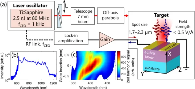
our samples, Fig.1(a) shows the geometry of the target and the illumination by few-cycle pulses. The laser beam is provided by a Ti:Sapphire laser oscillator (Venteon Laser Technologies) that provides an octave spanning spectrum [19], as shown in Fig.1(b).
The carrier-envelope offset frequency (fceo) of the pulse train can be stabilized to an arbitrary value. The oscillator emits laser pulses of 2.5 nJ at a repetition rate of 80 MHz. The duration of the pulses was characterized with a d-scan [20] yielding 5.4 fs full width at half-maximum (FWHM) of the intensity envelope. In Fig.1(c), we show the d-scan performed in situ. To ensure the shortest on-target duration, the pulses were pre-chirped with dis- persive mirrors. The pulse chirp was then fine-tuned using a pair of broadband antireflection-coated fused silica glass wedges. The maximum yield of the second harmonic signal obtained during the d-scan indicated an optimal compression of the pulses at the place of the sample. The glass wedges also allow continuously change of the CEP of the pulses impinging on the target. Details on the d-scan trace formation and reconstruction are provided in Supplement 1.
Coupling of the laser beam to the current control device is realized by tight focusing with off-axis parabolas. To achieve high on-target intensity, the beam was expanded with a telescope to a diameter of 7 mm prior to focusing. By using focusing parabolas with different focal lengths, we achieved two on-target focal spot sizes: 1.8 and 2.3µm, measured as FWHM of the intensity profile.
The focal spot sizes were characterized with a knife-edge scan.
This scheme supported intensities up to 6×10¹²W cm−2 with corresponding field strengths of up to 0.5 V/Å.
We demonstrated the high-repetition-rate current control effect in three materials: (i) epitaxially grown GaN (with a bandgap of 3.5 eV and a layer thickness of 2µm) deposited onto a sapphire plate; (ii) HfO2(with a bandgap of 5.9 eV and layer thickness of 270 nm, chosen as a compromise between fabrication difficulty
Fig. 1. (a) Scheme of the experimental setup. The laser beam from the oscillator is guided through a pair of fused silica dispersion compensation wedges.
Then the beam is expanded by a telescope to 7 mm diameter and focused onto the target by an off-axis parabola. The target is composed of a transparent substrate and an active layer of the investigated material (in case of SiO2, only the substrate is present). On top of the active layer, electrodes are patterned, forming a gap into which the laser beam is focused. Two optical waveforms (red and blue) are shown for two different (opposite) CEP values. The electrodes are connected with a pre-amplifier and lock-in amplifier. The current direction, shown with dark red arrows and dark blue arrows, oscillates as the CEP of pulses in the pulse train changes with thefceofrequency. The lock-in amplifier is referenced via a phase-locked radiofrequency link tofceoof the laser pulse train. (b) Spectrum of the laser output acquired during the phase-locked operation. (c) D-scan trace acquired during the phase-locked operation showing the second harmonic signal created in a BBO crystal (replacing the current control target) as a function of wavelength and amount of glass insertion. Zero glass insertion is calibrated to the position of maximum of the signal’s marginal integrated over the wavelength axis.
and maximization of volume of the investigated material in the sample) deposited by atomic layer deposition onto a fused silica substrate (seeSupplement 1for fabrication details); and (iii) in a bulk fused silica plate (SiO2 with a bandgap of 9.0 eV). Gold electrodes were patterned onto the substrates with electron beam lithography. The electrodes were shaped into a step-like structure so that junctions with different gap widths (0.6, 1.2, 1.7, 2.3, and 2.9µm) are accessible within the range of high-resolution linear piezo stage, as shown by the contours of the electrodes’ edges in Fig.2. Each gap has a length of 5µm providing that the laser focal spot can be well contained within one junction of a certain size.
The ultrafast current induced during the passage of the fem- tosecond pulse through the material leads to an accumulation of a charge on the attached electrodes. This accumulated charge then drives a slow current in the connected circuit that is then ampli- fied by a current preamplifier (DLPCA-200, Femto Messtechnik GmbH, Berlin, Germany). Subsequently, the signal is analyzed with a low-frequency, lock-in amplifier (SRS SR830) referenced to the carrier-envelope offset frequency, fceo. As the CEP of the pulse is related tofceoaccording toφCE=2πfceot, it is the carrier- envelope offset frequency at which we expect the change of polarity of accumulated charge on the electrodes. We chose to lock fceoto 1 kHz as the highest value of the frequency is limited by the band- width of the preamplifier, while the chosen value should be high enough to provide a stable signal. The lock-in amplifier measures the voltage,V, the output of the preamplifier can be converted to current,J, by dividing by the gain factor,G, of the preamplifier:
J =G−1V. Finally, two quantities representing the current are retrieved: in-phase component Jcos and quadrature Jsin, which represent the rms magnitudes of the Fourier components at the ref- erence frequency fceo. The total current amplitudeJ0and its phase φJ are then calculated from these quantities asJ02=(Jcos2 +Jsin2) and φJ=atan(Jsin/Jcos). The preamplification factor G was 108V/A for GaN and 109V/A for HfO2and SiO2, since GaN delivered higher signals than the other targets. The spatial profile of J0from the GaN target was retrieved by 3D scanning the position of the sample in the focal plane and laser propagation direction.
In Fig.2(a), we show this profile for the point of the highest signal in the laser propagation direction obtained for laser pulses of 1 nJ
Fig. 2. (a) CEP sensitive current signal,J0, obtained with 1 nJ pulses from the GaN target as a function of its position in the focal plane of the laser beam for a focal spot size of 1.8µm and a peak intensity of 3.2×10¹²W/cm2. Black contours represent the edges of specially designed, step-like electrodes, on the surface of the target. The widths of the gaps between the electrodes are labeled in bold type. (b) Measured phaseφJ of the current signal is displayed for the area where the current valueJ0was larger than half of the maximum current in (a).
with corresponding peak intensity of 3.2×10¹²W/cm2. One can observe some weak dependence of the signal strength and the junc- tion width. Interestingly, the highest signal is obtained for widths of 1.7 and 2.3µm, close to the applied focal spot size of 1.8µm.
Despite the varying signal strength with the position on the target, the detected phaseφJ does not change significantly. To illustrate this, we show in Fig.2(b) the phaseφJfor the position where high signalJ0was measured. The region of high signal was selected as all positions having a higher signal than half of the maximum detected signal in Fig.2(a). The standard deviation of the measured phase is only 18◦with a mean value of−49◦.
3. OPTICAL CURRENT CONTROL WITH pJ-LEVEL PULSES
We observed CEP-dependent currents with the high-repetition rate driver in our semiconductor and dielectric media: GaN, HfO2, and SiO2. To crosscheck that the signal is CEP sensi- tive, we performed a scan with wedge glass insertion into the laser beam [21], as shown by glass insertion parameter L in Fig.1(a). As the wedge is moved andL changes, the path of the laser beam in the wedge material,d, also changes. Consequently, as the CEP of pulses including the wedge effect is defined as φCE=2πfceot+φ(d), the quantitiesJcosand Jsinoscillate with the phase offsetφ(d)introduced by the dispersion in the material of the wedges, as shown in Figs.3(a)–3(c). This clearly proves the few-cycle nature and CEP sensitivity of the optically generated current.
The change of the path length in the wedge material also affects the pulse duration. Therefore, the current strength J0 can be expected to be the highest for the shortest on-target pulse duration.
Indeed, we observe peaking of the current strengthJ0for a given wedge insertion, as shown in Figs.3(e)–3(g). We relate the trace of
Fig. 3. (a)–(c)Jx(green) andJy(beige) are the in-phase and quadra- ture components of the current, respectively, at the frequency fceo. The signal is shown as a function of the amount of glass of a wedge inserted to the beam,d, for targets made from SiO2, HfO2, and GaN from top to bottom. Wedge scans were done with following focal spot sizes and laser peak intensities: 2.3 µm, 3.7×10¹²W/cm2 (SiO2); 1.8 µm, 4.9×10¹²W/cm2 (HfO2); and 2.3 µm, 1.4×10¹²W/cm2 (GaN).
The second column (e)–(g) shows the measured magnitude of currentJ0
(green) and its measured phaseφJ (magenta) for the same targets. The green line is a running average of the green measured points. The zero point of the glass insertion was calibrated to the maximum of the marginal (d) of the d-scan from Fig.1(c).
the current strength to the d-scan trace performed at the position of the target. In Fig.3(d), we show the marginal of the d-scan trace from Fig.1(c) (i.e., the integrated trace over the wavelength dimension). One can see in the current trace that, as the dispersion changes, the pulse is becoming compressed and simultaneously the intensity increases. The second harmonic signal of the d-scan also increases until it reaches a maximum; from then on, the pulse is stretched and its maximum intensity decreases again. It is note- worthy that this marginal is a result of a process depending on the second power of the electric field strength and forms a shallow peak in the curve shape. The current signals in Figs.3(e)–3(g), in con- trast, rise in a steeper manner. This clearly proves that the current signal is a result of a higher-order process compared to the second harmonic generation in our pulse diagnostic instrument. The field strength dependence of the current signal is further investigated and analyzed below. Additionally, the shape of J0 as a function of glass insertiond is not completely symmetrical as the signals form a plateau right from the main peak (atd∼0.25 mm). We attribute this to the different pulse shapes obtained for positive chirping versus those for negative chirping by the glass wedges.
Additionally, since the pulse is generally not Gaussian, some local pulse duration minima appear as a function ofdand these minima enhance the peak intensity of the laser pulse for certaind. (See Fig. S2 inSupplement 1to see the pulse shape as a function ofd.)
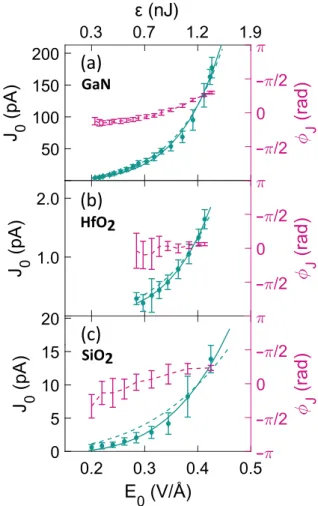
An important characteristic is the pulse intensity or equivalently the field amplitude (E0) dependence of the current signal because the order of nonlinearity of the dependence can provide insight about the excitation process taking place between the valence and conduction bands of the given material. Such an approach is coherent with previous studies that related the current control to the process of coherent superposition of wave packets originating from different excitation pathways [10,16]. Similar concepts are also widely applied in the multiphoton ionization of gases [22] as well as in solid-state media [16,23]. Therefore, we performed a laser power scan of the current signal from GaN, HfO2, and SiO2
media, as shown in Fig.4. The average power of the pulse train was measured right before the focusing parabola with a thermo- pile power meter head. The pulse energyεand the amplitude of the field amplitudeE0in the target medium was calculated from the measured focal spot size and the d-scan-reconstructed pulse duration. The finite reflectivity of the parabolic mirror and Fresnel reflection from the surface of the sample were taken into account.
Positioning of the target into the focus was performed by manual search for the maximum current signal while adjusting thex y z coordinates of the target with submicron-precision actuators.
Multiple power scans were performed for each material, out of which the average value ofJ0is displayed in Fig.4together with error bars representing the standard deviation across the set of mea- surements. Along with the magnitude of current, we also measured the phase of the signal. The phase was stable during the time of the measurement, which took only a few minutes. As it can be seen, the increase of signal with the field strength is different for the cases of GaN, HfO2, and SiO2. This could be related to the order of nonlinearity of the current generation process involved, which depends on the bandgap Eg and the photon energy. Assuming excitation ofreal carriers and the current originating from the interference of multiple multiphoton pathways, the expected relationship [10] between the signal and the E-field would hold:
J0∝E02N+1, whereN=Eg
~ωis the number of photons needed to populate the conduction band. Considering the range of photon
Fig. 4. Dependence of the total current amplitude,J0 (green), and its phase,φJ (magenta), on the electric field strength,E0, measured at the reference frequency fceo. It is shown for targets made from (a) GaN, (b) HfO2, and (c) SiO2. All targets were measured with a focal spot size of 1.8µm. Abscissa on the top serves to show nonlinear scaling with pulse energy. A vertical offset was applied to the phase to center the mean of the phase to zero. Dashed green curves were obtained by fitting according to the model described in Eq. (1). The solid line was obtained using the same model extended with a correction, taking into account the expansion of the surface that contributes to the current generation as the intensity is increased.
energies included in the ultrabroadband laser spectrum, as shown in Fig.1(b), one can consider multiphoton transitions between the valence and conduction band with a multiplicity of two to three photons in case of GaN and five to nine photons in the SiO2 case. Hence, the exponent of the curve would be between five and seven for GaN and at least 11 for SiO2. Power fitsJ0∝E0qapplied to the results (not shown) provideq=6.3 and 5.6 for these two materials, respectively. Although this would explain the slope in the GaN measurement, it cannot explain the data for SiO2, where the exponent differs by more than five. This means that perturba- tion theory considering multiphoton transitions and exciting real carriers cannot be effectively applied to the range of parameters and materials under investigation, especially not for SiO2; thus, a different model must be applied.
For a better description of the observed field-strength depend- encies for all investigated materials, we turned toward Khurgin’s model, as described in [24]. This model was applied successfully for current control results in GaN [9]. In this model, the current is a consequence of a photogalvanic effect in aχ(3)-type medium
via nonlinear conductivity. The three photon interference [ω1, ω2,−(ω1+ω2)] generates the DC current; as soon as the par- ticipating photons have energy lower than the half of the band gap, no real charge carriers in the conduction band are populated.
Conversely, the concept of virtual carriers is introduced because the interband transitions also are featured in the mathematical descrip- tion. We compared our experimentally measured photo-induced J0(E0)currents with the theoretical curves obtained by applying Khurgin’s model. Within this model, we assume a femtosecond linearly polarized Gaussian pulse with a carrier frequency below bandgap frequency. The electric field of the pulse is defined as E(t)=E0exp(−2 ln 2t2/τ2p)cos(ω0t+φce)). The laser pulse induces an asymmetric distribution of virtual carriers in the con- duction and valence bands in the dielectric or semiconductor.
After the passage of the ultrashort laser pulse, a net charge Qis accumulated in the medium and
Q(E0)=ε0Aeffχ(3)
mmax
X
m=1
χ(3) χ(1)
m−1
ha2m+1iE02m+1, (1)
which flows to the circuit through the electrodes and produces a current J0∼Q(E0)/τRC, with τRC being an unknown char- acteristic time of the circuit. Aeff is a parameter that takes into account the efficient surface area of the target. According to this formula, the dimensionless ha2m+1i =ω0
Rha(t)2m+1idt odd-power moments of the normalized vector potential [i.e., a(t)=(ω0/E0)Rt
−∞E(t0)dt0] were numerically evalu- ated for the laser pulse parametersτp=5.5 fs andω0=2πc/λ, with λ=800 nm. A numerical convergence test was per- formed to obtain mmax and, for the considered field strengths, it yielded convergent results already for mmax=5 for each target material. For the first-order susceptibility, we consid- ered χ(1)=n2−1, with n being the refractive index of the target material. Finally, a fitting was performed to find values for Aeff/τRC using table values for third-order susceptibil- ity χ(3) for GaN: χ(3)=2.1×10⁻²⁰m2/V2 [25] and SiO2: χ(3)=2×10⁻²²m2/V2[26]. An approximate value of the third- order susceptibility for HfO2was obtained from Miller’s relation [27] asχ(3)=3.5×10⁻²¹m2/V2.
Results of the fits using Khurgin’s model are presented with dashed lines in Fig. 4. We obtained satisfactory results for all targets. Yet, for SiO2 the model underestimates the steepness of the curve. To rectify this discrepancy, we amended the model to take into account the effects of the size of the illuminated area on the sample. The inherent property of Khurgin’s model is that it assumes constant E-field strength across the area in the focal plane. As we operate our experiment in a tight focusing regime (as opposed to previous similar studies [9,10]), the effect of the nonuniform illumination might become significant. Therefore, we added a correction factor to Eq. (1), taking into account that the area above some critical value of field strength Ecritincreases with applied E-field amplitude E0. The value Ecrit represents a threshold from where the effect starts to appear. This value also depends on the material. HavingEcritand the laser waistw0fixed, the E-field profile of the area illuminated by a Gaussian laser is given as E(r)=E0exp(−2r2/w02). Hence, the radiusrc of the area contributing to the current generation, defined asE >Ecrit, is obtained from Ecrit=E(rc). From there, it can be deduced that the effective area scales with the field amplitude according to Aeff(E0)∝πw20lnE0/Ecrit. Considering this, we amended the fits obtained from the model in Eq. (1), as shown by the solid
lines in Fig.4.Ecritvalues were taken as new parameters for the fit and their values were determined to be 0.06, 0.12, and 0.17 V/Å for GaN, HfO2, and SiO2, respectively. Notice that this sequence of critical fields corresponds to the increasing bandgap of the targets (3.5 eV, 5.9 eV, and 9.0 eV, respectively). We note that, in case of GaN, the phenomenon is observable even for lower field amplitudes than presented in Fig.4(a). Our analysis ofEcritindi- cates that the effect can be initiated already with 0.06 V/Å, which corresponds to∼50 pJ of pulse energy.
With measurement curves reproduced well with the model in Fig.4, it remains to elucidate the background of the different field dependencies observed. A different slope is particularly noticeable for the GaN and the SiO2samples depicted in Figs.4(a) and4(c), respectively. Going deeper in the details of the model from Eq. (1), we can show that the slope is determined by the material constant χ(3)and its relation to the appliedE0amplitude and the value of coefficientsha2m+1i. This is becauseχ(3) can be approximately related to the atomic fieldEa asχ(3)∼Ea−2[24]. When applied to Eq. (1), one can see that the significance of individual terms in the expansion is given by the ratioE0/Ea. The closer the ratio is to one, the higher the contribution of higher-order terms. Moreover, the coefficientsha2m+1ican have orders of magnitude different val- ues. For example, for the considered pulse of 5.5 fs duration,a7is 150 times higher thena3. Analysis of the contributions of the indi- vidual terms shows that the GaN curve in Fig.4(a) is determined mostly by terms of fifth- and seventh-order. SiO2 is determined by the 3rd order with little contribution from the fifth order and finally HfO2 is defined by more or less equal contributions of the third- and fifth-order terms. For more details, see Fig. S3 in Supplement 1, where the individual terms from the expansion in Eq. (1) are plotted.
Another interesting feature is the phase dependence of the sig- nal. The measurement shows that the phase of the current has very low field amplitude dependence for all materials, as shown by the purple line in Fig.4. From 0.2 V/Å to the maximum probed inten- sity about 0.4 V/Å the phase is slightly monotonically increasing with field strength. This could be a promising property for a CEP detector for online phase tagging applications [17,28] used with laser oscillators. For example, a robust phase characterization could be performed with a pulse providing an electric field strength on the GaN target between 0.2 and 0.3 V/Å where the phase change in this interval is almost flat and changes only by 12◦.
Note that there are contrasting models for transient metal- lization presented in the literature [6,13,23,24] and obtaining a phase-sensitive current for such low field strengths in case of the SiO2target is a striking finding. In the originally introduced picture [6,13], the strong, but adiabatic, optical fields shift the original valence and conduction bands to create a new state of matter formed by so-called Wannier–Stark ladders. This model requires high electric fields of∼1 V/Å to allow transitions between the Wannier–Stark shifted valence and conduction band of directly neighboring lattice sites. The observation of the phenomenon with a lower field suggests that transitions between remote sites of the lattice are not negligible. A more recent model by Chenet al. [23]
builds upon the interaction between the valence and conduction bands of the dielectric at the terminal crystal cells with the Fermi sea of electrons in the electrodes. Transient states are created where the electrons from the metal have enough energy (in relation to the conduction band) and they can hop to the conduction band, resulting in a current. A condition arises from this reasoning that
the process can be triggered only for fields higher than 1.4 V/Å.
Unlike other models, this one even predicts opposite CEP for which the maximum current is achieved. In spite of that, our obser- vation shows that it is possible to achieve current control well below this limit and the role of electrodes in the process still must be dis- cussed. Apparently, understanding of the transient metallization in wide-bandgap materials is yet to be settled and new observations and measurements for a different set of parameters and materials are needed.
4. SUMMARY
In summary, we demonstrated light-field-driven control of optically induced currents in dielectrics and wide-bandgap semi- conductors with unprecedentedly low, pJ-level laser pulse energy and 80 MHz repetition rate. Despite the fact that the currents were detected with slow circuitry, the directional sensitivity of the measured current to the subcycle evolution of the CEP underpins the sub-PHz bandwidth nature of the interaction between the laser and the dielectric (semiconductor) medium and electrode.
Applying a theoretical model to our data, we could explain the dependence of the signal on the electric field amplitude of the laser pulse, which supports the understanding of these currents as a nonresonant phenomenon. In other words, even when real carriers cannot be produced by multiphoton transitions, virtual carriers are being generated and their distribution in momentum space, being asymmetric due to the nonzero time-integral of the laser vector potential, produces real currents detected by external circuitry. Consequently, our data indicate that current control can be obtained for pulses as weak as 50 pJ. The fact that the phase of the detected current is insensitive to the pulse energy hints at the possibility to design robust CEP detectors of laser oscillator pulses. With the results demonstrated, we believe our experiments pave the way toward ultrafast, PHz-bandwidth optoelectronic devices operational with pJ-level pulse energy being instru- mental for future, real-life applications of ultrafast, integrated optoelectronics.
Funding. Nemzeti Kutatási Fejlesztési és Innovációs Hivatal (2018- 1.2.1-NKP-2018-00012, VEKOP-2.3.2-16-2017-00015); Horizon 2020 Framework Programme (FETOPEN-PetaCOM, MULTIPLY); Deutsche Forschungsgemeinschaft (SFB 1375 - 398816777); Fraunhofer-Gesellschaft (066-601020).
Acknowledgment. Author Péter Dombi acknowledges support from the Eötvös Research Network and the Hungarian Academy of Sciences. Author Zilong Wang acknowledges support from the EU via the MULTIPLY program, and from the AvH via a research fellowship. Author Matthias F. Kling is grateful for support from the Max Planck Society.
Disclosures. The authors declare no conflicts of interest.
Data Availability. Data underlying the results presented in this paper are not publicly available at this time but may be obtained from the authors upon reason- able request.
Supplemental document. SeeSupplement 1for supporting content.
REFERENCES
1. ß, P. Dombi, Z. Pápa, J. Vogelsang, S. V. Yalunin, M. Sivis, G. Herink, S.
Schäfer, P. Gro, C. Ropers, and C. Lienau, “Strong-field nano-optics,”
Rev. Mod. Phys.92, 025003 (2020).
2. F. Krausz and M. I. Stockman, “Attosecond metrology: from electron capture to future signal processing,”Nat. Photonics8, 205–213 (2014).
3. T. Rybka, M. Ludwig, M. F. Schmalz, V. Knittel, D. Brida, and A.
Leitenstorfer, “Sub-cycle optical phase control of nanotunnelling in the single-electron regime,”Nat. Photonics10, 667–670 (2016).
4. Y. Yang, M. Turchetti, P. Vasireddy, W. P. Putnam, O. Karnbach, A. Nardi, F. X. Kärtner, K. K. Berggren, and P. D. Keathley, “Light phase detection with on-chip petahertz electronic networks,”Nat. Commun.11, 3407 (2020).
5. T. Higuchi, L. Maisenbacher, A. Liehl, P. Dombi, and P. Hommelhoff, “A nanoscale vacuum-tube diode triggered by few-cycle laser pulses,”
Appl. Phys. Lett.106, 051109 (2015).
6. A. Schiffrin, T. Paasch-Colberg, N. Karpowicz, V. Apalkov, D. Gerster, S. Mühlbrandt, M. Korbman, J. Reichert, M. Schultze, S. Holzner, J. V.
Barth, R. Kienberger, R. Ernstorfer, V. S. Yakovlev, M. I. Stockman, and F.
Krausz, “Optical-field-induced current in dielectrics,”Nature493, 70–74 (2013).
7. O. Kwon, T. Paasch-Colberg, V. Apalkov, B. K. Kim, J. J. Kim, M. I.
Stockman, and D. Kim, “Semimetallization of dielectrics in strong optical fields,”Sci. Rep.6, 1–9 (2016).
8. M. Durach, A. Rusina, M. F. Kling, and M. I. Stockman, “Predicted ultra- fast dynamic metallization of dielectric nanofilms by strong single-cycle optical fields,”Phys. Rev. Lett.107, 2–6 (2011).
9. F. Langer, Y.-P. Liu, Z. Ren, V. Flodgren, C. Guo, J. Vogelsang, S.
Mikaelsson, I. Sytcevich, J. Ahrens, A. L’Huillier, C. L. Arnold, and A.
Mikkelsen, “Few-cycle lightwave-driven currents in a semiconductor at high repetition rate,”Optica7, 276–279 (2020).
10. T. Paasch-Colberg, S. Y. Kruchinin, Ö. Sa ˘glam, S. Kapser, S. Cabrini, S. Muehlbrandt, J. Reichert, J. V. Barth, R. Ernstorfer, R. Kienberger, V. S. Yakovlev, N. Karpowicz, and A. Schiffrin, “Sub-cycle optical control of current in a semiconductor: from the multiphoton to the tunneling regime,”Optica3, 1358–1361 (2016).
11. T. Higuchi, C. Heide, K. Ullmann, H. B. Weber, and P. Hommelhoff,
“Light-field-driven currents in graphene,”Nature550, 224–228 (2017).
12. P. Földi, I. Márton, N. Német, V. Ayadi, and P. Dombi, “Few-cycle plas- mon oscillations controlling photoemission from metal nanoparticles,”
Appl. Phys. Lett.106, 013111 (2015).
13. M. Schultze, E. M. Bothschafter, A. Sommer, S. Holzner, W.
Schweinberger, M. Fiess, M. Hofstetter, R. Kienberger, V. Apalkov, V. S. Yakovlev, M. I. Stockman, and F. Krausz, “Controlling dielectrics with the electric field of light,”Nature493, 75 (2013).
14. A. Haché, Y. Kostoulas, R. Atanasov, J. L. P. Hughes, J. E. Sipe, and M. Glasbeek, “Observation of coherently controlled photocurrent in unbiased, bulk GaAs,”Phys. Rev. Lett.78, 306–309 (1997).
15. T. M. Fortier, P. A. Roos, D. J. Jones, S. T. Cundiff, R. D. R. Bhat, and J. E. Sipe, “Carrier-envelope phase-controlled quantum interference of injected photocurrents in semiconductors,”Phys. Rev. Lett.92, 1–4 (2004).
16. P. A. Roos, X. Li, J. A. Pipis, T. M. Fortier, S. T. Cundiff, R. D. R. Bhat, and J. E. Sipe, “Characterization of carrier-envelope phase-sensitive pho- tocurrent injection in a semiconductor,”J. Opt. Soc. Am. B22, 362–368 (2005).
17. T. Paasch-Colberg, A. Schiffrin, N. Karpowicz, S. Kruchinin, Ö. Sa ˘glam, S. Keiber, O. Razskazovskaya, S. Mühlbrandt, A. Alnaser, M. Kübel, V.
Apalkov, D. Gerster, J. Reichert, T. Wittmann, J. V. Barth, M. I. Stockman, R. Ernstorfer, V. S. Yakovlev, R. Kienberger, and F. Krausz, “Solid-state light-phase detector,”Nat. Photonics8, 214–218 (2014).
18. S. Sederberg, D. Zimin, S. Keiber, F. Siegrist, M. S. Wismer, V. S.
Yakovlev, I. Floss, C. Lemell, J. Burgdörfer, M. Schultze, F. Krausz, and N. Karpowicz, “Attosecond optoelectronic field measurement in solids,”Nat. Commun.11, 430 (2020).
19. S. Rausch, T. Binhammer, A. Harth, J. Kim, R. Ell, F. X. Kärtner, and U.
Morgner, “Controlled waveforms on the single-cycle scale from a fem- tosecond oscillator,”Opt. Express16, 9739–9745 (2008).
20. M. Miranda, M. Kotur, P. Rudawski, C. Guo, A. Harth, A. L’Huillier, and C. L. Arnold, “Spatiotemporal characterization of ultrashort laser pulses using spatially resolved Fourier transform spectrometry,”Opt. Lett.39, 5142–5145 (2014).
21. P. Dombi, A. Apolonski, C. Lemell, G. G. Paulus, M. Kakehata, R.
Holzwarth, T. Udem, K. Torizuka, J. Burgdörfer, T. W. Hänsch, and F.
Krausz, “Direct measurement and analysis of the carrier-envelope phase in light pulses approaching the single-cycle regime,”New J. Phys.6, 39 (2004).
22. S. L. Chin, C. Rolland, P. B. Corkum, and P. Kelly, “Multiphoton ioniza- tion of Xe and Kr with intense 0.62-µm femtosecond pulses,”Phys. Rev.
Lett.61, 153–156 (1988).
23. L. Chen, Y. Zhang, G. Chen, and I. Franco, “Stark control of electrons along nanojunctions,”Nat. Commun.9, 1–12 (2018).
24. J. B. Khurgin, “Optically induced currents in dielectrics and semicon- ductors as a nonlinear optical effect,”J. Opt. Soc. Am. B33, C1–C9 (2016).
25. J. Miragliotta and D. K. Wickenden, “Optical third-harmonic studies of the dispersion in X–(3)for gallium nitride thin films on sapphire,”Phys.
Rev. B50, 14960–14964 (1994).
26. D. Milam, “Review and assessment of measured values of the nonlin- ear refractive-index coefficient of fused silica,”Appl. Opt.37, 546–550 (1998).
27. W. Ettoumi, Y. Petit, J. Kasparian, and J.-P. Wolf, “Generalized Miller formulæ,”Opt. Express18, 6613–6620 (2010).
28. A. M. Sayler, T. Rathje, W. Müller, K. Rühle, R. Kienberger, and G. G.
Paulus, “Precise, real-time, every-single-shot, carrier-envelope phase measurement of ultrashort laser pulses,”Opt. Lett.36, 1–3 (2011).