Proceedings 2020, 4, x; doi: FOR PEER REVIEW www.mdpi.com/journal/proceedings Proceedings
Ab-initio wave packet dynamical simulation of defects in 2D materials
†Géza I. Márk 1, *, and Péter Vancsó 1
1 Research Institute for Technical Physics and Materials Science, H-1525 Budapest, P.O.Box 49, Hungary
* Correspondence: mark@mfa.kfki.hu
† Presented at 1st International Electronic Conference on Applied Sciences, 10–30 November 2020; Available online: https://asec2020.sciforum.net/.
Published: 10 November 2020
Abstract: Materials consisting of a single layer of atoms have many promising applications, due to their extraordinary physical properties. These properties, however, depend on the density and kind of structural defects present in the perfect 2D crystalline lattice. Electrons with energies falling into the allowed band propagate freely in a perfect crystal, but defects act as scattering centers for the Bloch waves. We studied the influence of structural defects on the transport properties of a graphene lattice by calculating the scattering of electronic wave packets. We compared two methods. i) Description of the atomic lattice and the electronic structure of graphene by an atomic pseudopotential, then calculation of the Bloch functions and corresponding E(kBloch) energies. The defect is represented by a local potential, then we compute the scattering by the time development of a wave packet composed of the Bloch waves. ii) If we he incorporate the E(kBloch) dispersion relation directly into the kinetic energy operator, however, we don’t need to calculate the wave functions, thus we also don’t need the graphene potential. The dispersion relation can be a simple tight-binding (TB) dispersion relation, but for a more accurate representation of the electronic structure, we can utilize E(kBloch) dispersion relations from an ab-initio DFT calculation.
Keywords: wave packet dynamics; graphene; transport properties; band structure; vacancy
1. Introduction
In order to design nanoelectronic devices, it is important to precisely understand the dynamics of electrons in these structures. Wave packet dynamics (WPD) [1] can simulate electronic dynamics and transport phenomena at the nanoscale and is capable of calculating realistic models containing several hundred atoms already on a personal computer. The physical system is described by a Hamiltonian and the initial conditions are given by an initial wave function. Solution of the time dependent Schrödinger equation then yields the 𝜓(𝑟⃗, 𝑡) time dependent wave function and its time- energy Fourier transform gives the 𝜓(𝑟⃗, 𝐸)energy dependent wave function. In the one particle approximation we calculate only a one (quasi)particle three-dimensional (3D) wave function instead of the 3N dimensional many body wave function and the details of the many body interaction are coded into the Hamilton operator. This can be done by building a sufficient 𝑉(𝑟⃗)one particle pseudopotential. During the past two decades we have been performing WPD calculations [2]–[4] for many sp2 Carbon nanosystems, by using a variationally calculated local Carbon one electron pseudopotential [5]. This potential has two major advantages: i) it brings the specific electronic dynamics (linear dispersion near the K points for electrons near the Fermi energy (EF), trigonal warping for hot electrons, etc) of the bands [6] into the WPD calculation and ii) makes it possible to handle localized defects. We were able to exploit this feature of the pseudopotential in calculating the transport properties of different 0D and 1D graphene defects [3,7].
The WPD calculation has two input quantities: i) the Hamiltonian and ii) the 𝜓0(𝑟⃗) = 𝜓(𝑟⃗, 𝑡 = 0) initial state. In our former calculations 𝜓0(𝑟⃗) was a simple 3D Gaussian wave packet (WP), but this made it necessary to start the initial WP from a region of space, where 𝑉(𝑟⃗) = 0, or at least constant, and the WP had to be injected from this region into the nanosystem through a simulated interface layer. This, however, made it difficult to create a WP with pre-determined initial spectrum on the nanosystem, because the interface layer can considerably distort the spectrum.
We can, however, build a tailor-made initial WP on the nanosystem if we construct the WP as a superposition of Bloch states. This is what we present in Sec. 2 of this work and then these precisely determined WPs were used to study scattering in defect states.
In Sec. 3 we introduce and apply an alternative WPD technique, which has the advantage that it completely circumvents the need to calculate a pseudopotential. We work out the time evolution of the WP directly from the 𝐸(𝑘⃗⃗𝐵𝑙𝑜𝑐ℎ) dispersion relation. Formerly we applied [2] this method for studying the WPD on a graphene and a MoS2 single layer and now we test it for graphene structural defects.
2. Bloch function wave packet construction, time evolution, and scattering in graphene
For any 𝑉(𝑟⃗) potential which is periodic in space, the solutions of the stationary Schrödinger equation have the form of 𝜑(𝑟⃗, 𝑘⃗⃗𝐵𝑙𝑜𝑐ℎ) = 𝑢(𝑟⃗, 𝑘⃗⃗𝐵𝑙𝑜𝑐ℎ)𝑒𝑖𝑘⃗⃗𝐵𝑙𝑜𝑐ℎ𝑟⃗, where 𝑢(𝑟⃗, 𝑘⃗⃗𝐵𝑙𝑜𝑐ℎ) is a periodic function and 𝑘⃗⃗𝐵𝑙𝑜𝑐ℎ is the Bloch wave vector. These 𝜑(𝑟⃗, 𝑘⃗⃗𝐵𝑙𝑜𝑐ℎ) functions are called Bloch functions.
Bloch functions and the corresponding 𝐸(𝑘⃗⃗𝐵𝑙𝑜𝑐ℎ) energies can be easily computed numerically for any periodic potential, with the Fourier transformed form of the Schrödinger equation. Figure 1.
shows some characteristic Bloch functions for the graphene surface, computed using the graphene pseudopotential [5].
Next, we constructed localized wave packets as a superposition of Bloch states. It is possible to build maximally localized Wannier functions [9], [10], [11] by a carefully chosen superposition, but those superpositions span for the whole Brillouin zone. If we want to have a fairly narrow spectral distribution together with a sufficiently narrow spatial distribution, we can use a superposition with a simple Gaussian amplitude function 𝑎(𝑘⃗⃗):
𝜙(𝑟⃗) = ∫ 𝑒−
|𝑘⃗⃗−𝑘⃗⃗0|2
4∆𝑘2 𝑒𝑖𝑟⃗0𝑘⃗⃗ 𝜑(𝑟⃗, 𝑘⃗⃗)𝑑3𝑘⃗⃗ (1)
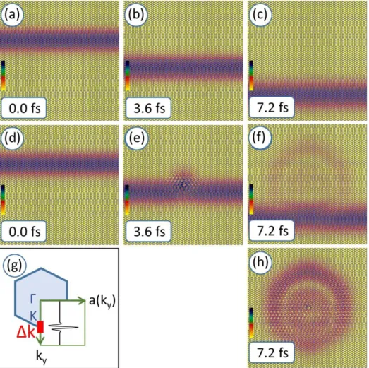
where we wrote 𝑘⃗⃗ for 𝑘⃗⃗𝐵𝑙𝑜𝑐ℎ in this formula for brevity (see Appendix A), 𝑘⃗⃗0 is the momentum space, 𝑟⃗0 is the direct space initial position of the Gaussian and ∆𝑘 is its momentum width. Figure 2a shows a such constructed WP, localized in its 𝑦 coordinate in direct space and its spectrum is concentrated on one of the graphene 𝐾 points, Fig 2g is the plot of the real part of the 𝑎(𝑘⃗⃗) amplitude function. It is a Gaussian multiplied with a plane wave.
Figures 2a-c show the time evolution of this Bloch WP for an unperturbed graphene lattice. This was calculated by numerically solving the time dependent Schrödinger equation with the split- operator FFT method [12], [13], [14] using the 𝐻̂ = 𝐾̂𝑓𝑟𝑒𝑒+ 𝑉̂ Hamilton operator, where 𝐾̂𝑓𝑟𝑒𝑒 is the free space kinetic energy operator and 𝑉̂ = 𝑉(𝑟⃗) is the graphene pseudopotential [5]. This time evolution – i.e. that for the infinite lattice – can also be analytically calculated by inserting the 𝐸𝑥𝑝[−𝑖𝐸(𝑘⃗⃗𝐵𝑙𝑜𝑐ℎ)𝑡] time propagator into the kernel of Eq.1, where 𝐸(𝑘⃗⃗𝐵𝑙𝑜𝑐ℎ) is the graphene dispersion relation. The WP moves in the −𝑦 direction, because its spectral distribution is centered at the lowest K point of the graphene Brillouin zone. The spectral width of the WP is small, 0.1𝛤𝐾̅̅̅̅, hence the dispersion relation is still linear, there is only a very small spreading in the time evolution, the shape of the WP remains unchanged.
Figures d-f show the time evolution of the same initial Bloch WP on a graphene lattice with a structural defect. We can see that the WP is indeed scattered on the defect and the angular distribution of the scattered WP has a hexagonal symmetry.
Figure 1. Construction of the graphene Bloch wave functions for different points along the ΓK line in the extended Brillouin zone. Left column: 𝑒𝑖𝑘⃗⃗𝐵𝑙𝑜𝑐ℎ𝑟⃗. Middle column: 𝑢(𝑟⃗, 𝑘⃗⃗𝐵𝑙𝑜𝑐ℎ). Right column:
𝜑(𝑟⃗, 𝑘⃗⃗𝐵𝑙𝑜𝑐ℎ). See Sec.1. for details. Real parts of the wave functions are shown, green is positive, red is negative. The graphene lattice is shown by blue lines. The insets in a, d, g, j show the position of 𝑘⃗⃗𝐵𝑙𝑜𝑐ℎ (yellow dot) relative to the Brillouin zone.
3. Band structure governed wave packet dynamics
In the traditional formulation of the WPD the environment of the moving electron quasiparticle (i.e. the crystal and the averaged effect of the other electrons) is incorporated into the potential energy operator by the help of a (pseudo)potential, thus the Hamiltonian is 𝐻̂ = 𝐾̂𝑓𝑟𝑒𝑒+ 𝑉̂. In this Section we present an alternative formulation, where the effect of the crystal potential and the many-body effects are incorporated into the kinetic energy operator, i.e. the Hamiltonian is 𝐻̂ = 𝐾̂ + 𝑉̂𝑓𝑟𝑒𝑒.
Figure 2. Time evolution of the probability density of a Bloch function wave packet in the graphene pseudopotential. (a,b,c) Without defect. (d,e,f) With defect. (g) Spectral distribution of the Bloch function wave packet in the Brillouin zone, only the real part of 𝑎(𝑘⃗⃗) is shown. The red bar shows the reciprocal space width Δ𝑘. (h) Scattering pattern, absolute value of the difference of the WPs shown on (c) and (f). The size of the calculation window is 14.48 nm.
Thus 𝐻̂ = 𝐾⃗⃗⃗𝑓𝑟𝑒𝑒, because the potential energy of a free particle is zero, 𝑉̂𝑓𝑟𝑒𝑒= 0. All of crystal structure and electronic structure effects are taken care of in band structure calculations which yield a dispersion relation 𝐸𝑛(𝑘⃗⃗𝐵𝑙𝑜𝑐ℎ), where is the Bloch wave vector and n is the band index. The kinetic energy operator in free space is 𝐾̂𝑓𝑟𝑒𝑒 =|𝑘⃗⃗|
2
2 = 𝐸𝑓𝑟𝑒𝑒(𝑘⃗⃗) in momentum representation, where 𝐸𝑓𝑟𝑒𝑒(𝑘⃗⃗) is the free space dispersion relation. In our alternative formulation we replace the free space dispersion relation with the one describing the dispersion relation of a many electron system in a given crystalline material, thus the momentum representation of the kinetic energy operator is 𝐾̂ = 𝐸(𝑘⃗⃗𝐵𝑙𝑜𝑐ℎ). We already presented such calculations for perfect 2D crystals, graphene and MoS2 single sheets in [2]. Those calculations successfully reproduced the trigonal warping effect and the anisotropic WP spreading characteristic of these 2D materials and showed different symmetries of the WP spreading, depending on the band structure and the spectral distribution of the initial WP.
As we emphasized in [2], similar calculations can be easily performed for any crystalline material, where the dispersion relation is known.
In this Section, we combine the two methods, in order to study defects in 2D crystalline materials. We describe the (infinite, periodic) crystal by the kinetic energy operator (utilizing the dispersion relation of that material) and the structural defect by a local potential. Thus our Hamiltonian will become 𝐻̂ = 𝐾̂𝑐𝑟𝑦𝑠𝑡𝑎𝑙+ 𝑉̂𝑑𝑒𝑓𝑒𝑐𝑡, where the 𝐾̂𝑐𝑟𝑦𝑠𝑡𝑎𝑙 = 𝐸(𝑘⃗⃗𝐵𝑙𝑜𝑐ℎ) kinetic energy operator describes the electronic structure of the crystal lattice and the 𝑉̂𝑑𝑒𝑓𝑒𝑐𝑡= 𝑉(𝑟⃗) potential energy operator describes the local defect.
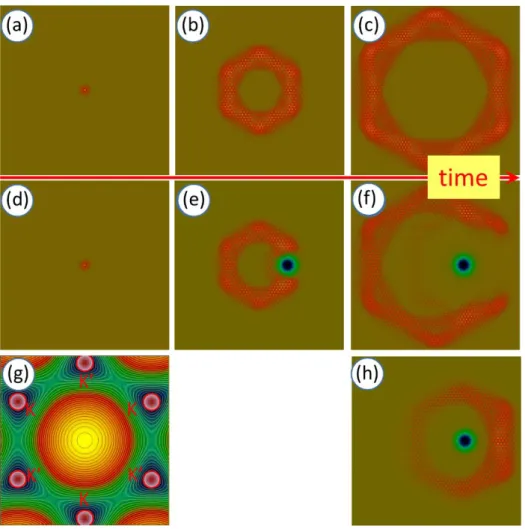
Figures 3a-c show the time evolution of a WP for an unperturbed graphene lattice and Figs 3d-f is the same time evolution with a local defect. The WPD was calculated by numerically solving the time dependent Schrödinger equation with the split-operator FFT method [12], [13], [14]. T spectral distribution of the initial WP is a sum of six Gaussians, placed in the six K and K’ points (Fig 3g).
Figure 3. Time evolution of the probability density of a wave packet on the graphene surface with- and without defect. The band structure of the perfect crystal is incorporated into the kinetic energy operator, hence the potential is everywhere zero, except in the defect region. (a,b,c) Without defect.
(d,e,f) With defect. The defect is shown by a blue spot. (g) Spectral distribution of the initial wave packet in the Brillouin zone (absolute value) is shown by red circles in the K and K’ points, superimposed on the graphene band structure. The radius of the red circles is Δ𝑘/2, the intensity of the red color is proportional to the spectral weight at each (𝑘⃗⃗𝑥, 𝑘⃗⃗𝑦) points. (h) Scattering pattern, absolute value of the difference of the WPs shown on (c) and (f). The size of the calculation window is 23.04 nm.
Several important effects can be seen in these images. Firstly, in the case of the unperturbed graphene surface, we can see an anisotropic (hexagonal) spreading of the WP. This is in agreement with our earlier calculations [4], where the initial WP was injected onto the graphene surface from an STM tip and also with TB-DFT calculations in [15]. Secondly, an atomic scale modulation is present on the WP. This is interesting, because this calculation does not directly have the atomic lattice as input. The atomic structure is, however, implicitly represented by the graphene dispersion relation.
Thirdly, when the WP hits the local potential, it is scattered on it. Though the local potential is cylindrically symmetric (isotropic), the scattered WP has a hexagonal symmetry (anisotropic) – as is best seen on the difference image in Fig 3h. This effect, which can be termed as a “generalized Huygens principle” is caused by the anisotropic nature of the graphene dispersion relation.
4. Conclusions
We presented an extension to the wave packet dynamical method, where the initial wave packet is constructed from the numerically calculated Bloch states of the pseudopotential representing the physical system. This method makes it possible to fine-tune the spectral distribution of the initial wave packet and thus investigate the details of the nanoscale transport phenomena for different scenarios. The method was then applied for a structural defect on a graphene surface where we studied the scattering of the Bloch function wave packet on the local defect. A hexagonal scattering pattern was seen.
Then we went on to calculate the wave packet time evolution by a method, where the properties of the infinite crystal (its atomic- and electronic structure) is coded into the kinetic energy operator and the properties of the local defect is represented by a local potential. An anisotropic (hexagonal) scattering pattern emerges even for an isotropic (Gaussian) potential, because of the anisotropic nature of the band structure. The advantage of the method is that it does not require the calculation of a pseudopotential. The only input necessary to represent the infinite crystal is its 𝐸(𝑘⃗⃗𝐵𝑙𝑜𝑐ℎ) band structure, available from, for example, a DFT calculation.
Supplementary Materials: The following are available online at http://www.xxxxx, Video S1: Time development of a wave packet on the graphene surface. Video S2: Scattering of a wave packet on a graphene defect.
Author Contributions: Conceptualization, methodology, software, G.I.M; writing—original draft preparation, G.I.M.; writing—review and editing, V.P.
Funding: The work was supported by the European H2020 GrapheneCore2 project no. 785219, Graphene Flagship a˛nd by the Hungarian National Research, Development and Innovation Office (grant no. KH130413).
Conflicts of Interest: The authors declare no conflict of interest.
Appendix A
In this paper the kinetic energy operator is defined in momentum space and the potential energy operator is defined in direct space. This is well suited to the calculation method, because we solve the time dependent Schrödinger equation by the split-time FFT method, where in each time step ∆𝑡 we change the wave function from the direct- to the reciprocal space and back by Fourier transforms. We have to emphasize that the term “Fourier transform” is used in two distinct meanings in this context.
The split-time FFT method uses the Fast Fourier Transform (FFT), which decomposes the wave function into plane waves, represented by 𝑘⃗⃗ wave vectors. In a crystalline material, described by a periodic potential, 𝑘⃗⃗ is not a good quantum number, but the crystal momentum 𝑘⃗⃗𝐵𝑙𝑜𝑐ℎ is. The momentum wave function 𝜑(𝑘⃗⃗𝐵𝑙𝑜𝑐ℎ) can be computed from the direct space wave function 𝜑(𝑟⃗) by applying a generalized Fourier transform, where the basis functions are the Bloch waves corresponding to the 𝑉(𝑟⃗) potential.
References
1. Garraway, B.M.; Suominen, K.-A. Wave-packet dynamics: new physics and chemistry in femto-time. Rep.
Prog. Phys. 1995, 58, 365–419.
2. Márk, G. I.; Fejér, G.R.; Vancsó, P.; Lambin, P.; Biró, L.P. Electronic Dynamics in Graphene and MoS2 Systems. Phys. Status Solidi Basic Res. 2017, 254 (11), 1700179.
3. Vancsó, P.; Márk, G. I.; Lambin, P.; Mayer, A.; Hwang, C.; Biró, L.P. Effect of the disorder in graphene grain boundaries: A wave packet dynamics study. Appl. Surf. Sci. 2014, 291, 58–63.
4. Márk, G.I.; Vancsó, P.; Hwang, C.; Lambin, P.; Biró, L.P. Anisotropic dynamics of charge carriers in graphene. Phys. Rev. B - Condens. Matter Mater. Phys. 2012, 85(12), 125443.
5. Mayer, A. Band structure and transport properties of carbon nanotubes using a local pseudopotential and a transfer-matrix technique. Carbon 2004, 42, 2057–2066.
6. Márk, G.I.; Biró, L.P.; Lambin, P. Calculation of axial charge spreading in carbon nanotubes and nanotube {Y}-junctions during {STM} measurement. Phys. Rev. B 2004, 70, 115411–115423.
7. Vancsó, P.; Márk, G.I.; Lambin, P.; Mayer, M.; Kim,Y.-S.; Hwang, C.; Biró, L.P. Electronic transport through ordered and disordered graphene grain boundaries. Carbon 2013, 64, 101–110.
8. Márk, G.I.; Biró, L.P.; Lambin, P. Calculation of axial charge spreading in carbon nanotubes and nanotube Y junctions during STM measurement. Phys. Rev. B - Condens. Matter Mater. Phys. 2004, 70(11), 115423.
9. Kohn, W. Analytic properties of Bloch waves and Wannier functions. Phys. Rev. 1959, 115 (4), 809–821.
10. Marzari, N.; Mostofi, A.A.; Yates, J.R.; Souza, I.; Vanderbilt, D. Maximally localized Wannier functions:
Theory and applications. Rev. Mod. Phys. 2012, 84(4), 1419–1475.
11. Bruzzone, S.; Iannaccone, G.; Marzari, N.; Fiori, G. An open-source multiscale framework for the simulation of nanoscale devices. IEEE Trans. Electron Devices. 2014, 61 (1), 48–53.
12. Fleck, J.A.; Morris, J.R.; Feit, M.D. Time-dependent propagation of high energy laser beams through the atmosphere. Appl. Phys. 1976, 10, 129–160.
13. Feit, M.D.; Fleck, J.A.; Steiger, A. Solution of the {S}chr{ö}dinger equation by a spectral method. J. Comput.
Phys. 1982, 47, 412–433.
14. Márk, G.I. Web-Schrödinger: Program for the interactive solution of the time dependent and stationary two dimensional (2D) Schrödinger equation. Available online: https://arxiv.org/abs/2004.10046 (accessed 4November on 2020).
15. Calogero, G.; Papior, N.; Koleini, M.; Larsen, M.H.L.; and M. Brandbyge. Multi-scale approach to first- principles electron transport beyond 100 nm. Nanoscale. 2019, 11(13), 6153–6164.
Publisher’s Note: MDPI stays neutral with regard to jurisdictional claims in published maps and institutional affiliations.
© 2020 by the authors. Submitted for possible open access publication under the terms and conditions of the Creative Commons Attribution (CC BY) license (http://creativecommons.org/licenses/by/4.0/).