Brain activity measurement with implantable microchip
Zoltán Kárász
A thesis submitted for the Doctor of Philosophy
Pazmany Peter Catholic University Faculty of Information Technology and Bionics Roska Tamas Doctoral School of Sciences and Technology
Supervisor Peter Foldesy, Ph.D.
Budapest, 2016
- 1 -
Introduction
The biomedical field is one of the most dynamically developing research area in the analog IC design, especially those concerning low-power implementation including implantable without battery. The examination procedures need more time for the functional result than available using other observing techniques as the FMRI or using simple EEG. Even though the portability of the measuring instrument is not an important issue for the animal studies, it is in the human experiments.
In the following, it will be presented in-vivo techniques currently used for brain activity recording in electrical engineering point of view. We have to understand what type of environment where the chip will be integrated. In our case where the main object to record electrical signals in the central nervous system. It is necessary to know what types of signal are we going to measure. Like what are the expected signal levels, frequencies or allowed noise levels. How the signal will be distorted by the tissue or the electrode itself and how it will be aging. The current solutions in literature do not deal with the low frequency distortion, based on the idea that information can be ignored. I will show the most widely accepted solutions then introduce a
- 2 -
new architecture which helps to optimize the noise and distortion levels at low frequencies.
Electrophysiological recording
The neuron is the basic unit for processing information in the human brain.
neurons transmit information by generating electronic pulses called spikes or action potentials. The neural signal most widely recorded is the extracellular bio-potential generated electrochemically by individual neurons. When a neuron receives sufficient stimuli from other cells, its cell membrane depolarizes, causing ionic currents to flow in its extracellular space. Consequently, an extracellular signal is generated from the electrical charge imbalance (among Na, K, Cl and other ions) near the outside of the biological membrane. The voltage drop associated with this extracellular single-unit action potential is a spike of about 50-500 μV in amplitude, with frequency content from 100 Hz to about 10 kHz. Normally, action potential waveforms (Fig. 1) are either bi-phasic or tri-phasic, were pulse widths are typically 1-1.5 ms. The noise floor, which includes biological noise from far field neurons and thermal noise from electrodes could be as high as 20 μVrms. Due to the unavoidable electrochemical effects at the electrode-tissue
- 3 -
interface, DC offsets ranging from 0.1-0.5 V across the recording sites.
Besides neuronal spikes, researchers are also interested in activities of large groups of neurons. The synchronous firing of many neurons near the electrode results in a low frequency oscillation, which is called the Local Field Potential (LFP).
Fig. 1 - Typical recorded neural signal
It can be classified by the types of recording:
- Intracellular (Patch-clamp electrode) - Extracellular
- Surface - Eidural - Scalp (EEG)
Because the extracellular solution gives the best spatial resolution and signal to noise ratio (except the patch-clamp which cannot be used in-vivo)
- 4 -
that is the generally accepted standard method in clinical circumstance.
Amplifier design
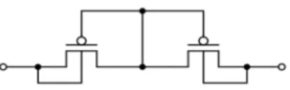
In order to record low frequency neural signals, the realization of large time constants is fundamental in the design. The filters are required to be tunable. In addition, realizations with low power dissipation and small size are also critical. The trivial solution to employ on-chip physical resistor and capacitor requires large chip area and it would not be tunable. The possible solutions can be categorized into pseudo-resistor implementations, switched-capacitor (SC) methods and operational trans-conductance amplifier capacitor (OTA-C) techniques with very small trans- conductance’s to allow the on-chip capacitance to be kept manageable low.
Fig. 2 - High-level schematic of the feedback neural amplifier
- 5 -
Using the linear-region MOS transistors to set the DC operating points of the feed-forward distributed-gain amplifier poses a severe problem since the thermal noise in the linear-region MOS transistors appears at the frontend, which is the most critical stage of any low-noise amplifier. Instead of achieving a low-noise performance, the feed-forward distributed-gain amplifier have a much higher total integrated input-referred noise than it was originally desired due to these biasing elements.
Fig. 3 - Amplifier schematic used in this design
The folded-cascode OTA (Fig. 3) offers many advantages over other OTA topologies for low-frequency applications if it is used in a feedback topology with a high closed-loop gain. The first advantage is that the frequency compensation of the feedback amplifier can be achieved with
- 6 -
simple dominant-pole compensation at the output since the internal nodes of the OTA have low impedances. Thus the non-dominant poles always appear at much higher frequencies than the dominant pole. Furthermore, the output impedance of the folded-cascode OTA is very high due to cascoding of the output stage, thus only one gain stage is needed to achieve a desired open-loop gain. The most important advantage is that for low-frequency applications such as in neural recordings, the current in the folded branch of the OTA can be made much lower than the current in the input differential- pair transistors without affecting the stability of the overall feedback amplifier.
Pseudo-resistor chain (1.1)
Fig 4 - Schematic of the pseudo-resistor element
This work is based on pseudo-resistors (Fig. 4), as they outperform other solutions in term of power and area efficiency to reach large time constant.
The pseudo-resistance has good size and parasitic values (in the range of fF), but it also has some serious non-ideal behavior, which means poor
- 7 -
robustness and bad distortion in the LFP range.
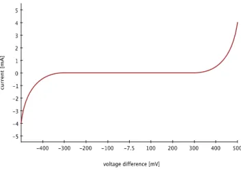
Fig 5 - Current voltage relation on a pseudo-resistor
The current-voltage relationship (Fig. 5) of the expansive element means that the effective resistance of the element is large for small signals and small for large signals. Therefore, the adaptation is slow for small signals and fast for large signals. The nonlinear variation of the resistance in the feedback loop means the transfer-function would not be permanent at the whole working period. If the cut of frequency is altered the whole distortion increases. This effect impairs significant in the lower frequency range (under 100 Hz).
- 8 -
There is a possible tradeoff between the noise and distortion. Using more pseudo resistor element in series helps decreasing the nonlinearity effect at the price of increasing noise figure. In this section, this tradeoff is analyzed on resistor-chains, which contain different number of pseudo resistor element. Because no one examined that before it leads me to a discovery what I write down as a thesis.
Fig 6 - Resistance variation at different number pseudo-resistor in series (curves PS2, PS8, PS16, PS32, PS64 respectively) [GΩ/V]
The series of pseudo-resistors results in decreasing distortion approximately linearly with the number of elements, due to the voltage different would be smaller between the two sides of each element (Fig. 6).
PS2
PS8
PS16
PS32
PS64
- 9 -
Fig 7 - Gated pseudo-resistance chain
It possible to give controllability to the resistance if we use switches to shortcut the remaining part of the chain (Fig. 7). This gated structure needs to be designed at least the required resistance plus the corner variations.
Note that the large number of the series connected pseudo resistor still does not have area large overhead neither the parasitic.
The switch implementation needs careful design as well. Large open state impedance is required so that they could be commensurable to the pseudo-resistances, otherwise the leakage will reduce the overall resistance;
hence they must be optimized to the OFF resistance oppositely the general usage.
S1 S2 S3
- 10 -
Design flow (1.2)
Fig. 8 - Design flow for the amplifier design
Creating a design flow (Fig. 8) can help us to design another bio-amplifier with different technology or specification. Based on the low frequency limit defined by the task specification we can calculate the required resistance value and also the ratio of the noise and distortion and number of pseudo- resistor. To determine the resistance of each pseudo element at first we need to calculate analytically the resistance from the BSIM3v3 transistor model parameters.
Technology
• size
• V
DD, V
T
• trans-impedance
• parasitic capacitances
• corner variability
Task specification
• cut-off frequencies
• A/D precision
max resistance
noise distortion
# of pseudo element transistor size
parasitic extraction switch
confidential factory parameters
- 11 -
= + +
+ + + + + + +
Self-compensation (1.3)
The next step was to find a quasi-automatic solution to get the required steady resistance value in normal operational condition. Even reduce resistance variations in different corner situations like the case of higher or lower temperature or supply voltage. The basic idea was to find a reference resistor with the same input and use a voltage difference with opposite sign to reduce or even extinguish the resistance variation effect.
Fig. 9a - Symmetry based double chain 9b - Current mirror controlled chain
The first solution (Fig. 9a) is a double chain where the master line length can be shortening if the voltage is dropped, so the resistance can keep the same level. It was the necessary to add comparators for the proper switching
- 12 -
and the higher default resistance to reduce the parallel connection.
The second version (Fig. 9b) based on current mirror, but operates the same way as the double chain. In the final design I had to implement many long transistors to reach the desired resistance to compensate the variation which lead to higher noise and current consumption.
Supplemented noise efficiency factor
The noise-power tradeoff is characterized by the Noise Efficiency Factor.
= ,
2 4
where νin,rms is the total equivalent input noise, BW is the -3 dB bandwidth of the amplifier, refers to the thermal voltage, and Itot is the average current consumption of each amplifier in the proposed architecture. The noise efficiency factor gives a good number to determine the connection between the noise and power consumption, but it doesn’t say anything about the distortion. If we take the maximal THD factor over the amplification range and convert to percent value, then we can multiply the NEF with it. With - 40dB distortion we got the same value as before.
= 20 max ( ) 100
- 13 -
Minimal noise CMOS and Bi-CMOS LNA array design (2)
To achieve the specification and get less than 1μV/√(Hz), it was necessary to do a comparison between the different technologies and architectures.
The amplifier had to be working in both the local field potential and the action potential range. In ordered to get the most usable signal the recording of the sub-hertz frequency was also necessary. To get a long time constant amplifier we used MOS pseudo-resistors. To avoiding the drawback of this solution, like the increased distortion, a chained series of these elements was used. It is inevitable to optimizing size and the number of the transistors in the chain, because increasing the number of element lead to decreasing the distortion and increasing the noise at same time. Figure 8 illustrate a basic design flow for the optimization. The used technology also specifies the limitation of the circuit. After the analyzing of the noise correspondence in different solution at the literature I decided the keep the design as simple as it possible to realize the smallest noise, that is shown in Figure 10.
- 14 -
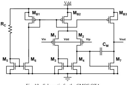
Fig. 10 - Schematic for the CMOS OTA
The M1-2 is the input transistor and M3-4 is the loading transistors. MBx are corresponding for the biasing and CM for the Miller compensation. The flicker noise is a general problem in a low frequency recording especially in LFP range. Over 100 Hz the thermal noise will be significant. To attenuate the noise, we examined the both the available CMOS and Bi-CMOS technologies. The bipolar transistors generate less flicker noise.
Unfortunately, the input resistors which has the largest impact in the noise have to be MOS type to get high input resistance. Commute only the loading MOS transistors with bipolar ones was not been enough. It was necessary to add another stage to avoid the reduced low-frequency gain by increasing the
Vdd
Vdd
Vin Vip
M1 M2 MB1
M7
M3 M4
M5 M6
MB2 MB3
Vout
RC
CM
- 15 -
input resistance of the second stage. The original amplification can be calculated: avdo = gm1(ro2||ro4||rπ7)gm7(ro7||rob3) If we exchange the load transistors (M3,M4,M7) than ro2,ro4 << rπ7 and avdo ≈ gm1rπ7 gm7(ro7||rob3) would be degraded. The Bi-CMOS solution gives higher unity gain and lower flicker noise, beside it occupies more area and it worse in thermal noise.
Fig. 11 - Schematic of the Bi-CMOS OTA
In order to design the lowest noise amplifier, it was needful to optimize the layout using interleaving, common centroid techniques and dummy transistors with precaution on symmetric placing and routing. For the larger size transistors with multiple fingers using the common centroid eventually
Vdd
Vdd
Vin Vip
M1 M2 MB1
Q1 Q2
M5 M6
MB2 MB4
Vout
RC
CM Q1
Q3 Q4 VSS VSS
MB3
VSS
M7 M8 Q5
Q6
- 16 -
rule higher noise. After the parasitic extraction the simulations indicated with the CMOS solution would guarantee better parameters. The experiments confirmed the results of the simulation. Using the same size of amplifiers, the CMOS solution generate lower noise. The chip was built with the AMS 0.35μm Bi-CMOS technology.
In the experiment the amplifier inputs connect directly to the neural probe, while the outputs connect to a distant external amplifier through 5m cable.
The standard deviation of the gain at the CMOS amplifier was 0.33dB and 0.26dB at the Bi-CMOS.
In conclusion, I report an ultralow noise CMOS and Bi-CMOS amplifier, which can be connected to neural probe. The Figure 12 and Table 1 shows the simulated and measured parameters for both types of amplifiers. The measured input referred noise was 670nV/√(Hz) with 22mHz cutoff frequency for the CMOS amplifier which is exceed our prior expectation.
- 17 -
Fig. 12 - The difference in noise simulation between CMOS and Bi-CMOS
Table 1 - simulated and measured (in brackets) parameters of the CMOS and BiCMOS LNA
Parameter CMOSLNA Bi-CMOSLNA
Supply Voltage 1.6 V 1.6 V
Process Technology 0.35 m Bi-CMOS 0.35 m Bi-CMOS
Midband Gain 40 dB 40 dB
-3 dB Bandwidth 53 (22) mHz ~ 10 (6) kHz 55 (30) mHz ~ 9.8 (6.5) kHz Input Referred Noise 610 (670) nVrms 777 (860) nVrms
Noise Efficiency Factor 4.4 4.2
THD -90 dB -94 dB
CMRR 39.6 dB 37.5 dB
PSRR 75.8 dB 77.2 dB
ICMR 2.36 V 1.92 V
Slew rate (1 mV input) 1.3 mV/s 1.5 mV/s
Power Consumption 240 W 220 W
- 18 -
Thesis 1
1.1
I proved that the generalized use of active pseudo resistors using extreme high-value resistors cannot be realized, which however is fundamentally important in the application of very low-frequency RC amplifiers’ feedback loop. The broadband behavior of pseudo resistors causes low frequency distortion which prevents accurate measurement. The analysis of these low frequency distortions in neural amplifiers that use pseudo resistance hasn’t been addressed before in the literature. [A1, A4]
1.2
I developed a design process for broadband extreme high-value and low distortion active resistors. The essence of the design process is the chaining of appropriately sized and suitably controlled pseudo MOS resistors, taking into account the scattered parasitic capacity, to minimize the distortion of the resistances and to optimize the noise in the system. [A1]
- 19 - 1.3
I developed two methods which are suitable for self-compensating the pseudo-resistance chains which were introduced in the previous (1.2) thesis point. The distortion caused by the active pseudo resistors can be further reduced using symmetry or current mirror based architectures. [A1]
- 20 -
Thesis 2
2.1
I developed a design procedure for high sensitivity neurobiological measurements, which with certain conditions such as allowed dissipation and size limits, achieves optimal input referred noise amplification with comparable noise and power consumption coefficient to other amplifiers for live animal measurements in laboratory. The architecture and the operation parameters were proved by measuring a chip manufactured by the Austrian Microsystems 0.35 µm stripe width Bi-CMOS technology. [A2, A3]
2.2
During the design process that was developed and described in thesis 2.1, I compared the low noise amplifier parameters using CMOS and Bi-CMOS technologies. The comparison proved that amplifiers fabricated on CMOS operate with less noise under similar size and power consumption. The tests chips were manufactured with the AMS 0.35 µm technology. [A2]
- 21 - 2.3
After examining the leading international journals with over two hundred articles published between 1997 and 2015 on the subject of neural signal low noise amplification, I concluded that, based on the published specifications for the technology I used, the amplifier implemented according to the established design method has better noise parameters.
[A2]
- 22 -
Author publications to support the thesis
[A1] Z. Karasz, R. Fiath, P. Foldesy, A. Vazquaez., “Tunable Low Noise Amplifier Implementation With Low Distortion Pseudo-Resistance for in Vivo Brain Activity Measurement,” IEEE Sensors Journal, vol. 14, no. 5, pp. 1357-1363, 2014.
[A2] Z. Karasz, P. Földesy, T. Molnar, I. Ulbert, “CMOS and BiCMOS Ultra Low Noise Amplifier array for brain signal measurement,“
Journal of Engineering, – release in progress (2016)
[A3] D. Gergelyi, P. Foldesy, Z. Karasz, C. Fuzy, “Serially connected MOS terahertz sensor array,” 38th International Conference of IEEE IRMMW-THz, pp. 1-2, 2013.
[A4] R. Carmona, A. Zarandy, P. Foldesy, J. Fernandez, Z. Karasz, M.
Suarez, T. Roska, A. Vazquez, “A hierarchical vision processing architecture oriented to 3D integration of smart camera chips,”
Journal of Systems Architecture, vol. 59, no. 10, pp. 908–919, 2013.
![Fig 6 - Resistance variation at different number pseudo-resistor in series (curves PS 2 , PS 8 , PS 16 , PS 32 , PS 64 respectively) [GΩ/V]](https://thumb-eu.123doks.com/thumbv2/9dokorg/1304163.104923/10.629.135.522.331.568/resistance-variation-different-number-pseudo-resistor-series-respectively.webp)