Proteins, polymers and living cells
on titanium oxide-based nanostructured coatings:
exploitation of label-free optical sensing methods
Ph.D. Thesis By:
Judit Nádor
Supervisors:
Róbert Horváth, PhD Péter Petrik, DSc
Institute of Technical Physics and Materials Science, Centre for Energy Research, Hungarian Academy of Sciences
Doctoral School of Molecular- and Nanotechnologies University of Pannonia
Head of School: Prof. Ferenc Vonderviszt, DSc
2016
DOI:10.18136/PE.2016.628
Proteins, polymers and living cells on titanium oxide-based nanostructured coatings: exploitation of label-free optical sensing methods
Értekezés doktori (PhD) fokozat elnyerése érdekében Írta:
Nádor Judit
Készült a Pannon Egyetem – Molekuláris- és Nanotechnológiák Doktori Iskolájában Témavezetők: Dr. Horváth Róbert, Dr. Petrik Péter
Az értekezést témavezetőként elfogadásra javaslom:
Dr. Horváth Róbert: igen / nem ………..
(aláírás)
Dr. Petrik Péter: igen / nem ………..
(aláírás) A jelölt a doktori szigorlaton ……… %-ot ért el.
Az értekezést bírálóként elfogadásra javaslom:
Bíráló neve: ………. igen / nem ………..
(aláírás)
Bíráló neve: ………. igen / nem ………
(aláírás) A jelölt az értekezés nyilvános vitáján ……… %-ot ért el.
………
Bíráló Bizottság elnöke A doktori (PhD) oklevél minősítése ………
………
EDT elnöke Veszprém,………..
Table of contents
4
Table of contents ... 3
Abstract (English) ... 6
Magyar nyelvű kivonat... 7
Abstract (Deutsch) ... 8
Abbreviations ... 9
1. Introduction ... 10
1.1. Morphology and applications of nanoparticles ... 12
1.2. Coating preparation procedures ... 16
2. State of the art... 18
2.1. Evanescent field-based sensing... 18
2.1.1. Optical waveguide lightmode spectroscopy ... 19
2.1.2. Surface plasmon resonance sensors ... 20
2.1.3. Grating coupled interferometry ... 21
2.1.4. Fiber-optic evanescent wave sensors ... 23
2.2. Ellipsometric methods ... 23
2.3. Surface micro- and nanostructuring ... 29
3. Motivation and aims ... 33
4. Materials and methods ... 35
4.1. Applied methods for the characterization of the solutions ... 35
4.1.1. Particle size distribution ... 35
4.1.2. Refractive index determination ... 36
4.2. Substrate preparation processes ... 37
4.2.1. Titanate nanotubes... 38
4.2.2. Titania nanoparticles ... 39
4.3. Sample solutions in the OWLS measurements ... 41
4.4. Sample solutions in the in situ ellipsometric measurements ... 42
4.4.1. Polyelectrolyte adsorption measurements ... 42
4.4.2. Protein adsorption and cell adhesion measurements ... 42
4.5. Applied microscopic methods ... 43
4.5.1. Atomic force microscopy ... 43
4.5.2. Digital holographic microscopy ... 44
4.5.3. Phase contrast microscopy... 45
4.6. Applied instruments for the coating characterization and the in situ adsorption experiments ... 47
4.6.1. Optical waveguide lightmode spectroscopy ... 47
4.6.2. Spectroscopic ellipsometry ... 47
4.7. Calculation methods in the adsorption measurements ... 47
5
4.7.1. Measuring principle of OWLS ... 47
4.7.2. The de Feijter formula ... 49
5. Results and discussion ... 50
5.1. Characterization of the coatings ... 50
5.1.1. Surface morphology and optical characterization of the coatings ... 50
5.1.2. Thickness characterization with spectroscopic ellipsometry... 52
5.1.3. Light-guiding capabilities of the TNT-coated OWLS chips ... 54
5.2. OWLS measurements on the TNT coatings ... 54
5.2.1. Protein adsorption on the TNT coating ... 55
5.2.2. Cell spreading kinetics and adhesion strength on the TNT coating ... 56
5.3. New time-sharing two-channel ellipsometric configuration and its applications in in situ adsorption measurements ... 62
5.3.1. The new setup and its advantages ... 62
5.3.2. The construction of the ellipsometric model ... 65
5.3.3. Polyelectrolyte deposition on the TNP coating... 69
5.3.4. Protein adsorption on the TNP coating ... 70
5.3.5. Ellipsometric experiment with living cells on the TNP coating ... 72
6. Summary and outlook ... 75
7. Thesis highlights ... 77
Tézispontok ... 80
8. List of publications ... 83
8.1. Publications related to the Ph.D. thesis ... 83
8.2. Oral and poster presentations related to the Ph.D. thesis ... 83
8.3. Other publications ... 85
9. Acknowledgements ... 86
10. References ... 87
6
Abstract (English)
The main topic of my doctoral work is nanostructured coatings made of titanium-oxide nanoparticles. Due to their advantageous biophysical properties, they are promising candidates for being applied as sensing surfaces on biosensors or as coatings on medical implants. In the first part of the dissertation I introduce titanate nanotube (TNT) thin films. The characterization of them was performed using atomic force microscopy, spectroscopic ellipsometry and optical waveguide lightmode spectroscopy (OWLS).
I demonstrated that OWLS sensor chips coated with these transparent nanostructured layers are still compatible with the OWLS device, the coating doesn’t quench the incoupling and the propagation of the light in the waveguide, the height of the resonant peaks doesn’t change considerably. I studied the adsorption of bovine serum albumin, and the adhesion of preosteoblasts and human embryonic kidney cells on the TNT coating. I revealed that the coating enhanced the adsorption of the protein, and the spreading and the strength of adhesion of living cells.
In the second part of my work I present a novel ellipsometric configuration in the Kretschmann geometry, with which the deposition of the sample can be studied in situ on two different surfaces simultaneously. While in this configuration the circumstances (temperature, humidity, sample concentration) are the same for the two measurements, the obtained results for the two surfaces can be compared in a more reliable way, than in the case of sequentially performed experiments.
Unlike conventional ellipsometric flow cells, multiple angles of incidence can be applied with this setup, due to the semi-cylindrical lens. The plasmon resonance, generated by a gold thin film on the substrate, improves the sensitivity of the measurements compared to previous configurations.
With this recently developed ellipsometric setup I carried out measurements in order to study the adsorption of polyelectrolytes, proteins, and living cells on surfaces coated with titania nanoparticles. I demonstrated that the coating significantly enhanced the adsorption of the proteins and the polyelectrolytes. The experiment with preosteoblasts showed, that the configuration is appropriate for studying living cells but for more exact evaluation further developments are necessary in model construction.
7
Magyar nyelvű kivonat
Doktori munkám központi témája titán-oxid alapú nanorészecskékből készített bevonatok, amelyek előnyös biofizikai tulajdonságaik miatt potenciálisan alkalmazhatók bioszenzorok érzékelőfelületeként, illetve orvosi implantátumok bevonataként. A disszertáció első felében titanát nanocsövekből készített rétegeket mutatok be, melyek karakterizálását atomi erő mikroszkóppal, spektroszkópiai ellipszometriai térképezéssel és optikai hullámvezető fénymódus spektroszkópiával (OWLS) végeztem.
Bizonyítottam, hogy az átlátszó nanostrukturált réteggel borított érzékelő chip alkalmas OWLS mérésekre, a bevonat nem rontja le a chip becsatolási és hullámvezetési tulajdonságait, a rezonanciacsúcsok magassága nem változik számottevően. A bevonatokon borjú szérum albumin fehérje, preosteoblast (éretlen csontképző) sejtek és humán embrionális vesesejtek kitapadását vizsgáltam. Megmutattam, hogy a bevonat elősegíti a fehérjék adszorpcióját és növeli a sejtek adhéziójának mértékét és erősségét.
Doktori munkám második részében egy olyan Kretschmann geometriájú spektroszkópiai ellipszometriai mérési összeállítást mutatok be, amellyel a vizsgált minta kitapadását egyszerre kétféle felületen, in situ tudjuk tanulmányozni. Mivel ebben az elrendezésben a két méréshez tartozó környezeti paraméterek (hőmérséklet, páratartalom, mintakoncentráció stb.) megegyeznek, a két felületre kapott eredmények összehasonlítása sokkal megbízhatóbbá válik, mint külön elvégzett kísérletek esetén. A korábbi ellipszometriai folyadékcellákkal szemben az üveg félhenger alkalmazásának köszönhetően több beesési szög alkalmazható, a hordozót borító arany vékonyréteg által létrehozott plazmon rezonancia pedig a módszer érzékenységét javítja a hagyományos ellipszometriai elrendezésekhez képest.
Az új mérési elrendezéssel titán-dioxid nanoszemcsékkel borított nanostrukturált felületen és arany kontrolfelületen végeztem adszorpciós kísérleteket polielektrolitok, fehérjék, valamint élő sejtek tanulmányozása céljából. A polielektrolitok és fehérjék esetében megmutattam, hogy a nanoszemcsés bevonatra nagyobb mennyiségű minta tapadt ki. Az élő sejtek vizsgálatával szemléltettem, hogy a mérési összeállítás alkalmas élő sejtek vizsgálatára, azonban a mérések pontosabb kiértékeléséhez további fejlesztések szükségesek a modellalkotás területén.
8
Abstract (Deutsch)
Das Hauptthema meiner Doktorarbeit ist die Herstellung verschiedener Schichten von Titan-Oxid Nanopartikeln. Durch deren vorteilhaften biophysikalischen Eigenschaften können diese Schichten als potenzielle Oberflächen von Biosensoren oder von medizinischen Implantaten verwendet werden. Im ersten Teil der Arbeit stelle ich die Dünnfilme von Titan-Nanoröhrchen (titanate nanotube - TNT) vor. Sie wurden mit Atomkraftmikroskopie, Spektralellipsometrie und OWLS (optical waveguide lightmode spectroscopy) charakterisiert.
Ich habe es demonstriert, dass die mit diesen nanostrukturierten transparenten Schichten bedeckte Oberfläche der Sensorchips mit dem OWLS-Gerät kompatibel ist. Der nanostrukturierte Dünnfilm löscht die Einkopplung und die Verbreitung in der Wellenleiter nicht, und die Höhen der Resonanzspitzen verändern sich nicht deutlich.
Ich habe sowohl die Adsorption von BSA (bovine serum albumin), als auch die Haftung von Preosteoblast und Nierenzellen auf TNT untersucht. Ich habe gefunden, dass der nanostrukturierte Dünnfilm die Adsorption von Protein und die Verbreitung und die Stärke der Haftung von lebenden Zellen erhöht hat.
Im zweiten Teil meiner Arbeit habe ich eine neue Konfiguration von Ellipsometrie in dem Kretschmann-Aufbau dargestellt, in dem die Adsorption gleichzeitig auf zwei unterschiedlichen Oberflächen untersucht werden kann. Da die Bedingungen (Temperatur, Feuchtigkeit, Konzentration) für beide Messungen gleich sind, können die Unterschiede zwischen den zwei Oberflächen einfacher bestimmt werden, als im Falle von nacheinander durchgeführten Messungen.
Mit konventionellen Flüssigkeitszellen verglichen, aufgrund des Aufbaus mit einem Halbzylinder können mit dieser Konfiguration Messungen von mehreren Einfallswinkeln durchgeführt werden. Die von einem Goldfilm erzeugte Plasmonenresonanz erhöht die Sensitivität der Messung gegenüber den vorherigen Konfigurationen.
9
Abbreviations
AFM atomic force microscope BSA bovine serum albumin
EMA effective medium approximation FGN fibrinogen
GCI grating coupled interferometry HEK human embryonic kidney MQ ultrapure milli-Q water MSE mean squared error
OWLS optical waveguide lightmode spectroscope PAH poly(allylamine hydrochloride)
PBS phosphate buffered saline PSS poly(styrene sulphonate) SEM scanning electron microscope QCM quartz crystal microbalance RIU refractive index unit
SE spectroscopic ellipsometer SPR surface plasmon resonance
TEM transmission electron microscope TNP titania nanoparticles
TNT titanate nanotubes
10
1. Introduction
In the last decades label-free, surface-sensitive methods became a key in various areas of biotechnological, biophysical and biological research. An important development of these techniques was the increased sensitivity, which made possible to detect very small concentrations of the target molecules. Due to the increased throughputs of these methods, they can now be applied with improved efficiency, even in basic biological research where good quality data with statistics is crucial. Furthermore, they became more user-friendly, thus no specific qualification is needed to employ them. The optical methods became especially successful, due to the non-invasiveness of specific spectrums of optical frequencies with biological samples and the low interference with disturbing electromagnetic radiation. In addition, they can operate without the application of any dye or labeling molecules, which could modify the target molecules or their environment and increase the costs and the complexity of the measurements.
I have started my Ph.D. research work in 2012 in the Nanobiosensorics and Ellipsometric Laboratories of the Institute of Technical Physics and Materials Science.
At that time several state-of-the-art techniques were available or were under development in these laboratories, such as optical lightmode spectroscopy, rotating- compensator ellipsometer, grating coupled interferometer or Corning Epic BT System.
These techniques were traditionally mainly applied to investigate thin films of proteins, lipids or polymers, but there is a general tendency in biosensor research to combine these technologies with living cells or even tissues. In order to keep up with current trends, we established the first cell culture biosensorics laboratory in Hungary, where the cultured cells can be studied with the above mentioned methods on an everyday basis, opening up new research directions in materials sciences, thus increasing the portfolio of our institute.
It is especially important nowadays to employ nanostructured functional materials in biosensing or in materials sciences in general. My work focused on additive-free, titanium oxide-based nanostructured layers and their integration in various biosensing methods in a simple way. I intended to make the first steps in the research of proteins and livings cells on these novel coatings and to demonstrate that the effects of the surface roughness on the analytes can be studied in a quantitative way using these techniques.
11
Nowadays nanotechnology plays a more and more important role, not only in the scientific but in our everyday life. With expanding toward the nanometer and subnanometer ranges, our knowledge and possibilities grow consumedly. Our electronic devices become more efficient and complex, new medications are being developed to cure the patients on cell- or molecular levels, engineers are capable to create materials with completely new or astonishing properties.
The word “nano” can be originated from the ancient Greek word ‘νᾶνος’ (nanos), which means dwarf [1]. Today it indicates the one billionth (10-9) of a unit in the metric system (Fig. 1.1).
Figure 1.1. Examples for objects in the micro- and nanoscale [2].
In the next chapters I give a brief overview of the most prevalent nanoparticles and their application possibilities, and the most known coating procedures.
12
1.1. Morphology and applications of nanoparticles
The criterion of a nano-object is to have a characteristic dimension in at least one direction lower than a few 100 nm [3]. Nanostructured materials can be categorized according to their dimensionality; there are zero-, one-, two- and three-dimensional nanostructures [4].
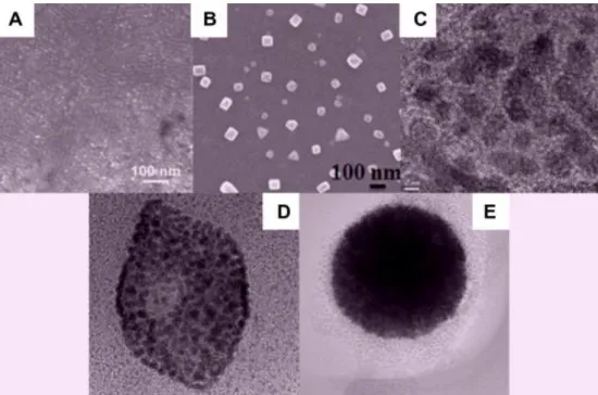
Zero-dimensional nanomaterials (Fig. 1.2) [4] have all their dimensions in the nanometer range. In this group we can find uniform particles arrays (quantum dots), heterogeneous particles arrays, core–shell quantum dots, onions, hollow spheres or nanolenses. Their synthetization can be very diverse, and they are performed by several research groups for a long time [5]–[8]. Zero-dimensional nanomaterials are primarily applied in solar cells [9], lasers [10], light emitting diodes (LEDs) [11], single-electron transistors [12], in diagnostics and in vivo imaging [13], optical sensing [14] and drug delivery [15].
Figure 1.2. Typical scanning electron microscope (SEM) and transmission electron microscope (TEM) images of zero-dimensional nanoparticles: (a) quantum dots, (b) nanoparticles arrays, (c) core–shell nanoparticles, (d) hollow cubes, and (e) nanospheres [4].
13
In the one-dimensional group of nanostructures (Fig. 1.3) [4], the particles have a significantly larger expansion in one direction, than in the other two. Nanowires, nanorods, nanotubes, nanobelts, nanoribbons, and hierarchical nanostructures belong to this assembly [16]–[20]. They are often applied as interconnects or as main units in electronic, optoelectronic, and electrochemical energy devices with nanoscale dimensions [4], in electrochemical biosensors [21], and medical applications [22].
Figure 1.3. Typical SEM images of different types of one-dimensional nanostructured materials: (a) nanowires, (b) nanorods, (c) nanotubes, (d) nanobelts, (e) nanoribbons, and (f) hierarchical nanostructures [4].
The two-dimensional nanomaterials (Fig. 1.4) [4] are plain structures and have one dimension which is considerably smaller than the others. This group includes nanoplates, nanosheets, nanojunctions (continuous islands), branched structures, nanoprisms, nanowalls, and nanodisks [23]–[27]. Today one of the most popular two-dimensional nanostructure is doubtlessly the graphene, but beyond it we can find other promising materials that can form monolayers, such as silicene, germanene, stanene, and phosphorene [28], [29]. These types of nanomaterials are widely studied and are hopeful candidates for being employed in electrical applications, like field-
14
effect-transistors or single-electron-transistors [30], [31], solar cells [32], or in highly efficient thermoelectric applications [29]. They are also popular in medical fields and were successfully applied in cellular imaging, drug delivery, gene delivery, tissue engineering [33], [34], and also in electrochemical and optical biosensors [35].
Figure 1.4. Typical SEM and TEM images of different types of two-dimensional nanostructures: (a) junctions (continuous islands), (b) branched structures, (c) nanoplates, (d) nanosheets, (e) nanowall, and (f) nanodisk [4].
The three-dimensional nanostructures (Fig. 1.5) can possess preferable properties over their bulk counterparts, due to their huge specific surface area [4]. The most typical three-dimensional nanostructures are nanoballs (dendritic structures), nanocones, nanocoils, nanoflowers and nanopillars [36]–[41]. The application possibilities of these three-dimensional nanostructures are very wide, so only a non-exhaustive list of examples is given here. Their unique properties can be exploited in electronic systems, like flexible solar cells [41], microfluidic devices with integrated electronics, chemical and biological sensors, or photonic and optoelectronic systems that combine unconventional materials with conventional silicon-based electronics [42] and rechargeable batteries [43], [44]. They can be applied in medicine as biomaterial scaffolds [45], in drug [46] and gene delivery [47], and in biological targeting [48].
15
Figure 1.5. Typical SEM and TEM images of different three-dimensional nanoparticles: (a) nanoballs (dendritic structures), (b) nanocoils, (c) nanocones, (d) nanopillars, and (e) nanoflowers [4].
Many types of nanoparticles from the above introduced groups could be exploited as surface coatings for various biosensing applications. When the aim is to determine concentration, affinity or adsorption of a target biomacromolecule (e.g., proteins), using label-free methods such as optical waveguide lightmode spectroscopy, spectroscopic ellipsometry or quartz crystal microbalance, the target objects are first required to be captured by a sensor. Therefore making the sensor surface as large as possible is beneficial, because more analytes can be captured. A popular method to accomplish that requirement and to improve adhesion is to nanostructure the surface which is accom- panied by the increase of the specific surface area [T1].
Another possible role of surface nanostructuring is that the changes of the surface roughness have an effect on the behavior of living cells (Fig. 1.6) [49]–[51]. Among other biophysicochemical properties of the substrate, like composition or topography, the surface roughness can be an effective tool in controlling cell adhesion, spreading or proliferation.
16
Figure 1.6. Cells on arrays of NSs. [52] A549 cell on silicon NSs (a) [53], HeLa cells on copper oxide NSs (b) [54], CHO or HeLa cell on hollow aluminum oxide NSs (c) [55], natural killer cell on silicon NSs (d) [56], cortical neuron cell on quartz NSs (e) [57], cortical neuron cell on a ring of platinum NSs (f) [58], T lymphocyte cells on silicon NSs (g) [59], retinal cell on gallium phosphide NSs (h) [60], and HEK293 cells on indium arsenide NSs (i) [52].
1.2. Coating preparation procedures
There are plenty of fabrication methods for preparing coatings. They can be classified in four general categories (Table 1.1), which are atomistic deposition, particulate deposition, bulk coating and surface modification [61]. In atomistic deposition processes, atoms are condensing onto a substrate surface and migrating to nucleation and growth sites to form the film. In this case the atoms can’t always reach their lowest possible energy configurations, therefore many structural imperfections (voids, dangling bonds, lattice mismatches) can be found in the resulting films. In particulate deposition
17
technologies solid or molten particles are used for depositing the coating, and the solidification and sintering steps are very important part of the method, which have a great effect on the resulting microstructure. Bulk coating processes require great amount of the coating material to be applied on the surface at once. In surface modification methods the surface composition or other properties are modified by chemical, mechanical, thermal or ion treatments [62].
Atomistic deposition Particulate deposition Bulk coating Surface modification
Vacuum environment
Evaporation
Molecular beam epitaxy
Ion beam deposition Plasma environment
Sputter deposition
Ion plating
Plasma polymerization
Glow discharge deposition
Electrolytic environment
Electroplating
Electroless deposition Chemical vapor
environment
Chemical vapor deposition
Spray pyrolysis Liquid phase epitaxy
Thermal spraying
Plasma spraying
Flame spraying
Detonation gun Fusion coating
Enameling
Electrophoresis
Wetting processes
Printing
Dip coating
Spin coating
Printing Cladding
Explosive
Roll-binding Weld coating
Chemical conversion
Anodic oxidation
Nitridation
Leaching Thermal surface treatment Ion implantation Laser glazing
Table 1.1. The classification of coating procedures [61].
18
2. State of the art
In this section I introduce the most important evanescent wave- and ellipsometry-based techniques. The last subsection is about surface structuring, which is often combined the highlighted novel technologies in order to improve the sensitivity of the method or the accessibility of immobilized receptors.
2.1. Evanescent field-based sensing
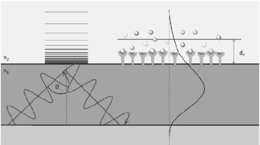
When an electromagnetic wave strikes an interface at an angle greater than the critical angle, it undergoes total reflection at the boundary, but a small part of the wave can penetrate into the adjacent medium. It generates the so-called evanescent field, which has an exponentially decreasing intensity orthogonally to the interface (Fig. 2.1). The evanescent field-based (bio)sensors utilize the fact, that the interaction or adsorption of (bio)molecules within the penetration depth (dp) of the evanescent field can cause the change of the effective refractive index for the guided mode and it leads to the change of the incoupling angle ().
Figure 2.1. The schematic image of evanescent field-based sensing. Total internal reflection and the evanescent wave penetrating into the adjacent medium (n2) with an exponentially decreasing intensity are represented. The interaction with (bio)molecules within the penetration depth (dp) of the evanescent field may lead to absorption or to a change of the effective refractive index for the evanescently guided mode [63].
19
2.1.1. Optical waveguide lightmode spectroscopy
Optical waveguide lightmode spectroscopy (OWLS) is a very popular label-free sensing method, where a dielectric waveguide layer forms the surface of the sensor chip (Fig. 2.2). It is based on the sensitive monitoring of refractive index changes near the surface, when the observed analytes (bacteria, proteins, cells etc.) are adsorbing onto the surface.
In the OWLS sensor chip there is a shallow surface grating in the planar waveguide, in order to excite the guided modes. The plane-polarized measuring light from the source (e.g., He-Ne laser) is diffracted from the grating and via total internal reflections it can propagate in the waveguide. At certain angles the numerous successive internal reflections will interfere and excite a guided mode. The light exits from the layer and is detected by photodiodes, placed next to the sensor. The light can be incoupled only at certain angles of incidence, and these angles are conditioned by various circumstances, for example the wavelength of the illuminating beam, the grating constant of the sensor, or the refractive index inside the evanescent field above the grating.
Figure 2.2. The schematic image of the measurement configuration of the optical waveguide lightmode spectroscopy [64]. Due to refractive index changes near the surface the incoupling angles are shifted, from which the adsorbed mass density can be calculated.
20
The changes of the refractive index in the evanescent field alter the conditions of the incoupling, which causes the change of the incoupling angles. During the measurement a high precision goniometer is rotating the sensor chip relative to the illuminating beam, and the incoupling angles can be determined from the positions of the sharp resonant peaks in the function of the measured light intensity and the angle of incidence. From the incoupling angles the effective refractive index and accordingly the adsorbed mass density of the studied objects (e.g. proteins, cells, bacteria) can be calculated [64], [65]
(see section 4.7, Eq. (3), Eq. (4), Eq. (5)).
The sensitivity of the OWLS can be as low as 10 pg/mm2 in adsorbed mass density or 3.4 × 10⁻⁵ RIU in refractive index [66] and its typical temporal resolution is around 2-20 s [67]. The commercially available standard OWLS sensor chips has coatings made of SiO2, TiO2, Ta2O5, ITO, ZrO2 or Al2O3 thin films, PTFE (polytetrafluoroethylene) or silicone thick films for passivation or APTES ((3- aminopropyl)-triethoxysilane) for silanization [68], but nanostructured sensor coatings are not available.
OWLS is widely used for studying surface processes in situ, especially in biological and medical fields, like the adsorption of proteins [69], living cells [70], [71] or bacteria [72] or it can be applied as immunosensor as well [73]. It is important to stress that optical waveguide-based sensors are now available in microtiter plate format (96, 384 wells) and successfully employed to monitor cell adhesion [74], [75], and cell signaling [76].
2.1.2. Surface plasmon resonance sensors
One of the most popular label-free optical biosensor is the surface plasmon resonance (SPR) sensor (Fig. 2.3). This method is based on the phenomenon, that when a conductor/dielectric material interface is illuminated by a light beam with specific wavelength in a specific angle, resonant oscillation of conduction band electrons occurs on the surface. Usually the exciting light is incoupled by a prism and undergoes total internal reflections from the interfaces of the conductor film, thus an evanescent field
21
will penetrate into the flow channel where the studied events (e.g. adsorption, capturing) are happening (see Fig. 2.3). The intensity of the detected light has minimum values at the angles and wavelengths where plasmon excitation happens, and from the changes of these parameters the mass of the adsorbed molecules can be calculated.
The sensitivity of the method is typically 10−5–10−8 RIU [66], [77]. SPR can be employed as a separate technique for detecting molecular adsorption, like protein, DNA or polymer adsorption, [78], [79], or it can be combined with other techniques (e.g.
Raman scattering [80], anodic stripping voltammetry [81], ellipsometry [82]) in order to enhance their sensitivity or provide complementary information.
Figure 2.3. A typical setup for a surface plasmon resonance biosensor [83]. The capturing of the target molecules on the sensor surface leads to changes of the angle of incident at which the plasmon enhancement happens.
2.1.3. Grating coupled interferometry
One of the most sensitive label-free biosensors on the market is the grating coupled interferometer [84], [85]. The sensing method (Fig. 2.4) is based on a planar optical waveguide sensor chip with two incoupling and one outcoupling grating. With an
22
expanded beam the two incoupling gratings are illuminated simultaneously, but one half of the beam is phase-modulated by a laterally divided two-cell liquid crystal modulator, in order to obtain the interference signal. The incoupled measuring and reference light beams interfere, and the third grating leads out the interference signal through an optical fiber to the detector. The studied phenomenon (e.g. protein adsorption) happens on the sensing surface between the two incoupling gratings, and alters the refractive index of the material in the evanescent field, thus the phase of the measuring beam will change compared to the reference beam. The surface sensitivity of this method was demonstrated to be below 0.1 pg/mm2 [85].
The GCI is ideal for measurements requiring high sensitivity and real time detection. A possible application can be in the field of fragment-based screening, where the interactions between receptors and very small (~100-200 Da) drug molecule fragments are investigated. The sensitivity of the GCI can be utilized for the detection of low concentration samples as well.
Figure 2.4. The working principle of the grating coupled interferometry (a) and the waveguide chip with the incoupled light between the second and the third gratings (b) [85].
23
2.1.4. Fiber-optic evanescent wave sensors
Evanescent waves can also be exploited in fiber-optic arrangements [86], [87], where a single optical fiber is applied as the sensor and also as the transmission line of optical signals. In an optical fiber a part of the light wave propagates in the core, but the 5-40%
of the total propagating power penetrates out of the fiber as an evanescent wave [88].
Optical fibers can be combined with surface plasmon resonance [89], [90], where the fiber is coated with thin metallic layer(s), and plasmon waves can be excited on its surface by the evanescent wave of the guided fiber mode. Resolution of 7×10⁻⁷ RIU was achieved by a multiple-peak SPR fiber-optic sensor [91], and sensitivity of 3161 nm/RIU was accomplished by applying metal-ZnO bilayers [92]. Another method was developed for increasing the sensitivity by replacing the standard polymer optical fiber with a three-layer structure in the sensing region to increase the intensity and the penetration depth of the evanescent wave. The new structure resulted a 3.91-fold improvement in the detection of the target antibody relative to a conventional sensor, and a lower limit of detection of 0.2 ng/L [93]. Fiber-optic evanescent wave sensors were successfully applied for detecting oligonucleotides [94], [95], antibody [93] or gas [89].
2.2. Ellipsometric methods
Ellipsometry is also a non-destructive label-free method, based on the phenomenon that if a light beam is reflected from an interface between two materials with different refractive indices, the polarization state of the light changes [96], [97]. There are numerous types of ellipsometers, but the most popular ones are the rotating-polarizer, the rotating-analyzer and the rotating-compensator ellipsometers.
The basic ellipsometric configuration (Fig. 2.5) is made up of two co-planar optical arms with adjustable included angle between them, and the controlling and processing electronic elements. One of the optical arms contains the light source and the polarizer, the other contains the analyzer and the detector. The compensator (optional) can be placed behind a polarizer or in front of an analyzer and it is employed to convert linear polarization to circular polarization and vice versa. After getting through the polarizer
24
the light beam becomes linearly polarized in the plane, which is determined by the actual state of the polarizer. Then the light reaches the sample and is reflected in a different (usually elliptically) polarized state. After getting through the analyzer the light beam becomes linearly polarized again and enters the detector [96].
Figure 2.5. Typical geometry of a rotating-compensator spectroscopic ellipsometry measurement with the indication of the angle of incident (Φa) and the polarization state of the measuring light beam [98].
In the case of a rotating-compensator ellipsometer, due to the continuously rotating compensator the detected intensity signal will have a sinusoidal shape. It can be Fourier analyzed to determine the ellipsometric angles Δ and Ψ (Fig. 2.6) defined from the ratio of the amplitude reflection coefficients for p- and s-polarizations (Eq. (1)). and Δ represent the changes in the ratio of the amplitudes and phase-shift between the two perpendicular (p- and s-polarized) components of the light during the reflection from the sample, respectively.
𝜌 = tan
𝑒𝑖𝛥 = 𝑟𝑝𝑟𝑠 Eq. (1),
where is the complex reflection coefficient, and Δ are the amplitude ratio and the phase difference between p- and s-polarizations, respectively and rp and rs are the amplitude reflection coefficients for p- and s-polarizations, respectively.
25
Figure 2.6. The schematic image of the principle of ellipsometry, demonstrating the ellipsometric angles (relative phase change) and Δ (relative amplitude change) [96].
Ellipsometry is an indirect method, which means that we can’t measure directly the data which we are interested in, like refractive index, surface roughness or layer thickness.
Instead, we must have some a priori knowledge about the structure of our sample, and have to set up an optical model based on that information (Fig. 2.7). Then the parameters of the optical model are varied (fitted) in order to make the experimental and calculated spectra overlap, which leads to the capability of reconstructing complex material systems, such as depth profiles [99], semiconductors [100], or three- dimensional protein structures [101].
26
Figure 2.7. The process of the ellipsometric data evaluation [102]. Using regression analysis, the hypothetic model is adjusted to find the requested parameters (e.g. optical constant, layer thickness) that generate data curves that best match the measured spectra.
The quality of the fit of the required parameters in the data evaluation can be determined by calculating the mean squared error (MSE) by the following equation:
MSE = √ 1
𝑁−𝑃−1∑ [(∆𝑖
𝑀−∆𝑖𝐶)2 𝜎Ψ𝑖𝑀 +(𝛹𝑖
𝑀−𝛹𝑖𝐶)2 𝜎Δ𝑖𝑀 ]
𝑁𝑖=1 Eq. (2),
where N is the total number of data points taken, P is the number of unknown (fitted) parameters, and Δ corresponding to the amplitude and phase change during reflection of polarized light from the sample surface, respectively. Superscripts M and C signify
“measured” and “calculated” data, respectively. If the MSE is around 1, the fit has a good quality. For more samples with more layers and complex structure, MSE values below 10 are acceptable.
The history of ellipsometry began in 1945, when the word ’ellipsometer’ was first used by Rothen, who applied the device to determine the thickness of barium stearate thin films deposited on metal slides [103]. Soon he used the ellipsometer for biological purposes; he studied films of antigens and antibodies on polished metal surfaces with a
27
sensitivity of ~0.3 Å [104], [105]. The following steps were the thickness measurement of unhydrated protein layers [106], and the development of the recording ellipsometer [107] and its combination with a cuvette, which makes possible to follow and record reactions (both adsorption and desorption) at solid-liquid interfaces continuously while the substrate is immersed in solution. It was employed for studying enzyme reactions, where proteins were applied as the solid substrate [108], [109]. With a similar recording ellipsometer blood clotting on tantalum-sputtered glass substrates was also studied [110].
In the middle of the 1970s the first spectroscopic ellipsometer was developed, which applied a spectral range from the near infrared to the near ultraviolet range [111]. Some years later an automated ellipsometer was introduced with unique properties of speed (1 measurement/2-3 s) and sensitivity (5 Å), making possible to follow biochemical reactions (e.g. protein adsorption, protein–protein interaction) at interphases with a high degree of accuracy [112]. The first ellipsometric studies related to the human body were the thickness measurements of the skin exposed to sunshine, and the investigation of the effectiveness of cosmetic products [113]. From the 1980s the biological studies carried out by spectroscopic ellipsometry became more and more popular. Adsorption kinetics and optical properties of various protein layers on different surfaces [114]–[117] were studied applying such devices. It was followed by the development of imaging ellipsometry, which can be applied for the quantification and the three-dimensional visualization of the lateral thickness distribution of transparent thin films on solid substrates with high layer thickness sensitivity (0.5 nm), high lateral resolution (5 μm) and high sampling speed (less than 1 s) [118].
In the same time the improvement of the surface plasmon resonance enhanced ellipsometry (also known as total internal reflection ellipsometry) also took place [119], [120]. A very good sensitivity can be achieved, if the conditions are appropriate for total internal reflection and surface plasmon effects are generated by employed thin metal films [121]–[123]. The advantages of this method can be exploited in many fields, such as in the characterization of fragmented antibody layers and estimating the orientation of antibody active sites from the experimental data [124], the detection of hazardous gas [125], [126] or low molecular weight environmental toxins, like simazine, atrazine and T2 mycotoxin [127], furthermore it can be combined with imaging ellipsometry [128].
28
Although, the first ellipsometric studies of cellular microexudates (also called cell coat materials) of different tissue cultured cells were published already in 1960 [129], [130], the first ellipsometric experiments with living cells were only performed a half century later. A surface plasmon resonance imaging ellipsometer was applied for studying adhesion properties and dynamics, cell-substrate and cell-cell interaction of different cell types [131]. Recently, the optical properties of mouse myoblast cells with different population densities were studied using spectroscopic ellipsometry [132].
In certain cases, it is beneficial to combine ellipsometry with other methods in order to get additional information about the studied object or phenomena. Two examples of these combinations and some examples for their applications are introduced below. The combination of ellipsometry and quartz crystal microbalance (QCM) is one of the oldest and most popular methods. The combination with grating coupled interferometry (GCI) is a very recent development, and its improvement is still in progress in our institute.
Quartz crystal microbalance enables label-free mass detection, based on measuring the frequency of a piezoelectric quartz crystal oscillator (Fig. 2.8). Due to small mass changes on the surface of the wafer the resonant frequency of the quartz is being altered, from which the surface mass density can be calculated. It is widely used as biosensor [133], it can be applied for studying living cells [134], aptamer-protein interactions [135], or for nucleic acid hybridization assays [136], [137].
Figure 2.8. The working principle of the quartz crystal microbalance [138]. The change in the mass (Δm) due to the adsorption of the monitored substance causes the change in the resonant frequency (Δf).
29
The first study in which ellipsometry and a quartz crystal microbalance were applied simultaneously was published in 1990. The complementary information received from the combination of the methods was used for the determination of the apparent density of the growing polyaniline thin film on an electrode surface sputtered onto the quartz crystal [139].
The buildup of polyelectrolyte multilayers was studied in situ with the combination of spectroscopic ellipsometry and quartz crystal microbalance with dissipation monitoring (QCM-D) in a single device. From the measured parameters the hydration of the polyelectrolyte multilayers could be calculated layer by layer [140]. In situ generalized ellipsometry combined with a similar QCM-D was applied for studying the deposition of engineered titanium dioxide nanoparticles on three-dimensional nanostructured slanted columnar thin films with controlled roughness [141].
GCI (see section 2.1.3) can also be combined in a single device with the spectroscopic ellipsometer, in order to exploit the high sensitivity of GCI and the spectroscopic capabilities of ellipsometry. Fibrinogen adsorption and layer-by-layer deposition of polyelectrolytes were studied so as to demonstrate the advantages of the combined device [142].
2.3. Surface micro- and nanostructuring
Micro- and nanostructured materials and surfaces got in the center of interest because of the remarkable novel properties (optical, catalytic, electronic, magnetic, ferroelectric or mechanical), which appear when the characteristic size of the material is reduced significantly [143]. In the 1960s the application of the first lasers [144] enabled the micropatterning of semiconductor surfaces with a characteristic size of around 2 m [145]. Later the development of various lithographic, deposition and surface modifying technologies induced the improvements in micro- and nanostructuring, such as achieving smaller and more controllable characteristic sizes [146], [147], higher aspect ratios [148], [149] or special surface properties [150], [151].
The behavior of different biomolecules on micro- or nanostructured surfaces started to be widely studied in the last decades, as novel biosensing techniques, medical implants
30
and biocompatibility, antibacterial and antifouling coatings are of great interest.The investigation of protein adsorption on a coating is essential in the field of implants, because the implant integration always begins with protein adsorption, cell adhesion happens subsequently. Hence the adsorption of proteins is a significant factor in determining the biocompatibility of a material [152].
Enhancing the protein adsorption can be beneficial in surface sensitive methods to increase the sensitivity of the biosensing device or on biomaterials to be implanted, in order to enhance advantageous cell adhesion and tissue responses. Some studies examined that beyond the increased surface area the microtopography [153] and nanotopography [154]–[157] of surfaces with the same chemical composition are also able to enhance the adsorption of proteins. Protein desorption promoting surfaces were also constructed by creating nano-scale superhydrophobic surfaces, which can be applied in microfluidic devices, where protein adsorption on the walls can cause problems [158]. In another study natural lotus leaves were applied as templates in replica molding in order to enhance the protein resistance and cell adhesion suppression of their antifouling coatings [159].
Since the failure of implants and prosthetic devices are often caused by bacterial infection, bacterial behavior is widely investigated on structured or patterned surfaces by various research groups. The morphological, genetic, and proteomic properties of adherent Escherichia coli bacteria were demonstrated to be altered by the different nanoroughness values of glass and gold surfaces [160]. The adhesion of Staphylococcus aureus and Escherichia coli was also studied on nanostructured silicon wafers with systematically varied, ordered surface topographies [161]. The same bacteria species were investigated on titania thin films with controlled and reproducible nanostructures.
The results revealed that bacterial adhesion and biofilm formation was affected by the nanoroughness in a non-monotonous way: the highest cell adhesion rate was observed on the surface with a roughness of 20 nm, and in the cases of smaller and greater roughness values the number of bacteria decreased [162].
In the case of studying the behavior of living cells an important role can be attributed to the surface topography. Intrinsically cell-repulsive hydrogels were turned into adhesion- and spreading-supportive surface for fibroblast cells by linear micropatterning in the presence of proteins [163]. Nanostructured platforms were fabricated from silicon by a
31
novel laser approach, and their functionalities were investigated using cervical cancer cells. The experiments revealed that the cancer cells couldn’t attach to the nanostructured patterns and started to migrate to untreated, flat areas [164]. Increased fibroblast response was observed on nanostructured polymer demixing of polystyrene and polybromostyrene compared to the flat surface. The cells showed gene up- regulation in the areas of cell signaling, proliferation, cytoskeleton, and production of extracellular matrix proteins [165].
Since titanium is very stable but light in weight, non-toxic material and it is not rejected by the body, it is widely used as dental or medical implants since the 1950s [166]–[168].
Therefore it is very important to emphasize the results of the studies about living cells on titanium- or titanium-oxide-based surfaces. There were (and still are) numerous in vivo animal experiments for testing titanium and titanium alloy implants, in order to reveal their physiological effects on the tissues [169]–[172].
From the 1970s the porous and the micro- or nanostructured titanium surfaces became popular biological and medical topics, and the greater part of the studies concluded consistently that structuring and increased roughness enhance the osseointegration and the bone regeneration [173]–[175]. In vitro studies also contributed to the better knowledge of how structured, rough surfaces affect the behavior of living cells, with special emphasis of osteoblasts and osteoblast-like cells. Numerous reviews were prepared about these topics [176]–[180], which concluded that surface topography has a great impact on the adhesion, proliferation, migration and other properties of living cells, however more detailed studies are needed to determine the correspondences between topography and cell behavior in a more exact way. Some examples of the most important studies are introduced below.
Different sizes (submicron to nanometer) of surface features and aligned patterns on titanium thin films were investigated and compared to flat titanium surfaces. The structuring was proved to be advantageous for cell adhesion for both endothelial and bone cells [181]. Micron and submicron structures were produced on titanium surfaces applying anodic oxidation and SaOS-2 human osteoblast-like cells were seeded on the surfaces. Enhanced cell adhesion and spreading were observed on the structured surfaces, and the results were explained by the phenomena, that porous structures can act as positive attachment sites for the filopodia of anchorage-dependent cells [182].
32
Fibroblast cells were studied on polished Ti-6Al-4V titanium alloy surfaces with 6 different average roughness values between 2.75–30.34 nm, and it was demonstrated that the roughness had a significant influence on the adhesion, proliferation and morphology of the cells [183]. Titanium substrates with rough and grooved surfaces were compared by culturing primary osteoblast-like cells on their surfaces. The grooved surface was demonstrated to enhance the cell attachment and proliferation compared to the rough surface [184]. Nanotubular titania surfaces were fabricated by a simple anodization process. In vitro measurements with marrow stromal cells and in vivo experiments with Lewis rats showed that the nanotubular surfaces enhanced the cell adhesion, proliferation and viability and did not cause adverse immune response [185].
33
3. Motivation and aims
In the first part of my work my aim is to prepare coatings from novel, additive-free titanate nanotubes on sensor chips, that are compatible with optical waveguide lightmode spectroscopic (OWLS) measurements and to apply them for various biosensing experiments. For the film fabrication I’m going to use the very simple and fast spin coating method. The nanostructured films have to be homogeneous and dense, but not too thick, because it could decrease the quality of the measurements. The required thickness would be between 5-15 nm, at which it is expected to well cover the surface, but doesn’t increase the optical thickness significantly.
I plan to characterize the micrometer-scale homogeneity of the coating with atomic force microscopy, and the millimeter-scale homogeneity and the film thickness with spectroscopic ellipsometry. The changes in the light guiding capabilities of the coated OWLS chip will be studied with the OWLS itself, by comparing the incoupling resonant peaks of the coated and uncoated sensor chips.
After the proper coating procedure is found, I would like to carry out protein adsorption and living cell adhesion measurements with the OWLS to study the effect of the coating. For the protein adsorption measurements I’m going to use bovine serum albumin and for the cell adhesion experiments I’m going to use human embryonic kidney cells and preosteoblasts. I also plan to incubate the living cells on coated and uncoated substrates for a longer time, and to monitor them with inverted microscopy and examine the effect of the coating on the behavior of the cells. I also would like to monitor these living cells on the nanostructured TNT coatings by a new digital holographic microscope, HoloMonitor M4. Therefore I plan to develop a new cuvette configuration that enables the long-term monitoring of living cells on spin-coated surfaces by the HoloMonitor.
In the second part of my work I’m going to take part in the development and the application of a new flow cell which can be instantly employed with the commercially available spectroscopic ellipsometers. This novel ellipsometric configuration can incorporate many advantageous properties of other conventional configurations, such as multiple angle of incidence, low sample consumption, in situ measurement, plasmon
34
enhancement and time-sharing two-channel monitoring. For the two-channel measurement, I intend to find a method to prepare substrates partially coated with titania nanoparticles. The untouched part of the gold surface can serve as the control in the measurements.
With the new configuration, at first I would study the layer deposition of polyelectrolytes on the nanostructured coating and on the uncoated surface. Afterwards I plan to carry out similar two-channel measurements with fibrinogen protein and preosteoblast cells and to reveal the effects of the coating on protein adsorption and cell adhesion.
35
4. Materials and methods
In this section I describe the methods and the materials that I applied in my experimental work, and give the types and operational details of the instruments I used.
First I introduce two techniques for characterizing the size distribution and refractive index of the sample solutions, then I specify the processes of substrate cleaning and coating. Later I give the details of solution preparation procedures for the different experiments, and I describe the applied microscopic methods. Finally I introduce the devices and calculation methods applied in the adsorption measurements.
4.1. Applied methods for the characterization of the solutions 4.1.1. Particle size distribution
Characterization of TNPs in ethanolic solution was carried out using dynamic light scattering (DLS) (Fig. 4.1) using a Malvern ZetaSizer NanoZS device. In the DLS measurements disposable plastic cuvettes with 500 μL solution were used. Three measurement cycles were carried out, and each cycle consisted of 10 measurements.
The wavelength of the laser in our instrument was 632.8 nm, and the data were collected at 20 °C.
DLS measurements are suitable for determining particle size distribution, molecular weight or zeta potential (electrokinetic potential in colloidal dispersions) for nanoparticles and colloid systems. When small particles are irradiated by a light with wavelength that is comparable to the particle size, the light scatters in all directions. The particles are undergoing Brownian motions and the distance between them is changing constantly, so the scattering intensity fluctuates over time. By analyzing these intensity fluctuations, the size of the particles can be concluded.
36
Figure 4.1. The schematic image of the theory of dynamic light scattering measurements with (a) larger and (b) smaller particles. Larger particles generates higher scattering intensity than smaller particles [186].
4.1.2. Refractive index determination
The refractive indices of the buffer and protein solutions were determined by a full automatic Rudolph J157 refractometer in order to use them in the evaluation process of the OWLS and ellipsometric measurements. The refractive index measurements were carried out at 20 °C and the wavelength of the measuring laser light was 632.8 nm.
The theory of operation of this device is based on that the direction of propagation of the light changes when the light beam passes through a boundary between two different materials with different refractive indices (Fig. 4.2). A light beam from a point source enters a prism with high refractive index, and bends when reaching the sample. Above a certain “critical” angle the bending becomes so great, that total reflection is occurred, so the light is actually reflected from the sample and through the prism it can reach the diode array detector. The transition from light to dark is detected and the refractive index can be calculated from that.
37
Figure 4.2. The working principle of the refractometer [187]. Above the critical angle the light is reflected from the interface and enters the detector.
4.2. Substrate preparation processes
I applied spin coating method (Fig. 4.6) for fabricating nanostructured coatings from sols containing titanate (H2Ti2O5 × H2O) nanotubes [188] or titania (TiO2) nanoparticles.
It is a reliable and reproducible method for rapid deposition of thin coatings on flat substrates [189], [190]. The substrate to be coated is held on a rotatable disc by vacuum, and before or during the spinning, the coating solution is dispensed onto the substrate surface. Due to the rotation the solution is spread out and generates the coating of the chosen material.
Figure 4.6. Schematic image of the spin coating procedure. The substrate is fixed on a rotatable disc and due to the spinning a uniform coating is composed from the dispensed solution.
38 4.2.1. Titanate nanotubes
The titanate nanotubes (TNTs) were synthetized using a previously reported protocol by László Kőrösi and his coworkers [188], our group received the ready-to-use TNT sols from them. These open ended nanoparticles have a diameter of 4-7 nm, and their length is around a few hundred nanometers (Fig. 4.7).
Figure 4.7. Transmission electron microscopic image of the titanate nanotubes (a) and the distribution of the diameter of the nanotubes (b) [188].
I prepared the TNT coatings on three different substrates: on OW2400 (Microvacuum Ltd.) Si0.6Ti0.4O2 optical chips for the OWLS measurements, on 1 × 1 cm pieces of silicon (1,0,0) substrates (covered by 3 nm thick native oxide) for the ellipsometric characterization and on microscope slides (MENZEL-GLÄSER, 1 mm thick, Thermo Scientific) for the AFM characterization.
The optical chips consist of a 0.5 mm glass substrate (n=1.53) and a ~200 nm waveguide layer with high refractive index (n=1.77). The incoupling of the laser beam into the waveguide layer is provided by a grating with 20 nm depth and 0.4166 μm periodicity. Before preparing the nanotube coatings on the optical chips, they were steeped in chromic acid (Merck) for 3 min, in ultrapure milli-Q water (MQ) for 2 s, in 0.5 M KOH solution (Merck, analytical grade) for 10 s and in MQ again. At last, the chips were sonicated in MQ water with an S 15 H Elma sonicator for about 30 min. The water was exchanged to fresh MQ water in every 3 minutes.
39
The Si plates were cleaned with hot ’Piranha solution’ (a 3:1 mixture of 95% H2SO4
(AnalaR NORMAPUR® ACS) and 30% H2O2 (Scharlab EMSURE® ACS)) for 15 min and subsequently profusely rinsed with MQ water.
The glass plates were steeped in Cobas Integra cleaner solution (300 mM HCl, 1%
detergent, Roche Diagnostics) and were sonicated for 15 minutes, then in water for another 15 minutes. Subsequently they were exposed to an O2 plasma (Plasma Prep II, Structure Probe Inc.) for 5 min.
The fast and simple spin coating procedure was carried out at room temperature on the three substrates, using a Convac St 450 spin coater. The spinning time was 20 s, the spinning speed was 3000 rpm and the volume of the dropped sol was 50 μL. After the substrates were drying for some minutes at room temperature, the highly transparent nanostructured coatings were ready to use.
4.2.2. Titania nanoparticles
The synthesis of titania nanoparticles (TNPs) and the sol preparation was also performed by László Kőrösi and his group, but so far no SEM or TEM images were taken of these nanoparticles. The preparation process was mostly similar to that described previously [188], [191], [192], except that in this procedure neither doping agents nor solvothermal treatment were applied. 50 mL of 2-propanol and 100 mL of distilled water was added to 13.3 mL of TiCl4, then 250 mL of 1.5 M NaOH solution was added dropwise to the solution during dynamic stirring. The emerging white precipitate was copiously washed with water and ethanol. Afterwards, dispersing ultrasonically the precipitate in ethanol, a stable dispersion of TNPs was formed. To obtain monodisperse nanoparticle mixture, the ethanolic dispersion was centrifuged at 12 000 rpm (13 225 × g) for 30 min, and then the separated supernatant with a solid content of 0.45 w/v% was used for the spin coating process.
I determined the size distribution of the TNPs in the ethanolic solution using Zetasizer Nano Zs (Malvern Instruments). The average size of the nanoparticles was found to be 11.34±1.97 nm.
40
The TNP coatings were applied in the in situ ellipsometric adsorption measurements, so I prepared them on specific substrates required by the ellipsometric configuration. The substrates were consisting of three layers: a cover glass, a 2 nm thick Cr2O3 layer, and a 20 or 30 nm Au layer. Cover glass slides coated with Cr2O3 and gold thin film by e-beam evaporation were purchased from Optilab Ltd., Hungary. Prior to the spin coating of the TNPs, the substrates were rinsed with MQ water, then steeped in methanol (VWR Chemicals) and acetone (VWR Chemicals) for 10 s each. The substrates were dried with nitrogen gas between and after the cleaning steps.
The parameters of the spin coating procedure were the same as described for the TNT coatings, but additional steps were needed to create partially coated substrates for the multichannel in situ ellipsometric measurements. First I wrapped one half of the sample surface with a specific stick-on foil (Wafer Tape SWT 10+R) before spin coating the TNPs on it. The spinning time, the spinning speed and the volume of the dropped sol were the same as in the previous procedures. The spin coating was followed by the removal of the foil with the TNPs on it, thus half of the substrate surface remained clean and uncoated.
It was verified by the ellipsometric measurements performed on the uncoated part of the surface before and after the application of the foil. Several samples were measured before and after the foil application and the spectra within the wavelength range of 400-1700 nm were compared (Fig. 4.8). The average difference between the ‘before foil’ and ‘after foil’ states was 0.08° for Ψ and 0.34° for Δ, which is equivalent to ca.
0.2 nm change in roughness, which can be considered negligible and can also be the result of the poor reproduction of the measuring position on the substrate.
![Figure 1.3. Typical SEM images of different types of one-dimensional nanostructured materials: (a) nanowires, (b) nanorods, (c) nanotubes, (d) nanobelts, (e) nanoribbons, and (f) hierarchical nanostructures [4]](https://thumb-eu.123doks.com/thumbv2/9dokorg/872166.46909/13.892.185.751.357.724/different-dimensional-nanostructured-materials-nanowires-nanoribbons-hierarchical-nanostructures.webp)
![Figure 1.4. Typical SEM and TEM images of different types of two-dimensional nanostructures: (a) junctions (continuous islands), (b) branched structures, (c) nanoplates, (d) nanosheets, (e) nanowall, and (f) nanodisk [4] .](https://thumb-eu.123doks.com/thumbv2/9dokorg/872166.46909/14.892.174.761.295.621/different-dimensional-nanostructures-junctions-continuous-structures-nanoplates-nanosheets.webp)
![Figure 1.5. Typical SEM and TEM images of different three-dimensional nanoparticles: (a) nanoballs (dendritic structures), (b) nanocoils, (c) nanocones, (d) nanopillars, and (e) nanoflowers [4]](https://thumb-eu.123doks.com/thumbv2/9dokorg/872166.46909/15.892.184.751.105.445/different-dimensional-nanoparticles-nanoballs-dendritic-structures-nanopillars-nanoflowers.webp)
![Figure 1.6. Cells on arrays of NSs. [52] A549 cell on silicon NSs (a) [53], HeLa cells on copper oxide NSs (b) [54], CHO or HeLa cell on hollow aluminum oxide NSs (c) [55], natural killer cell on silicon NSs (d) [56], cortical neuron cell](https://thumb-eu.123doks.com/thumbv2/9dokorg/872166.46909/16.892.159.778.113.614/figure-cells-arrays-silicon-aluminum-natural-silicon-cortical.webp)
![Figure 2.2. The schematic image of the measurement configuration of the optical waveguide lightmode spectroscopy [64]](https://thumb-eu.123doks.com/thumbv2/9dokorg/872166.46909/19.892.147.780.675.1008/figure-schematic-measurement-configuration-optical-waveguide-lightmode-spectroscopy.webp)
![Figure 2.4. The working principle of the grating coupled interferometry (a) and the waveguide chip with the incoupled light between the second and the third gratings (b) [85]](https://thumb-eu.123doks.com/thumbv2/9dokorg/872166.46909/22.892.307.637.618.1056/figure-working-principle-grating-interferometry-waveguide-incoupled-gratings.webp)
![Figure 2.5. Typical geometry of a rotating-compensator spectroscopic ellipsometry measurement with the indication of the angle of incident (Φ a ) and the polarization state of the measuring light beam [98]](https://thumb-eu.123doks.com/thumbv2/9dokorg/872166.46909/24.892.148.786.292.552/typical-compensator-spectroscopic-ellipsometry-measurement-indication-polarization-measuring.webp)
![Figure 2.6. The schematic image of the principle of ellipsometry, demonstrating the ellipsometric angles (relative phase change) and Δ (relative amplitude change) [96]](https://thumb-eu.123doks.com/thumbv2/9dokorg/872166.46909/25.892.221.707.108.414/schematic-principle-ellipsometry-demonstrating-ellipsometric-relative-relative-amplitude.webp)
