Surface & Coatings Technology 421 (2021) 127433
Available online 18 June 2021
0257-8972/© 2021 The Authors. Published by Elsevier B.V. This is an open access article under the CC BY license (http://creativecommons.org/licenses/by/4.0/).
The growth of a multi-principal element (CoCrFeMnNi) oxynitride film by direct current magnetron sputtering using air as reactive gas
G. Radn oczi ´
a,*, R. Dedoncker
b, G.Z. Radn ´ oczi
a, Zs. Czig ´ any
a, A. Sulyok
a, V. Kov ´ acs-Kis
a,c, D. Depla
baCentre for Energy Research, Konkoly-Thege M. u. 29-33, Budapest H-1121, Hungary
bDepartment of Solid State Sciences, Ghent University, Krijgslaan 281(S1), Gent 9000, Belgium
cInstitute of Environmental Sciences, University of Pannonia, Egyetem str. 10, Veszpr´em H-8200, Hungary
A R T I C L E I N F O Keywords:
CoCrFeMnNi MPEA Growth in Ar +air plasma MPEA-oxynitride Stochastic structure Spinodal decomposition Structure formation mechanism
A B S T R A C T
CoCrFeMnNi multi-principal element alloy films were grown by direct current magnetron sputtering in a mixture of argon and air. The air fraction was varied from 4 to 50%, which resulted in a change of the phase state of the growing film. A 〈100〉preferred orientation face centered cubic metal (doped with O and N) structure develops below 12% of air. Between 12 and 30% air, a two phase 〈100〉preferred orientation face centered cubic metal + oxynitride (B1) structure forms. Above 30% of air a single phase B1 oxynitride structure is observed. Compared to nitrogen, oxygen is preferentially incorporated into the growing structures. The 〈100〉preferential orientation is the result of selective nucleation (below 30% of air) or competing growth (above 30% of air) of the forming crystals.
Detailed microscopic analysis shows a complex structure for both the metal and the oxynitride phase in the films deposited at low and high air fraction. In both cases, the films are characterized by local structures ordered on a few nanometer scale and their formation is explained as a result of spinodal decomposition of the as-formed homogenous structure which occurs during film growth.
1. Introduction
Multi-principal element alloys (MPEAs) are a class of alloys that are composed of several elements in near-equimolar concentrations. The field of MPEAs was discovered about 15 years ago but still holds many interesting features. Against the intuitive expectation, some of these compositionally complex alloys have a simple crystallographic structure such as a face centered (fcc) or body centered cubic (bcc) structure with the constituent elements randomly distributed over the lattice positions [1–3]. When some specific requirements are reached, these materials can also be labelled high entropy alloys [4]. These materials received already much interest due to their excellent mechanical behavior as bulk material, but in thin film form many aspects remain undiscovered.
Especially, research on compound thin films based on MPEAs holds a vast uncharted territory. Magnetron sputtering is the method of choice to deposit multiple elements simultaneously. Not only the flexibility and tuneability of this physical vapor deposition technique makes it an attractive choice, but also the high quenching rate makes the technique
especially suited for deposition of MPEAs, as it favors the formation of a solid solution. From literature and previous studies, it became clear that nitrides and oxides of MPEAs also show the same remarkable structures when they are deposited by magnetron sputtering. In the case of the CoCrCuFeNi alloy, the addition of nitrogen or oxygen to the discharge resulted in the same B1 (NaCl) structure [5–8]. This intriguing similarity triggers the interesting fundamental question whether this behavior can be extended to a mixture of oxygen and nitrogen, and how both gases influence the structure development during thin film growth. While the number of the papers related to metal multicomponent alloys grown by DC sputtering in Ar/O2 or Ar/N2 gas mixtures is quite numerous, there is less information about the films grown in argon/air mixtures or in pure air [9–10]. Films grown with the addition of air or in pure air, are re- ported to be amorphous [9] or nanostructured single phase CrMnFeCoNi oxynitrides [10,11]. In [10] a porous film consisting of few nanometer sized grains (fcc structure, 0.4242 nm lattice parameter) was observed.
In this paper, a detailed atomic level structural analysis of CoCr- FeMnNi oxynitride thin films is performed. The goal is to get insight into
* Corresponding author.
E-mail address: radnoczi@mfa.kfki.hu (G. Radnoczi). ´
Contents lists available at ScienceDirect
Surface & Coatings Technology
journal homepage: www.elsevier.com/locate/surfcoat
https://doi.org/10.1016/j.surfcoat.2021.127433
Received 3 May 2021; Received in revised form 11 June 2021; Accepted 12 June 2021
the atomistic processes responsible for the growth mechanism and the morphological development of the film structure. Nevertheless, some general considerations can already be made at this point. These con- siderations also include the necessary terminology used further in the paper.
In multicomponent oxides, nitrides and oxynitrides with a B1 lattice the individual unit cells in a crystal will be different when more than 5 elements are present. This inevitably involves that translational sym- metry of such a crystalline structure will be only statistically valid.
Hence, nano-scale fluctuations of the elemental composition will occur.
Moreover, more complex structural changes at the same level are also expected because each of the constituent elements can have a different chemical affinity towards the other components. These fluctuations originate from the simultaneous formation of (metastable, or even un- stable) phases with a similar formation energy. The aforementioned fluctuations are known as stochastic fluctuations and are connected to the atomic structure of the material and/or processes taking place dur- ing growth [12]. These homogeneity fluctuations, due to positioning/
distribution of the composing atoms, are not the only possible kind of variations in the structure. Indeed, it is possible that not atoms, but rather structural units built up from several atoms can be the building blocks. When these structural units are arranged in a random or an or- dered way, different from the parent structure, the changes are char- acterized and discussed by a model known as the Rigid Unit Mode (RUM) model [13]. The discussed structural variations (stochasticity and RUM) can give a framework for the description of the nanostructure of the MPEA films and their oxides, nitrides or oxynitrides. A funda- mental question is, how these structural variations can emerge during thin film growth. It can be assumed that the growing films should be inherently homogeneous due to the high super cooling, negligible driving forces to decomposition and low mobility during growth.
However, this presumption does not exclude short range atomic rear- rangements and diffusionless processes. Consequently, as grown or even still growing films can undergo structural changes under the very limited kinetic conditions when diffusion is limited to several atomic distances. An example of such mechanism is spinodal decomposition as already observed in AgCu alloy films and particles [14,15].
This paper discusses the deposition conditions, the X-ray diffraction (XRD) analysis and, for a selected number of samples, a detailed trans- mission electron microscopy (TEM) study of (CoCrFeMnNi) oxynitride thin films. The above given considerations will then be confronted with these experimental results to provide a better insight in the growth mechanism and the morphological development of the deposited films.
2. Experimental
Depositions were performed in a home-built stainless steel vacuum chamber. A background pressure of less than 4.10−4 Pa, as measured with a Penning gauge (Compact Full Range gauge, Pfeiffer Vacuum), was achieved by the combination of a rotary pump and a turbomolecular pump. A CoCrFeMnNi powder target was made according to a procedure described elsewhere [16–19]. Prior to plasma discharge, argon and dry air, i.e. a 20/80 mixture of oxygen and nitrogen, was introduced by two mass flow controllers (MKS instruments) to reach a total pressure of 0.5 Pa at a total flow rate Qtot of 20 sccm. The fractional flow rate of air is calculated as RON =QON/(QON +QAr) =(QON/Qtot) where QON and QAr
represent the air and argon flow, respectively.
The samples were deposited at room temperature on a Si [100]
substrate with a native oxide, cleaned according the Radio Corporation of America procedure. The substrate was placed at a distance of 63 mm from the target. All depositions were executed at an average deposition rate of 1.5 nm/s, a discharge voltage around 530 V and at a constant discharge current of 0.3 A. As the air flow was increased, the deposition rate and discharge voltage decreased slightly. The time of deposition was adjusted to achieve films with a thickness between 1 and 2 μm.
XRD patterns were collected from a Bruker D8 Discover (with a
LynxExe silicon strip detector and CuKα radiation) in Bragg-Brentano configuration. All samples were scanned from 20◦to 100◦with a reso- lution of 0.02◦per step of 1 s. The chemical composition was measured by a combination of energy dispersive spectroscopy (EDS) (metals) and wavelength dispersive spectroscopy (WDS) (O and N). EDS was per- formed on a FEI Quanta 200F electron microscope. The spectra were analyzed with EDAX Genesis software. The WDS analysis was performed on a JEOL JXA-8530F.
The X-ray photoelectron spectroscopy (XPS) analysis was carried out under ultrahigh vacuum conditions (2 × 10⁻⁹ mbar). The specimens were exposed to 70 ◦C heat treatment for 48 h, which is the standard baking procedure of the applied vacuum system. The surface of samples was cleaned by ion sputtering to remove the contamination from air and to fully remove the surface oxidized range.
The following conditions for the ion sputter cleaning were used: 1 keV Ar ions bombarding the sample at an angle of 80o measured from the surface normal. The specimen was rotated during the cleaning procedure. The photoelectron spectra were obtained using X-ray radia- tion (Al anode with water cooling, 15 keV excitation). The XPS mea- surement yielded information of the average surface composition of an area of approximately 5 mm diameter. Constant energy resolution of 1.5 eV was provided by a special cylindrical mirror analyzer with retarding field (type DESA 150, Staib Instruments Ltd). All spectra were recorded with 0.1 eV energy steps. The following peaks were used for evaluation:
O 1 s (532 eV), N 1 s (399 eV), Ni 2p 3/2 (853 eV), Co 2p 1/2 (794 eV), Fe 2p 1/2 (720 eV), Cr 2p 1/2 and 3/2 (584 and 574 eV), Mn 2p 1/2 (650 eV). Although the XPS analysis of major components of a homo- geneous material is a standard procedure, in this case it was a difficult task because of the fact that contributions (XPS peak, Auger peak, loss peak) of these 3d elements either overlap or are located close to each other which prevents the separation of the elemental contribution of the main peaks. This circumstance made us to use the 2p 1/2 peak instead of the usual 2p 3/2 peak for quantification of Mn, Fe and Co, as listed above. As a result, the quantification was difficult and resulted in a large error, especially when determining the metallic and compound fractions of metal components. Concentration calculations were performed assuming homogeneous model with sensitivity factor from [20].
From a series of depositions performed at different fractional air flows, four samples, grown with 12, 20, 30 and 50% air fraction in the sputtering gas, were chosen for TEM analysis. Structural investigation was carried out by cross sectional TEM and high resolution electron microscopy (HREM). Sample preparation for electron microscopy was made by FIB (Thermo Fisher Scios 2 dual beam) applying 2 kV Ga ions in the end of the procedure to reduce the caused damage. For TEM analysis a Philips CM20 and a FEI Themis 200 G3 transmission electron micro- scope with a Cs corrected objective lens in both HREM and scanning transmission electron microscopy (STEM) mode was used, both operated at 200 kV. EDS analysis was performed to verify the composition of the samples (Themis Super-X EDS detector). For EDS quantification the background was determined using parabolic multi-polynomial model.
The background windows were chosen automatically by the software (Velox 2.10) and then checked visually on the spectrum if any manual corrections were needed. For quantification of the peaks the Brown- Powell ionization cross section model was applied. Absorption correc- tion was applied supposing 70 nm as a reliable thickness of the FIB lamella and a density of 8 g/cm3. For a reliable comparison of TEM-EDS data, special care was taken to use the same experimental conditions and fitting procedure for the measured samples.
3. Results
3.1. X-ray diffraction analysis
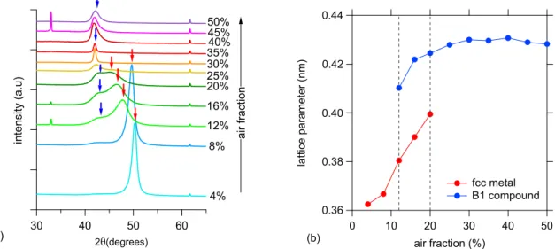
To map the structure of the films, grown at different air fractions in the discharge gas, X-ray diffraction patterns were recorded (Fig. 1). At low air fractions (4 and 8% air) only one diffraction peak (a single phase
structure) is observed. Fig. 1b shows the change of the lattice parameter as a function of the air fraction flow ratio. For this phase, the increase in the lattice parameter (0.36–0.39 nm), compared to CoCrFeMnNi alloy grown in pure Ar (a = 0.358–0.360 nm) [8,21] is attributed to the incorporation of dissolved oxygen and nitrogen.
For the films deposited in 12% or 20% air, a very broad double peak is recorded, each of them is identified as a 200 reflection, revealing a two phase structure in this interval. The phases are attributed to an oxygen/
nitrogen doped fcc metallic CoCrFeMnNi phase and a B1 type CoCrFeMnNi-oxynitride phase with a lattice parameter of approxi- mately 0.43 nm [10].
For the film deposited at an air fraction of 30%, a single, sharp XRD 200 peak (Fig. 1) is observed which indicates large coherently scattering
regions and a single phase oxynitride structure as well. A further in- crease of the air fraction results in the broadening of the 200 peak which is at least twice as broad in the case of the 50% air sample as in the case of the 30% air sample. For the samples deposited at an air fraction equal or higher than 40% we observe an asymmetry in 200 peak. Further investigation is required to elucidate this effect. The 200 XRD peak of films from 25% air is of very low intensity compared practically to the peaks of all samples, grown below 25% air in the sputtering gas (Fig. 1).
As the X-ray diffraction patterns were recorded in Bragg-Brentano geometry, the observation of only one 200 peak can be interpreted as a strong 〈100〉preferred orientation, formed during the growth of both phases.
60 50
40 30
2 (degrees)
4%
12%
8%
16%
20%
25%
30%
35%45%50%40%
(a)
0.44
0.42
0.40
0.38
0.36
lattice parameter (nm)
50 40 30 20 10 0
air fraction (%) (b)
fcc metal B1 compound
air fraction
intensity (a.u)
Fig. 1. (a) XRD θ-2θ pattern of CoCrFeMnNi films grown in Ar +air sputtering gas. All films have a strong 〈100〉preferred orientation. Note the shift of the fcc 200 peak to smaller 2θ angles, i.e. larger d spacing, from 4 to 20 air % in the sputtering gas. From 12% the appearing second peak corresponds to the 200 peak of the B1 oxynitride phase. The XRD patterns have been vertically shifted for clarity. The two small peaks at 33◦and 61.7◦can be attributed to the Si substrate. (b) The lattice parameter as function of air fraction in the sputtering gas for the two detected phases. The figure reveals two single phase regions (below 12% and above 20% of air), separated by a two phase region.
Table 1
Chemical composition of the different samples. The light gray rows refer to the composition as measured with EDS on thinned samples for TEM analysis. The dark gray rows are measured by XPS analysis. All other compositions were measured with a combination with EDS (metal) and WDS (O and N).
Elemental composition, at. %
Air% Method N O Cr Mn Fe Co Ni
4 EDS/WDS 5.2 7 19 13.6 19.6 18.7 16.9
8 EDS/WDS 7.4 6.9 18.2 13.5 18.9 18.4 16.7
12 EDS/WDS 9.3 7.5 17.5 13.2 18.2 18.1 16.2
EDS(TEM) 15.9 ±1.5 15.1 ±3.4 15.0 ±2.4 10.7 ±1.8 15.5 ±2.5 15.1 ±2.5 12.6 ±2
16 EDS/WDS 10.2 7.3 17.2 12.9 18.2 18.1 16.1
18 EDS/WDS 12.1 9 16.6 12.4 17.5 17.3 15.3
20 EDS/WDS 11.7 7.7 16.7 12.6 17.9 17.7 15.7
EDS(TEM) 16.1 ±1.6 17.9 ±3.9 14.1 ±2.3 10.4 ±1.7 14.9 ±2.4 14.3 ±2.3 12.2 ±2
XPS (all) 14.0 ±1.5 18.6 ±2.0 14.2 ±1.5 11.7 ±1.5 16.6a ±2.0 14.8 ±1.5 10.1 ±1.0
XPS (metal) 7.4 ±1.5 3.7 ±1.5 a 9.4 ±1.5 9.1 ±1.5
XPS (comp) 6.8 ±1.5 8.0 ±1.5 a 5.4 ±1.5 1a ±1
22 EDS/WDS 13.1 10.2 15.8 12 16.5 17.4 15
25 EDS/WDS 12.6 13 15.5 11.9 16.2 16.3 14.5
30 EDS/WDS 4.9 27.7 13.1 8.9 15.1 16.6 13.6
EDS (TEM) 4.9 ±3 44.6 ±11 9.2 ±2 7.2 ±2 11.5 ±2 12.0 ±2 10.7 ±2
35 EDS/WDS 4.4 28 12.9 9 15.3 16.4 14.1
40 EDS/WDS 4.4 29.1 11.6 8 15.8 16.6 14.5
45 EDS/WDS 3.6 30.3 11.1 7.7 15.5 17.1 14.7
50 EDS/WDS 3.1 30.2 10.9 7.8 15.8 17.8 14.5
EDS (TEM) 8.0 ±3 41.6 ±10.7 8.1 ±2 7.9 ±2 11.9 ±2 12.3 ±2 9.9 ±2
XPS (all) 2.7 ±0.5 56.5 ±8 8.6 ±2 7.5 ±2 9.3 ±2.5 7.1 ±2 8.3 ±2
XPS (met) 1.0 ±2 0 ±2 a 3.7 ±2 1.6 ±2
XPS (comp) 7.6 ±2 7.5 ±2 a 3.4 ±2 6.7 ±2
aDue to evaluation difficulties only very approximate values are available.
3.2. Chemical composition
The chemical composition of the films was obtained by three different methods. In a first analysis, all samples were measured by a combination of WDS and EDS (see Table 1). As a second approach to access the chemical composition, EDS on the thin samples, prepared for the structural analysis by TEM (see further) was used. Finally, the composition of the samples was measured by XPS. Table 1. shows the results of the measurements for all samples, the four samples measured by TEM +EDS are marked by light gray background. From all data sets it is observed that though the quantity of oxygen in the sputtering gas is four times less than the quantity of nitrogen, oxygen is preferentially incorporated into the growing films.
In the films deposited between 4 and 25% of air, the quantity of the incorporated oxygen and nitrogen is practically the same, while from and above 30% air in the sputtering gas, basically oxygen is incorpo- rated and the quantity of incorporated nitrogen is much lower. It is also evident from Table 1 that in the case of 12% and 20% air the incorpo- rated anion concentration (O +N) is capable of bonding about 2/5th of the metallic ions to form a B1 (NaCl) type lattice. On the contrary, in the films grown at 30% air and higher air fractions in sputtering gas the anion quantity is sufficient to chemically bond all metal atoms in the structure. Elemental composition profiles of the samples were also measured by EDS/TEM (see Fig. A1 (Appendix)). All components are distributed uniformly in the films, showing only fluctuations of the order of the measurement error in Table 1.
As a final method, XPS was performed on two samples (see Table 1, dark gray rows). The XPS measurements support the EDS/WDS results
and give a reliable estimate on the anion to metal ratio in the films.
Difficulties of the quantitative evaluation of the XPS results origi- nated from the large number of overlapping XPS and Auger peaks for elements in different binding states. The chemical composition of the 20% and 50% air samples was measured and fractions of compound and metallic bonded components were estimated. The nitride and oxide bonds were not distinguished but the built-in nitrogen/oxygen ratio can be a guide for their quantity. According to the XPS measurements, in the 20% film the amount of oxygen atoms (and thus the oxide compounds) somewhat exceeds the nitrogen quantity despite the one-to-four oxygen to nitrogen ratio in the sputtering gas. The oxygen and nitrogen contents in the 20% sample practically correspond to the ones obtained from the EDS measurement, implying that about 2/3rd of the metallic species are in metallic environment.
The “50% air” film is in a near to full compound state where oxygen bonds overwhelm the nitrogen bonds resulting in their 25:2 ratio. The most commonly used 2p 3/2 peak of Fe to evaluate the iron atomic concentration coincides with an Auger peak of Ni. Hence, the iron quantity was determined from the 2p 1/2 peak as shown in Appendix A2. According to this, the metallic/compound data for Fe is not shown in Table 1.
3.3. Structure analysis
A detailed structural analysis was carried out by TEM to analyze the growth morphology, structure and the constituent phases.
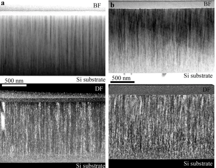
Fig. 2. (a) Bright (BF) and dark (DF) field images of the Ar +12% air sample. (b) Bright (BF) and dark (DF) field images of the Ar +20% air sample.
3.3.1. Films grown with 12% and 20% air in the sputtering gas
Fig. 2 shows the cross section structure of the films. They appear to be composed of a bottom layer, about 200 nm thick, partially amor- phous structure with very slight traces of crystallinity.
Columnar fibers of about 50–100 nm of diameter form above this bottom layer. The dark field images (Fig. 2, bottom) of the films (made using the 200 reflection (see in Fig. 3) for image formation) show that the fibers, though having a single crystalline nature, are very defective and appear to be composed of very small crystallites/cells of slightly different orientation. Stated differently, each fiber is a crystal, frag- mented into cells being highly oriented into a single crystal like struc- ture. This structure will be named as a fragmented grain/crystal structure, each fiber having an individual and close preferred orienta- tion of its cells. This seems, to the best of our knowledge, a new kind of structure observed in MPEA films grown under these conditions. The details of this structure will be discussed further in the text.
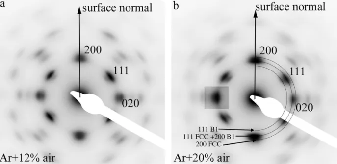
The analysis of the two selected area diffraction patterns (taken over the full film thickness) (Fig. 3) reveals that both films have a strong
〈100〉preferred orientation with rather broad reflections in both radial and azimuthal directions. The broadening of the peaks is due to varia- tions in the lattice parameter, size and orientation of the coherently scattering domains. They also reveal that, in fact, two fcc phases, aligned epitaxially to each other are present in both films. The lattice parameter of the first phase is 0.370 ±0.01 nm, while the other phase has a lattice parameter equal to 0.420 ±0.01 nm. The presence of the two phases agrees with the XRD analysis, although there is some difference with the obtained values for the lattice parameters. As discussed before, this lattice parameter is slightly different from the pure CoCrFeMnNi [21]
due to the incorporation of O and/or N. The latter phase can be attrib- uted to a CoCrFeMnNi-oxynitride in accordance with the X-ray mea- surements (Fig. 1b). The curiosity of these phases is that d(111) of the doped metallic phase (~0.21 nm) practically is equal to the d(200) spacing of the oxynitride phase.
The phase composition of the film, grown in Ar +20% air sputtering gas (Fig. 2b) is very similar to the film grown using Ar + 12% air (Fig. 2a). The only difference is, that SAED reflections belonging to the oxynitride phase are more intense (Fig. 3b), which means an increased fraction of oxynitride in this film, as also observed in the X-ray diffrac- tion analysis (Fig. 1a). We can also note, that the (020) reflection of the
fcc phase is very weak in Fig. 3b. This must be due to low number of fcc [001] orientations perpendicular to the sample plane in the selected area.
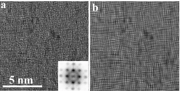
The structure of the 12% and 20% air samples does not show crucial differences on the 10 nm scale and above (Figs. 2 and 3). Therefore, a more detailed structural analysis by HREM measurements on both samples was made. The partially amorphous structure of the bottom layer in the 12% air sample is confirmed also by HREM (Fig. 4). Crys- talline arrangements as small as 1–3 nm can be found in this region, their number and size is increasing with the distance from the substrate.
Moreover, a 〈100〉preferred orientation of the CoCrFeMnNi metallic phase can be traced in the Fast Fourier Transform (FFT) of the HREM image in the very bottom of the film, and its appearance is stronger as measured further from the substrate (Fig. 4b-d).
A high resolution image of a column from the top region of the film (12% air) shows the aforementioned fragmented (mosaic) structure of the fiber (CoCrFeMnNi metallic phase, Fig. 5a). In the image the defective lattice can be observed as no straight lattice fringes are present through the fiber. As a result of the fragmented structure, the diffraction maxima broadened in all directions. The FFT in Fig. 5a shows single crystal pattern of [001] orientation as part of the 〈100〉 preferred orientation. It shows the same broad reflections as observed in the selected area diffraction patterns (Fig. 3). It also indicates the alignment of the two phases in the structure (doubled reflections). The FFT filtered image, generated using only the diffraction maxima of the FFT pattern (in Fig. 5a), highlights the fragmented structure of the film. No notice- able oxynitride nanocrystals are seen, but a variation of the spacing of the lattice fringes is clearly observable (as it follows from the electron diffraction patterns in Fig. 3).
As we can see in Fig. 2, the transition from the partially amorphous bottom layer to the fragmented crystals is rather abrupt. The structure above the transition region changes little, the growth of fragmented, columnar crystals takes place with a slight increase of the column diameter with film thickness.
3.3.2. Structure of films grown with 30% and 50% air in the sputtering gas A comparison of the two structures (Fig. 6) shows that both films have a bottom layer with a thickness of approximately 200 nm, con- sisting of small grains. This layer continues in a columnar structure with
Fig. 3. (a) Selected area electron diffraction (SAED) of film prepared in Ar +12% air. The strong reflections belong to the metallic CoCrFeMnNi phase, the weaker, inner reflections to the CoCrFeMnNi-oxynitride. (b) SAED of film prepared in Ar +20% air. Reflections of the MPEA fcc and the oxynitride B1 phases are indicated.
The intensity of the 0–20 reflection is increased to show its doubled nature.
Fig. 4.HREM image of the partially amorphous structure at the bottom of the film grown in Ar +12% air atmosphere (a) and its fast Fourier transform patterns: b) 10 ×10 nm area, 25 nm above bottom, c) 10 ×10 nm area, 10 nm above bottom and d) 10 ×10 nm area, very bottom. The 〈100〉preferred orientation improves with increasing the distance from the substrate.
Fig. 5. HREM image of the top of the 12% air layer with the FFT pattern of the area (a), and the filtered image of the same area, corresponding to the 200 type diffraction maxima (b).
increasing column diameter towards the surface. The comparison re- veals also two important differences. First, in contrast to the TEM image of the 30% air sample (Fig. 6a), the TEM image of 50 % air sample (Fig. 6c) shows a blurred contrast which indicates a fragmented struc- ture, showing some similarity to the TEM image of the previously dis- cussed 20% sample (Fig. 2b). The fragmented structure is shown in more detail in Appendix A3. The second difference is related to the film sur- face. The 30% sample is rather smooth, while the 50% sample has a wavy surface due the presence of grain boundary grooves. The diffrac- tion patterns in Fig. 6b and d reveal the phases and the preferred orientation in these films. The structure in both films is dominated by a phase having an fcc symmetry and a lattice parameter around 0.42 nm as described in [16], which denotes an CoCrFeMnNi-oxynitride phase with a B1 structure, also observed in the XRD analysis in Fig. 1. The diffraction maxima of the basic B1 phase of the 50% air film are much broader than those of the 30% sample as also observed in the XRD patterns (Fig. 1). In addition, both the 30% and 50% air films have a strong 〈100〉preferred orientation.
The diffraction pattern of both films contains diffuse scattering in- tensity besides the Bragg reflections of the B1 crystalline phase (Fig. 6b
and d). A more intense diffuse scattering is observed in the 50% sample as compared to the 30% sample. This diffuse scattering which falls inside the B1 200 reflection approaches the scattering from a crystalline structure (Fig. 6d) corresponding to a lattice spacing of 0.265 nm.
HREM images near the very bottom of the 30% air film show CoCrFeMnNi–oxynitride crystalline grains with random orientation (Fig. 7). The size of the grains is between 5 and 10 nm, some of them are elongated in the growth direction. They turn into narrow column like crystals in the first 200 nm of the film from where the V-shape columns start to develop.
The single crystal structure of a column for this 30% air sample is shown in Fig. 8. The orientation of this columnar grain corresponds to the 〈100〉preferred orientation of the film, the [200] reciprocal vector being perpendicular to the film surface. The grain is viewed along the [011] zone axis. Compared to Fig. 5 (12% air sample) the lattice fringes are more regular denoting a less fragmented structure and/or larger size of fragments. The FFT, however, shows also a diffuse scattering in the form of long streaks running along the 〈111〉type reciprocal vectors, indicating planar disorder on the {111} planes in the single-crystalline columns (Fig. 8b). For comparison and further discussion, a SAED
Fig. 6. TEM images and diffraction patterns obtained from the whole thickness of the film including also part of Si substrate. The dots in the diffraction patterns belong to Si substrate, they are included for calibration. Figure (a) and (b) are related to the sample deposited in 30% air, while figure (c) and (d) hold the same information for the sample deposited in 50% air.
pattern from a SiO2 polymorph is shown in Fig. A4 (Appendix). The nature of the diffuse scattering is very similar in the two patterns (Figs. 8b and A4 (Appendix)). The diffuse pattern is caused by structural disorder that can be described by the RUM model [22], mentioned also in the introduction.
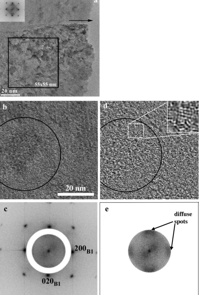
To separate and visualize the structure components that belong to
the diffuse and Bragg scattering, an additional analysis was performed on a single crystalline column (Fig. 9). Again the orientation of the columnar grain corresponds to the 〈100〉preferred orientation of the film, the [200] reciprocal vector is parallel to the surface normal, but the grain, in contrast to Fig. 8, is viewed along the [001] zone axis.
The FFT pattern shown in the insert of Fig. 9a was taken from the 55
×55 nm box, marked in the same figure. Then filtered images were created according to the filter masks shown in Fig. 9c and e. In this way, complementary images were produced, one with the diffuse scattering intensity basically present inside the mask (Fig. 9e) and another image with the remaining scattering, mainly containing the Bragg reflections (Fig. 9c). The two images (Fig. 9b and d) are complementary in the sense of FFT filtering. One shows the ordered (crystalline) fraction without the contribution of the diffuse scattering located inside the white ring (Fig. 9b). This is the B1 oxynitride phase having a regular crystalline lattice (a ≈0.42 nm). The other (Fig. 9d) is showing the fraction of the structure arising from the diffuse scattering corresponding to the spacing of ~0.265 nm and falling in the aperture shown in Fig. 9e. This reveals tiny, distorted crystal-like formations of about a few periods in size as shown in the enlarged insert of Fig. 9d. Besides the diffuse spots, lines of diffuse scattering are present, similar to those observed in Fig. 8, here directed in 〈110〉crystallographic directions of the B1 phase.
A high resolution image of the 50% sample is shown in Fig. 10. The regular lattice seen in the image corresponds to the 0.42 nm lattice parameter, B1 structure (oxynitride). It is also observed that these lattice fringes are not continuous. The continuity and contrast of 200 type fringes changes on about 10 nm scale. This is due to the fragmented structure of the crystal and the slight orientation difference between the fragments (Fig. A5 (Appendix)). The FFT pattern shows also the 110 type reflections which are forbidden in the basic a =0.42 nm B1 structure, proving that ordering on a sublattice of the B1 structure took place. The regions that underwent ordering, and gave rise to 110 type maxima in the FFT pattern, are distributed evenly as can be seen in the filtered image using only the 110 reflections (Fig. A6a (Appendix)). The size of these ordered domains is on the ~2–3 nm scale. A strong diffuse Fig. 7. HREM image and FFT pattern of the bottom 40 nm (square) area of the
30% air film. In the bottom of the image the Si substrate and the native oxide layer on its surface is visible.
Fig. 8. The structure of a column (a) and FFT diffraction pattern (b) of the 30% film about 300 nm above the substrate. The column is single crystalline, the FFT shows strong diffuse scattering. For interpretation see also Fig. A4 (Appendix).
Fig. 9.HREM 〈100〉view, near the top of the 30% air sample (a). FFT filtered images (b and d) from the area marked by the square in panel a. The two FFT patterns (c and e) show the filtering masks applied to generate the images b) and d), respectively. The arrow in (a) marks the growth direction.
scattering and some broad reflections (corresponding again to ~0.265 nm spacing, see also Fig. 9e) are also visible in the FFT pattern (Fig. 10).
Fourier filtering excluding all Bragg reflections has shown that the corresponding fringes, similar to those shown in Fig. 9d, are present in practically the whole area of Fig. 10 (Fig. A6b (Appendix)).
In summary, according to both the diffraction and chemical analysis, the 30% and 50% films are CoCrFeMnNi-oxynitride films with about 0.42 ±0.01 nm lattice parameter and B1 type unit cell. The oxygen content of the films is about 40–45 at. % according to EDS and WDS and can be more than 50 at. % according to XPS, the metal content is 40–50 at. % and about less than 5 at. % nitrogen is also incorporated (Table 1).
The measured metal to (oxygen+nitrogen) ratio supports the formation of the B1 (NaCl)-type unit cell. According to the existence of the diffuse scattering (showing certain alignment with the main CoCrFeMnNi- oxynitride), a disorder is coexisting in the main crystalline phase of the film mainly located to {111} and {110} planes. A second phase seems to be present which can be described as a structure with very diffuse reflections and a lattice spacing corresponding to ~0.265 nm, detected both in SAED (Fig. 6) and FFT patterns (Figs. 8, 9 and 10) of the 30% and 50% air films.
4. Discussion
4.1. Film morphology and growth modes
Our analysis based on X-ray diffraction, EDS as well as electron diffraction and TEM-HREM, provides detailed information on the structural and compositional features of the (CoCrFeMnNi) MPEA films grown by DC magnetron sputtering in Ar +air mixtures. This infor- mation will be used to draw the inference on the growth processes and evolution mechanism of the observed structures.
From Fig. 2 we observe that at low air fractions (12 and 20%), emerging from a thin bottom sublayer, a fragmented columnar structure of the CoCrFeMnNi metallic phase develops. At first sight, this might suggest a zone T structure which is characterized by a random nucle- ation, and an evolutionary overgrowth resulting a thin film with a fiber texture [23]. However, the HREM and FFT analysis are in conflict with this microstructure assignment. Indeed, no random nucleation took
place, but rather an amorphous-nanocrystalline composite is formed in which the crystallites have a 〈100〉preferred orientation already from the very beginning of the growth. This preferential orientation enhances with increasing thickness as can be observed in Fig. 4. As there is no competing growth between different orientations, we cannot attribute the growth mode of the 12% and 20% air samples to zone T. Rather there is a competition in growth between the 〈100〉oriented crystallites and an amorphous structure from which the crystalline phase comes out as the winning one and develops the fiber like columnar 〈100〉textured part of the film. The formation of the nanocomposite together with the forma- tion of the 〈100〉preferred orientation in the bottom ≈200 nm thickness of the 12% and 20% air films is not fully understood yet, but at least a few considerations can be made. The first possibility is a change in the growth temperature. Although the films are deposited at room temper- ature, it is possible that due to the energy flux, the sample temperature slightly increases. Energy flux probe measurements indicate that the temperature doesn't increase more than 100 ◦C, but nevertheless this increase could contribute to the observed growth change. A second possible explanation may be that the impurity content changes as a function of the deposition time. To avoid this possibility, however, the sample was introduced in the vacuum system after a sufficient long target pre-sputtering step. Finally, also the O or N incorporation can provide the driving force giving an enhanced chance to the growth of
〈100〉oriented nuclei [24].
A different behavior is observed for the depositions performed at higher air fractions. The FFT patterns based on the HREM images made close to the sample/substrate interface (Fig. 7) reveal that the film growth for the samples deposited at 30% and 50% air starts by random nucleation. The grains have a V shape single crystalline nature and a competing growth, resulting in a final 〈100〉 preferred orientation (Fig. 6). Hence it can be concluded that the films grown at higher air fractions have a microstructure characteristic for zone T [23]. In the 30% and 50% air CoCrFeMnNi-oxynitride films the 〈100〉 preferred orientation is probably also due to the incorporation of excess oxygen or nitrogen during competing crystal growth [6,8,24].
For all studied films, the fiber like columnar or V shaped crystals observed in the upper part of the film are fragmented (Figs. 2 and 6).
This fragmentation is strong in the 12% and 20% air films, is less present in the 30% air film, but is again strong in the 50% air film. The broad- ening of diffraction peaks in both X-ray and electron diffraction (Figs. 1, 3 and 6) can be connected to the fragmentation of crystals. The electron diffraction maxima are very broad, being extended both in azimuthal and radial directions from their ideal locations. Broadening can origi- nate from changes in the orientation of the crystallites, compositional fluctuations as well as micro strain or the size of the fragments. All these mechanisms can lay at the origin of a stochastic [12], fragmented structure of the crystals (Fig. 2 and Fig. 6).
The TEM analysis also reveals that the surface of the 30% sample is smooth, while the surface of the 50% sample is wavy (Fig. 6) due to grain boundary grooving. This suggests that in the 50% film the excess material, not incorporated into the growing lattice but segregated to the growth surface, is accumulated at the grain boundaries, hindering the grain growth and leading to grooving [23]. These slight structural dif- ferences as well as the lesser fragmentation suggest that the 30% air film is in a state, closest to a (MeOxN1-x type) stoichiometric CoCrFeMnNi- oxynitride composition and a single phase structure as well.
The above analysis allows a better understanding of the observed changes in the XRD patterns (Fig. 1). The 200 maxima in the XRD dif- fractograms (Fig. 1) shift to smaller angles as the fraction of air in sputtering gas increases, which agrees with a slight increase of the lattice parameter. This is in good agreement with the SAED results. Moreover, broadening of the XRD double peaks takes also place with increasing the air content from 12% air to 20% in the sputtering gas. However, peak width for the 30% air sample becomes narrower, and increases again at higher air fractions. This behavior is also connected to the formation of the fragmented structure and the size of the cells/fragments, composing Fig. 10.HREM image of a columnar grain in the 50% air sample and its
FFT pattern.
the crystals of the films.
The intensity of the XRD 200 peaks decreases with increasing the air fraction. One possible explanation can be taken from the paper of Yeh and co-workers [25]. It states that a substantial decrease of the peak intensity can originate from the increasing number of components when they have different atomic size and cause lattice strain. The effect works similar to the Debye-Waller factor and becomes already substantial when a component, having different atomic size from the other two is present on 1/3 of the lattice positions. This condition can become satisfied above 20% of air in sputtering gas. This is in good agreement with compositional measurements (Table 1). However, another effect not mentioned in the work by Yeh, can also contribute. Namely, the atomic scattering factors for low atomic number elements such as oxy- gen and nitrogen are smaller as compared to those for the metal atoms and the scattering amplitude/unit volume decreases. Consequently, as long as metals are present in high concentration, and in our case the metallic atoms are very close in size, we have high intensity (up to 20%
air in the sputtering gas). However, when the oxygen and nitrogen species occupy ≈50% of the atomic sites in the lattice, the intensity drops due to both factors: the increased number of components (and consequently strain) according to [25] and the decrease of the average scattering intensity/unit volume.
4.2. Phases and their nanostructure
As we have seen from the SAED and XRD analysis, the phase composition of the films changes between 20% and 30% air in the sputtering gas. Up to 20% air we obtain metallic (solid solution with O and N) crystals/grains into which a minority oxynitride phase is inter- locked resulting in the fragmented grain structure (Fig. 5). The increase in lattice parameter (Fig. 1) of the metallic phase when changing the air fraction from 12 to 20% can be due to the solute effect (Vegard's law).
Above 30% air the dominating phase is a B1 type oxynitride with a lattice parameter of 0.42 nm.
Besides the main phases and corresponding broad diffraction peaks belonging to crystalline structure identified in Section 4.1 (Figs. 2 and 6), there is strong diffuse scattering visible both in electron diffraction patterns (Figs. 3 and 6) and in FFT patterns (Figs. 8, 9 and 10). In films prepared at 12 and 20% air in sputtering gas a second phase, namely the B1 oxynitride phase could be attributed to the diffuse peaks. In films of 30 and 50% air in sputtering gas the observed diffuse scattering also shows reflection-like features. These features together with the corre- sponding HREM images (Fig. 9d) suggest that a fraction of the film does not belong to the 0.42 nm lattice parameter B1 phase. This fraction must be a kind of complex oxides e.g. similar to Mn-O type systems [26] or perovskites [27]. However, the available diffraction information is insufficient for the phase identification. Fluctuations in the structure of the oxynitride phase are evidenced also by appearing the forbidden 110 reflections in the FFT pattern of the 50% air sample (Fig. 10), which are due to ordering process in the B1 lattice during growth.
As we have seen, the broad reflections of the B1 phase and the diffuse scattering is due to disorder in the crystalline structure. It is quite evident, that different kinds of disorder must be present. These can be fluctuations in the composition, structure, or when the formation energy of metastable or stable phases is very similar, minor fluctuations of phases and/or symmetry can form as well. Also, when different sub- structures coexist in an interlocking structure, fluctuations of strain can be present (Figs. 4, 9 and 10). These characteristics, each alone and several or all together present in a structure on the nanoscale, result in the aforementioned stochastic structures [12]. We suggest that the columnar grains in the films, presented in this paper, have a stochastic structure in which the above fluctuations are present, giving rise to peak broadening and to the diffuse scattering observed in SAED and FFT patterns (Figs. 2, 3, 6, and 8 to 10). The stochastic nature of the structure can also be tracked in the XRD patterns (Fig. 1) in the form of very broad reflections. We consider this kind of structure to be stochastic in the
sense of atomic arrangement and being characteristic for all four films and already partly observed in [6,8].
However, not all kind of diffuse scattering can be attributed to the atomic disorder as discussed above. In addition to the stochastic lattice an ordering-disordering phenomenon can also occur at the level of metal (O,N) octahedra as well. Indeed, as shown in Fig. 8, there is a strong similarity between the observed diffraction pattern (Fig. 8b), and the diffraction pattern (Fig. A4 (Appendix)) of a SiO2 polymorph. As dis- cussed by Dove et al. [22], the formation of the linear intensity distri- bution, connecting the Bragg reflections of a SiO2 crystal can be explained by the collective displacement of SiO4 tetrahedra, described by the Rigid Unit Mode (RUM) model [13]. The similarity of these in- tensity distributions in Fig. 8b, 9 and 10 is very convincing when compared to the one in Fig. A4 (Appendix). The straight diffuse lines connecting the broad reflections in Figs. 8b and 10 must/may arise from a similar effect produced by the metal(O,N)6 octahedra of the oxynitride phase [28]. The RUM model differs in two aspects from the stochastic structures, though the two are compatible with each other. In the RUM model the structural deviations from the average occur by the displacement of rigid structural units composed from several atoms, i.e.
octahedra. These displacements or rotations are not random, rather are arranged on certain crystallographic planes [13]. As a result, perpen- dicular to these planes long streaks will appear in the reciprocal lattice and in the diffraction pattern (Fig. 11). We suggest that they are observed between diffraction peaks in Figs. 8b and 10 but also in Fig. 9 and are of the same origin as the streaks seen in Fig. A4 (Appendix). The streaks are directed along the 〈111*〉type reciprocal lattice directions in Figs. 8b and 10 and along the 〈110*〉in Fig. 9, both directions corre- spond peculiar planes in the B1 (NaCl) type lattice.
Up to now we were able to understand, or at least model the observed structures and diffraction patterns of the CoCrFeMnNi-oxynitride or CoCrFeMnNi metal films with O and N solutes. However, why and how the structural variations happen to form in these stochastic and RUM disordered structures? An answer can be attempted following the results of interpretation of structural peculiarities of Cu-Ag films, grown also by sputtering [14]. In the Cu-Ag films the interlocking Ag/Cu phase- separating structure is supposed to form by spinodal decomposition. In this case we can suggest the same model. During growth of the film, we can imagine that an ideally random structure is deposited, which is, however, unstable. Moreover, this unstable structure can have a number of practically equally probable structural variants, having lower energy than the as formed one. So, still during growth, below the growth surface or surface layer of the “ideally” random structure, spinodal decompo- sition can occur which results in the observed stochastic structure and its RUM variations. Then the structures of slightly different lattices/phases are epitaxially interlocked into the dominant structure. As observed in HREM (Figs. 5 and 9) the result is a spinodally decomposed fragmented stochastic structure, composed of the most easily attainable structures.
The structure is essentially metastable or even still unstable, and only the kinetic possibilities will determine where it stops from further developing. At the present stage of knowledge, we think that the above described structures represent a state which can be reached during the given deposition conditions.
The fragmented and stochastic structure of CoCrFeMnNi-oxynitride films will manifest itself in physical properties as well. For example, regarding mechanical properties, strength and plastic deformation mechanisms depend on structural features, which are considered con- stant on the scale of the slipping segments of a dislocation and/or on the energy of the developing deformation faults/twins/antiphase bound- aries. These structural features are definitely varying in the fragmented and stochastic structure, described in this work. Nanoscale changes of local chemical order/composition or bonding type will strongly influ- ence all deformation mechanisms. The structural heterogeneities on the nanoscale in this case include changing from covalent type oxynitride to metallic alloy, and can present obstacles to dislocation movement thus enhancing the strength of materials, compared to a homogeneous solid
solution. Computer simulation studies [29] have shown that slip pro- cesses in this kind of nanometer scale structures result in increased strength of MPEA materials similarly to the effect of Guinier–Preston zones in alloys. The reported variation of local chemical ordering im- plies nanoscale variation of dislocation pathways and thus deformation mechanisms. So, discovering these kind of structures will promote the understanding/planning of the mechanical parameters of MPEA mate- rials of the same composition but prepared under different experimental conditions.
5. Conclusions
Addition of 4–50% air to Ar in sputtering gas during deposition of CoCrFeMnNi alloy thin films results in a change of the phase state of growing film between Ar +20% and Ar +30% air composition of the sputtering gas.
At 12 and 20% of air a 〈100〉preferred orientation fcc CoCrFeMnNi alloy, doped with oxygen and nitrogen develops, which is stochastically intermixed with a B1 oxynitride nano-phase. The B1 oxynitride nano- phase is embedded epitaxially into the fcc CoCrFeMnNi alloy.
At and above 30% of air a B1 phase 〈100〉preferred orientation CoCrFeMnNi-oxynitride forms. Oxygen is preferentially incorporated into the growing structures, while nitrogen content is inferior. The 〈100〉 preferred orientation is the result of selected nucleation (12 and 20%
air) or competing growth (30 and 50% of air) of the developing crystals.
All films produce broad Bragg peaks and a strong diffuse scattering which can be attributed to the nanoscale stochastic and/or partly or- dered (RUM and ordered fcc) CoCrFeMnNi metal or CoCrFeMnNi- oxynitride lattice. The stochastic and ordered nano-structures are thought to be the result of spinodal processes taking place already during the growth process of the originally homogeneous structure.
These kind of structures and processes can be quite general in MPEA alloys and compounds.
Supplementary data to this article can be found online at https://doi.
org/10.1016/j.surfcoat.2021.127433.
CRediT authorship contribution statement
G. Radnoczi: Conceptualization, Writing- Original, Writing- ´ Reviewing and Editing, Project administration, R. Dedoncker: Meth- odology, Investigation, G.Z. Radnoczi: Investigation, Methodology, Zs. ´ Czig´any: Methodology, Validation, A. Sulyok: Investigation, Formal analysis, V. Kovacs-Kis: Writing- Original, Writing- Reviewing and ´
Editing, Validation, D. Depla: Supervision, Reviewing and Editing, Funding acquisition.
Declaration of competing interest
The authors declare that they have no known competing financial interests or personal relationships that could have appeared to influence the work reported in this paper.
Acknowledgement
This study was supported by the Hungarian National Research Development and Innovation Office through the OTKA NN112156 project. The authors also acknowledge the VEKOP-2.3.3-15-2016-00002 and VEKOP-2.3.2-16-2016-00011 projects of the European Structural and Investment Funds. V. K-K. is indebted to the J´anos Bolyai Fellowship of the Hungarian Academy of Sciences and the ÚNKP-19-4 New National Excellence Program of the Ministry for Innovation and Technology. DD and RDD acknowledge the financial support by the Research Foundation Flanders (project SPADONA G0G6816N).
References
[1] B. Cantor, I.T.H. Chang, P. Knight, A.J.B. Vincent, Microstructural development in equiatomic multicomponent alloys, Mater. Sci. Eng. A 375 (2004) 213–218, https://doi.org/10.1016/j.msea.2003.10.257.
[2] Y. Zhang, T.T. Zuo, Z. Tang, M. Gao, K.A. Dahmen, P.K. Liaw, Z.P. Lu, Microstructures and properties of high entropy alloys, Prog. Mater. Sci. 61 (2014) 1–93, https://doi.org/10.1016/j.pmatsci.2013.10.001.
[3] Gao, M.C. Progress in high-entropy alloys. JOM. 2013, 65, 1749–1750. doi:htt ps://doi.org/10.1007/s11837-013-0788-8.
[4] D.B. Miracle, O.N. Senkova, Acta Mater. 122 (2017) 448–511, https://doi.org/
10.1016/j.actamat.2016.08.081.
[5] Chia-Han Lai, Su-Jien Lin, Jien-Wei Yeh and Andrew Davison Effect of substrate bias on the structure and properties of multi-element (AlCrTaTiZr)N coatings, J. Phys. D. Appl. Phys. 39 (2006) 4628–4633, https://doi.org/10.1088/0022- 3727/39/21/019.
[6] R. Dedoncker, P. Djemia, G. Radn`oczi, F. T´etard, L. Belliard, G. Abadias, N. Martin, D. Depla, Reactive sputter deposition of CoCrCuFeNi in nitrogen/argon mixtures, J. Alloys Compd. 769 (2018) 881–888, https://doi.org/10.1016/j.
jallcom.2018.08.044.
[7] M.-H. Hsieh, M.-H. Tsai, W.-J. Shen, J.-W. Yeh, Structure and properties of two AlCrNbSiTi high-entropy nitride coatings, Surf. Coat. Technol. 221 (2013) 118–123, https://doi.org/10.1016/j.surfcoat.2013.01.036.
[8] R. Dedoncker, G. Radn´oczi, G. Abadias, D. Depla, Reactive sputter deposition of CoCrCuFeNi in oxygen/argon mixtures, Surf. Coat. Technol. 378 (2019), 124362, https://doi.org/10.1016/j.surfcoat.2019.02.045.
[9] Ruei-Sung Yu, Rong-Hsin Huang, Chih-Ming Lee, Fuh-Sheng Shieu, Synthesis and characterization of multi-element oxynitride semiconductor film prepared by Fig. 11.The reciprocal unit cell of the fcc crystal with infinite rods (dotted lines) in 〈111〉directions, due to the planar disorder on {111} planes in the lattice (a) and their geometry in an {110*} reciprocal lattice plane of sample 30% air (b). The dotted lines in a) and b) correspond to linear streaks in the diffraction patterns.
reactive sputtering deposition, Appl. Surf. Sci., Volume 263, 15 December 2012, Pages 58–61 doi:https://doi.org/10.1016/j.apsusc.2012.08.109.
[10] Duc Duy Le, Soon-Ku Hong, Trong Si Ngo, Jeongkuk Lee, Yun Chang Park, Sun Ig Hong, Young-Sang Na, Microstructural investigation of CoCrFeMnNi high entropy alloy oxynitride films prepared by sputtering using an air gas, Met. Mater. Int., November 2018, Volume 24, Issue 6, pp. 1285–1292, doi:https://doi.org/10.100 7/s12540-018-0143-2.
[11] Jeongkuk Lee, Soon-Ku Hong, Structural characterization of CoCrFeMnNi high entropy alloy oxynitride thin film grown by sputtering, Korean J. Mater. Res. 28 (10) (2018), https://doi.org/10.3740/MRSK.2018.28.10.595.
[12] Robert Hull, Pawel Keblinski, Dan Lewis, Antoinette Maniatty, Vincent Meunier, Assad A. Oberai, Catalin R. Picu, Johnson Samuel, Mark S. Shephard,
Minoru Tomozawa, Deepak Vashishth, Shengbai Zhang, Stochasticity in materials structure, properties, and processing—a review, Appl. Phys. Rev. 5 (2018), 011302, https://doi.org/10.1063/1.4998144.
[13] A.P. Giddy, M.T. Dove, G.S. Pawley, The determination of rigid-unit modes as potential soft modes for displacive phase transitions in framework crystal structures, Acta Cryst A49 (1993) 697–703, https://doi.org/10.1107/
S0108767393002545.
[14] F. Misj´ak, P.B. Barna, G. Radn´oczi, Growth of nanocomposite in eutectic Cu–Ag films, Thin Solid Films 518 (2010) 4247–4251, https://doi.org/10.1016/j.
tsf.2009.12.095.
[15] G. Radn´oczi, E. Bok´anyi, Z. Erd´elyi, F. Misj´ak, Size dependent spinodal decomposition in Cu-Ag nanoparticles, Acta Mater. 123 (2017) 82–89, https://doi.
org/10.1016/j.actamat.2016.10.036.
[16] B.R. Braeckman, F. Boydens, H. Hidalgo, P. Dutheil, M. Jullien, A.-L. Thomann, D. Depla, High entropy alloy thin films deposited by magnetron sputtering of powder targets, Thin Solid Films 580 (2015) 71–76, https://doi.org/10.1016/j.
tsf.2015.02.070.
[17] B.R. Braeckman, D. Depla, On the amorphous nature of sputtered thin film alloys, Acta Mater. 109 (2016) 323–329, https://doi.org/10.1016/j.actamat.2016.02.035.
[18] W.P. Leroy Boydens, R. Persoons, D. Depla, Deposition of thin films by sputtering cold isostatically pressed powder targets: a case study, Phys. Status Solidi (a) 209 (3) (2012) 524–530, https://doi.org/10.1002/pssa.201127490.
[19] F. Boydens, W.P. Leroy, R. Persoons, D. Depla, The influence of target surface morphology on the deposition flux during direct-current magnetron sputtering, Thin Solid Films 531 (2013) 32–41, https://doi.org/10.1016/j.tsf.2012.11.097.
[20] B.V. Crist, Handbook of Monochromatic XPS Spectra: Elements and Native Oxides, Wiley, New York, 2000, ISBN 978-0-471-49265-8.
[21] B. Braeckman, P. Djemia, F. T´etard, L. Belliard, D. Depla, Impurity-controlled film growth and elastic properties of CoCrCuFeNi thin films, Surf. Coat. Technol. 315 (2017) 475–483, https://doi.org/10.1016/j.scriptamat.2017.06.046.
[22] M.T. Dove, K.D. Hammonds, V. Heine, R.L. Withers, Y. Xiao, R.J. Kirkpatrick, Rigid unit modes in the high-temperature phase of SiO2 tridymite: calculations and electron diffraction, Phys. Chem. Miner. 23 (1996) 56–62, https://doi.org/
10.1007/BF00202994.
[23] I. Petrov, P.B. Barna, L. Hultman, J.E. Greene, Microstructural evolution during film growth, J. Vac. Sci. Technol. 21 (5) (2003) S117–S128, https://doi.org/
10.1116/1.1601610.
[24] Barna, P.B.; Biro, D.; Hasaneen, M.F.; Sz´ekely, L. Menyh´ard, M.; Sulyok, A.;
Horv´ath, Z.E.; Pekker, P.; D´odony, I.; Radn´oczi, G., Cross sectional complex structure analysis is a key issue of thin film research: a case study on the preferential orientation crossover in TiN thin films, Thin Solid Films 688 (2019) 137478 doi:https://doi.org/10.1016/j.tsf.2019.137478.
[25] Jien-Wei Yeh, Shou-Yi Changb, Yu-Der Hong, Swe-Kai Chen, Su-Jien Lin, Anomalous decrease in X-ray diffraction intensities of Cu–Ni–Al–Co–Cr–Fe–Si alloy systems with multi-principal elements, Mater. Chem. Phys. 103 (2007) 41–46, https://doi.org/10.1016/j.matchemphys.2007.01.003.
[26] Pacalo R E G, Graham E K, Physics and chemistry of minerals 18 (1991) 69-80, Pressure and Temperature Dependence of the Elastic Properties of Synthetic MnO, Database Code amcsd 0007528], a=0.445, FCC doi:https://doi.org/10.1007/B F00199046.
[27] Sicong Jiang, Tao Hu, Joshua Gild, Naixie Zhou, Jiuyuan Nie, Mingde Qin, Tyler Harrington, Kenneth Vecchio, Jian Luo, A new class of high-entropy perovskite oxides, Scr. Mater. 142 (2018) 116–120.
[28] Ray L. Withers, Disorder, structured diffuse scattering and the transmission electron microscope, Z. Kristallogr. 220 (2005) 1027–1034.
[29] Qing-Jie Li, Howard Sheng, Evan Ma, Strengthening in multi-principal element alloys with local-chemical-order roughened dislocation pathways, Nat. Commun.
10 (2019), 3563, https://doi.org/10.1038/s41467-019-11464-7.