See discussions, stats, and author profiles for this publication at: https://www.researchgate.net/publication/329992517
Effect of different active screen hole sizes on the surface characteristic of plasma nitrided steel
Article in Results in Physics · December 2018
DOI: 10.1016/j.rinp.2018.12.079
CITATIONS
0
READS
43 3 authors:
Some of the authors of this publication are also working on these related projects:
Role of nitrogen in welding of duplex stainless steelsView project
Hungarian MMC researchesView project Dorina Kovács
Budapest University of Technology and Economics 7PUBLICATIONS 3CITATIONS
SEE PROFILE
Janos Dobranszky
Hungarian Academy of Sciences 105PUBLICATIONS 386CITATIONS
SEE PROFILE
Attila Bonyár
Budapest University of Technology and Economics 65PUBLICATIONS 264CITATIONS
SEE PROFILE
All content following this page was uploaded by Attila Bonyár on 12 March 2019.
The user has requested enhancement of the downloaded file.
Contents lists available atScienceDirect
Results in Physics
journal homepage:www.elsevier.com/locate/rinp
Effect of different active screen hole sizes on the surface characteristic of plasma nitrided steel
Dorina Kovács
a,⁎, János Dobránszky
b, Attila Bonyár
caBudapest University of Technology and Economics, Faculty of Mechanical Engineering, Department of Materials Science and Engineering, Műegyetem rkp. 3, 1111 Budapest, Hungary
bMTA–BME Research Group for Composite Science and Technology, Műegyetem rkp. 3, 1111 Budapest, Hungary
cBudapest University of Technology and Economics, Department of Electronics Technology, Egry József Street 18, 1111 Budapest, Hungary
A R T I C L E I N F O Keywords:
Active screen plasma nitriding Hole size
Surface characterisation AFM
A B S T R A C T
Active screen plasma nitriding (ASPN) was performed on tempered 42CrMo4 low alloy steel samples. The effects of two technological parameters, namely 1) the hole size of the screen and 2) the open area ratio were in- vestigated on the properties of the developed nitride layer. Scanning electron microscopy (SEM), atomic force microscopy (AFM) and Vickers microhardness testing were used for the characterization of the surface. The thickness of the nitride layer, the microhardness and the length of the nitride diffusion zone and surface areal parameters like surface roughness, skewness, grain diameter and area were measured and correlated with the screen hole size and open area ratio. It was found that these two major technological parameters influence different aspects of the developed nitride layer. The layer thickness and surface skewness (connected to either a balanced surface with zero skewness or the appearance of hill-like complex structures with positive skewness) is more sensitive to the open area ratio, while the surface roughness is primarily a function of the hole size. The maximum surface hardness, the length of the nitride diffusion zone or the size (diameter and surface area) of the nitride grains did not show a strong correlation with either of these two parameters.
Introduction
Plasma nitriding is a surface treatment widely used in the industry to improve the hardness, the wear and in some cases the corrosion resistance of steels. One type of this technology is the active screen plasma nitriding (ASPN), which is becoming increasingly widespread among the surface hardening techniques. In this case, the sample is electrically isolated from the voltage source and the plasma is formed on the screen placed around the sample[1]. The specimen is heated by radiation and the ASPN generates a nitrogen mass transfer to its surface [2,3].
Previous papers already discussed the pros and cons of ASPN compared to DCPN (direct current plasma nitriding), such as edge and hollow cathode effects, regarding the resulting surface properties[4–6].
The edge effect, which is one of the major shortcomings of DCPN, can be perfectly eliminated with ASPN, preventing the breaking of the corners[7,8]. Besides, the hardness of the nitrided layer is more even with ASPN[9,10]and the layer thickness can also be higher with in- creased temperature[11,12].
During ASPN several technological parameters, such as the material and the geometry of the active screen, the time and temperature in- fluence the resulting properties, especially the layer thickness, hardness and surface roughness of the formed nitride layer. Previous studies aimed to characterize the connection between these parameters, for example the effect of the distance between the sample and the active screen was investigated in several works[13–15]. However, none of the previous works provided a definite answer regarding the effect of the active screen hole sizes on the developed surface properties, although some of them did mention and touch this parameter, to a limited extent.
For example, Sousa et al. nitrided different austenitic stainless steel samples with ∅8 mm hole size in a cage with ∅112 mm diameter. The results showed uniform phases and layer thickness on the surface and a similarly good surface hardness on all samples[16]. The effect of the N2
ratio in the gas mixture was also characterized. The resulting layer thickness and hardness decreased in pure nitrogen atmosphere and the highest values were found to be at 80% N2content[17]. By increasing the gas pressure, the previously mentioned properties also increased [18]. Nishimoto et al. used three types of austenitic stainless steel active
⁎Corresponding author at: Department of Materials Science and Engineering, Faculty of Mechanical Engineering, Budapest University of Technology and Economics, Műegyetem rakpart 3, Budapest 1111, Hungary.
E-mail address:dorina@eik.bme.hu(D. Kovács).
T
screen cages (such as pipe, foil, and wire mesh) and compared the re- sulting properties of the nitride layer with DCPN. They found that the hole size of the cage had a slight influence on the surface properties, namely that the surface of the sample treated with the wire mesh screen were slightly finer than those treated with screens with 5 mm holes [19]. Taherkhani compared the effect of screens with 6 mm and 8 mm holes with various top lids on low alloy steel. He reported that the re- sulting hardness is higher by performing the procedure under screen lid than under plate, because of the greater movement of iron nitride from the top lid holes[20]. However, this research still does not discuss the effect of different screen hole sizes in detail. Naam et al. also used these two types of hole sizes, but within one screen, and analyzed the effect of different diameters on unalloyed steel. He found that while reducing the diameter of the active screen, the distance between the sample and the screen as well as the current density changed, therefore an optimum active screen diameter existed to maximize the ion flux on the speci- men’s surface. This depends on only the diameter of the screen, not the hole size[21].
Not just only few researchers disclose the utilized hole sizes, the open area ratio of their screen is also rarely given or discussed. This parameter gives the percentage of open area under the screen, and is also expected to have an influence on the properties of the plasma treated surface. Hubbard et al. used a cage with 47% open area ratio and different electric arrangements and described the most significant nitrogen transfer mechanisms of ASPN based on the experiments[22].
Nishimoto et al. also studied the open area ratio, the effect of 38%, 48%
and 63% ratios were compared during active screen plasma nitriding.
Compared to the previously used holes with circular cross section, in this case square forms were used on the screen. The thickness of the nitrided layer increased with decreasing open area ratio of the screen. A schematic illustration of the mechanism of nitrogen mass transfer in ASPN process was presented, which explained that at a lower open area ratio, the number of sputtered particles on the active screen increased because of the large area of screen material. Although similar open area ratios could be prepared with larger holes, the effect of hole size was not investigated[23].
Besides these previously mentioned properties, the resulting roughness of the surface is also a non-negligible factor. ASPN modifies the surface roughness due to the sputtering. At DCPN the roughness of the surface was found to increase with the time of nitriding. The ni- triding time increases the size of microstructures, which start to overlap resulting in bigger cones with different morphologies and lower surface
density[24,25].
The aim of this research is to investigate the effect of different active screen hole sizes during plasma nitriding and analyze the resulting surface properties, the thickness and hardness of the nitrided layer.
Furthermore, the influence of the open area ratio and the hole size will be compared.
Material and methods Sample preparation
A tempered 42CrMo4 low alloy steel was used for the experiments with chemical compositions shown inTable 1. The material was cut into disks with 20 mm diameter and 6 mm thickness. The surface of the samples was wet ground with 80–2500 grit SiC and finely polished with a 3 μm diamond suspension, degreased with acetone in an ultrasonic bath and dried with air.
Plasma nitriding
The plasma nitriding experiments were made in a custom laboratory equipment. The active screen used for the plasma nitriding was made from a 1.0330 type unalloyed steel. The dimensions of the screen were
∅100 × 85 × 0.8 mm, with different hole sizes, which are given to- gether with the nitriding parameters inTable 2. As can be seen in the table, concerning the time, temperature, or content and pressure of the gas mixture, all experiments were performed with the same experi- mental conditions. The sample was placed at the center of the active screen, the distance from the top lid was 35 mm. The temperature was monitored by using an isolated K-type thermocouple under the work- piece. The constant temperature of the samples was regulated by the applied voltage, which was proportional to the open area ratio (the percentage of open holes in the active screen), as can be seen inTable 2.
After placing the sample on the holder, the pressure of the chamber was decreased to around 0.16 mbar. First, the chamber was flushed with argon, then the pressure was set to 2.8 mbar with the gas mixture used for the nitriding (75% N2–25% H2). The 4 h treatment time started when the sample reached the 490 °C nitriding temperature. After the process the sample was cooled under the operating pressure and gas to 300 °C, then air was introduced into the chamber and the sample cooled down to room temperature.
Table 1
The chemical composition of the material in wt%.
C Si Mn P S Cr Mo
42CrMo4 0.38–0.45 ≤0.4 0.6–0.9 ≤0.025 ≤0.035 0.9–1.2 1.5–0.3
Table 2
The applied plasma nitriding conditions for the 42CrMo4 samples.
Sample no. Hole size (mm) Open area ratio (%) Voltage (V) Current (I) Temp. (°C) Time (h) Pressure (mbar) Gas mixture
d4.5 ∅4.5 50 430 1 490 4 2.8 75% N2–25% H2
d8 ∅8 61 468 1
d12 ∅12 50 485 0.9
d18 ∅18 74 532 0.9
d25 ∅25 61 540 0.8
d45 ∅45 87 636 0.7
D. Kovács et al. Results in Physics 12 (2019) 1311–1318
1312
Characterization methods
The hardness of the nitrided samples were measured with a Vickers microhardness tester (Buehler IndentaMet 1105, 10 g load), while a Zeiss EVO MA10 scanning electron microscope (SEM) vas used for the cross-sectional investigations.
For surface characterization a Veeco (lately Bruker) diInnova type atomic force microscope (AFM) was used in contact-mode with an ART D160 diamond probe (spring constant: 5 N/m). The images were ob- tained in 2 µm × 2 µm and 10 µm × 10 µm scan sizes, with a sampling resolution of 512 × 512 and 1 Hz scan rate. The obtained images were post-processed with the Gwyddion 2.36 software[26]. Only standard background correction was applied on the images to remove piezo movement and sample tilt effects. Surface roughness (Sa, Sq) and skewness (Ssk) values were calculated based on Eqs.(1)–(3), defined by the ISO 25178-2 (2012) standard, where Nis the number of height points of the image,ηiis the distance between a height point (zi) and the central plane defined for the surface andµnis then-th second central moment of the height distribution. For every sample a number of 8 images per scan size – obtained in different positions on the surface – were used for the mean and standard deviation calculations. The sur- face area of the grains and the equivalent diameter of the projected grains were calculated with the built-in functions of the Gwyddion 2.36 software, after masking the independent grains on the image. The equivalent grain diameter is the diameter of the disc with the same projected area as the grain. The surface area is calculated by a trian- gulation scheme, described in detail in the Gwyddion user guide[26].
S N1
a | |
i N
i 1
=
= (1)
Sq N1 i µ
i N
2 1
21/2
= =
= (2)
N N
µ S µ
1
sk 1
i i
N
i i N
3 1 2 1
3/2 3
23/2
= = =
= (3)
Results and discussion SEM investigations
The microstructure of the nitrided samples and the formed com- pound layers are presented in the SEM images of Fig. 1. The layer thicknesses, which were calculated based on these images are given in Table 3. To increase the contrast and visibility of the features all sam- ples were etched in 2% Nital. The measured layer thicknesses range roughly between 3 and 4 μm, with the largest difference measured between samples d12 and d18. However, by comparing the images and the data inTable 3, it can be seen that the resulting layer thickness is more sensitive to the open area ratio, than to the hole size. The thickest layers were produced with 50% open area ratio (3.6 to 4 μm), while 61% resulted in 3.4–3.5 μm thickness. However, the effect of hole sizes is not entirely clear. In Fig. 1, the images are paired in a way that samples with the same open area ratio are placed together. At 50%
open area ratio the larger hole size resulted in a thicker layer. The same is true for the samples with the highest open area ratio: sample d45 resulted in a thicker layer compared to d18 (open area ratio is 87% and Table 3
Layer thicknesses of the nitrided samples.
Sample no. Open area ratio (%) Layer thickness (μm)
d4.5 50 3.6
d8 61 3.5
d12 50 4.0
d18 74 3.1
d25 61 3.4
d45 87 3.3
74%, respectively). The two samples with 61% open are ratio resulted in nearly the same layer thickness. Based on this, we might say that larger hole sizes result in higher layer thicknesses, but the open area ratio is clearly the more dominant parameter in the process. Also, the two samples prepared with 50% open area ratio have less even nitride layers (Fig. 1top row). This phenomenon confirms the previous re- search, where the thickness of the nitride layer increased with de- creasing open area ratio[23].
Microhardness
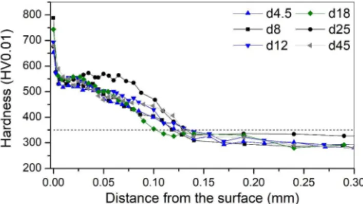
Fig. 2shows the cross-sectional hardness profiles of the nitrided sam- ples. In all cases the average of three measurements is presented. Again, the samples are paired based on their open area ratio. The dashed lines mark the end of the diffusion zone, which is calculated as the base hardness of the sample plus 50HV. The samples are evaluated based on their maximal measured hardness and the length of the diffusion zone inFig. 3.
As it can be seen, all samples show high surface hardness that drops decreasingly until reaching the substrate hardness value. The maximum hardness of the samples were ranging roughly between 650HV0.01 to 800HV0.01, which was measured on the d8 sample. The differences in the lengths of the diffusion zones are within 20 μm. Looking at the data inFig. 3no apparent correlation can be observed between the measured
parameters (maximum hardness and length of the diffusion zone) and the hole size or open area ratio. Samples with the same open area ratio (plotted with the same color inFig. 2) can have similar cross-sectional hardness profiles, e.g. d4.5 and d12 for 50% open area ratio, or sig- nificantly different, e.g. d8 and d25 for 61% open area ratio. For both pairs the samples treated with smaller hole size have shorter diffusion zones. It is interesting to mention that the two samples with the highest maximum hardness (d8, d18) have the shortest diffusion zones.
Surface characterization
Figs. 4 and 5 presents sample contact-mode AFM images in two different scan sizes from the nitrided samples. It can be seen, that the surface has a grainy morphology, which is structured in different levels.
Besides the grains we can observe surface waviness with hills and valleys (e.g.Fig. 4top row for d4.5, d12), and also larger, complex morphologies, which resemble aggregated grains, most visible most visible in the 10 μm × 10 μm images inFig. 5for d8 and d45. This confirms, that the treated surfaces have different characteristic features depending on the applied technological parameters, and since these features have different spatial frequency, the measured surface de- scribing parameters (surface roughness, skewness) are depending on the scan-size, as proved byFig. 6.
Fig. 2.Cross sectional hardness profiles of the nitrided samples.
Fig. 3.Maximum measured hardness and diffusion zone length of the nitrided samples.
D. Kovács et al. Results in Physics 12 (2019) 1311–1318
1314
It is important to note, that the freshly polished reference samples have a surface roughness around 0.75 nm (Sa)/1.3 nm (Sq), which was expected[27,28], so the increase in the roughness is in the 30×–70×
range, depending on the applied hole size. Compared to the overall thickness of the nitride layer (between 3 and 4 μm, Table 3), the 150–250 nm absolute height of the finer microstructure (based on Fig. 4) is less than 10% of the whole layer. However, the 10 µm × 10 µm images ofFig. 4shows, that this absolute height dif- ference can reach 0.6 µm (even around 20% of the layer thickness), caused by the surface waviness and mentioned complex morphologies.
This is also visible on the SEM cross-sectional images ofFig. 1, which are in good accordance with the AFM images (e.g. sample d12 shows
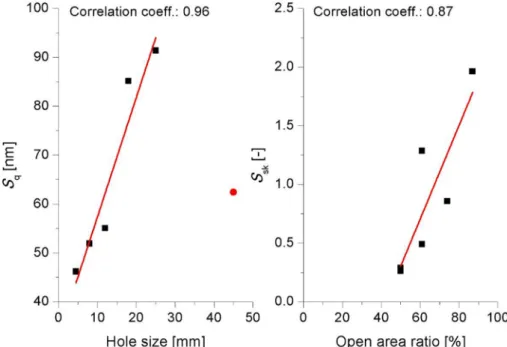
measured with the larger scan size. The surface roughness shows a first slow than after d12 more pronounced increase in function of the hole size, which drops back for the d45 sample. It is interesting to see, that for smaller hole sizes (d4.5, d8, d12) the resulting surface roughness was insensitive to the ratio of open area. The highest sur- face roughness was measured for the second largest diameter of d25, which also has a high, 61% open area ratio. In the case of d45 the significantly higher open area (only 87%) seems to limit the process, thus it resulted in smaller surface roughness compared to d18 or d25.
As presented inFig. 9, considering d45 as an outlier, the correlation coefficient between the surface roughness (for 10 µm × 10 µm images) and the hole diameter is 0.96. Based on the results it is clear, that the Fig. 4.Contact-mode AFM images of nitrided samples. Top row: d4.5, d8, d12; bottom row: d18, d25, d45. Scan size: 2 µm × 2 µm.
Fig. 5.3D contact-mode AFM images of nitrided samples. Top row: d4.5, d8, d12; bottom row: d18, d25, d45. Scan size: 10 µm × 10 µm.
However, due to the simple average based nature of surface roughness, it is possible that surfaces with different characteristics end up having the same roughness value, which can be observed by com- paring the AFM images for the samples having similar roughness, like d4.5, d8, d12. For the sake of deeper understanding, the differences in the surface characteristics, the equivalent grain diameters and grain surface areas were also calculated and given inFig. 7.
It is important to note, that these values were calculated based on the 2 µm × 2 µm images, so they only focus on the grainy
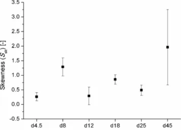
microstructure and exclude the larger, complex morphologies. It is rather interesting to see, that while sample d25, which has the highest surface roughness also has the biggest grains, sample d4.5 has a comparably large grain size, while having the smallest surface roughness. Although the grain sizes presented inFig. 7do not have any apparent correlation with either the hole size or the open area ratio, comparing them, with the skewness values given in Fig. 8 (calculated for the 10 µm × 10 µm AFM images) gives us useful in- formation.
Fig. 6.Surface roughness (Sa,Sq) values measured based on the AFM images with different scan sizes (left: 2 µm × 2 µm; right: 10 µm × 10 µm). For all cases the mean and standard deviation measured on 8 different images are presented.
Fig. 7.Equivalent projected grain diameter and grain surface area values measured based on the 2 µm × 2 µm AFM images for the nitrided samples.
Fig. 8.Skewness (Ssk) values calculated based on the on the 10 µm × 10 µm AFM images for the nitrided samples.
D. Kovács et al. Results in Physics 12 (2019) 1311–1318
1316
The skewness characterizes the symmetry of the height distribution function (HDF) of the surface. In a figurative way a surface with ba- lanced features has a skewness close to zero, a generally flat surface with holes has negative skewness, while we can expect positive skew from a generally flat surface with hills as characteristic features. It can be observed, that the calculated skewness inFig. 9is in negative cor- relation with the grain size: for bigger grains (d4.5, d25, d12) the surfaces have rather balanced features on a large scale (the skewness was calculated for 10 µm × 10 µm areas), while for smaller grains (d8, d18, d45) the skewness is higher, indicating larger hill-like complex morphologies on the surface, also visible inFig. 5. Based on the results it seems, that the appearance of such larger structures and accom- panying smaller grain sizes can be attributed to smaller open area ratios and probably can be connected to more intensive sputtering. The only slight exception in this observation is sample d8, where a relatively larger open area ratio (61%) resulted in smaller grains with some larger features. Considering skewness and the appearance of such complex morphologies, the open area ratio seems to be the governing parameter, as confirmed byFig. 9.
Conclusion
The effects of screen hole size and open area ratio, as two major parameters of active screen plasma nitriding, on the properties of the developed nitride layers were investigated. It was found that the thickness of the nitride layer is primarily a function of the open area ratio. The microscopic surface roughness was found to increase with the hole size of the screen, however increasing the open area ratio was found to increase the skewness, resulting in a less balanced surface with complex morphologies. The cross-sectional microhardness profiles were not correlating strongly with any of the technological parameters.
Conclusively, it was demonstrated that the screen hole size and open area ratio influence different aspects of the developed nitride layer and they should be set in accordance with the needs of the user or specific application.
paper was partially supported by the Higher Education Excellence Program of the Ministry of Human Capacities in the frame of Nanotechnology and Materials Science research area of Budapest University of Technology and Economics (BME FIKP-NAT). It also supported by the ÚNKP-18-3 New National Excellence Program of the Ministry of Humans Capacities.
References
[1] Andrea SB, Mária KB, Mária MB. Nitridálás – korszerű eljárások és vizsgálati módszerek [Nitriding – modern technincs and measurements] Miskolc. Miskolc:
Miskolci Egyetem; 2012. (in Hungarian).
[2] Li CX, Bell T. Corrosion properties of active screen plasma nitrided 316 austenitic stainless steel. Corros Sci 2004;46:1527–47.
[3] Li CX, Georges J, Li XY. Active screen plasma nitriding of austenitic stainless steel.
Surf Eng 2002;18:453–7.
[4] Li Y, Wang L, Shen L, Zhang D, Wang C. Plasma nitriding of 42CrMo low alloy steels at anodic or cathodic potentials. Surf Coat Technol 2010;204:2337–42.
[5] Li CX. Active screen plasma nitriding – an overview. Surf Eng 2010;26:135–41.
[6] Burlacov I, Spies H, Biermann H, Köhler S, Le Thien H. Investigation on the active screen plasma nitriding. Nitriding and Nitrocarburising. 2010. p. 29–30.
[7] Alves C, de Araújo FO, Ribeiro KJB, da Costa JAP, Sousa RRM, de Sousa RS. Use of cathodic cage in plasma nitriding. Surf Coat Technol 2006;201:2450–4.
[8] Corujeira Gallo S, Dong H. On the fundamental mechanisms of active screen plasma nitriding. Vacuum 2009;84:321–5.
[9] Han L, Dai JT, Huang XR, Zhao C. Study on the fast nitriding process of active screen plasma nitriding. Phys Procedia 2013;50:94–102.
[10] Zhao C, Li CX, Dong H, Bell T. Study on the active screen plasma nitriding and its nitriding mechanism. Surf Coat Technol 2006;201:2320–5.
[11] Naeem M, Zaka-ul-islam M, Sha M, Bashir MI, Díaz-guillén JC, Zakaullah M.
Influence of cathodic cage diameter on mechanical properties of plasma nitrided AISI 304 steel. Surf Coat Technol 2017;309:738–48.
[12] Ahangarani S, Mahboubi F, Sabour AR. Effects of various nitriding parameters on active screen plasma nitriding behavior of a low-alloy steel. Vacuum
2006;80:1032–7.
[13] Nishimoto A, Nagatsuka K, Narita R, Nii H, Akamatsu K, Canale L, et al. Effect of gas pressure on active screen plasma nitriding response. J ASTM Int 2011;8:103286.
[14] Naeem M, Shafiq M, Zaka-ul-Islam M, Nawaz N, Díaz-Guillén JC, Zakaullah M.
Effect of cathodic cage size on plasma nitriding of AISI 304 steel. Mater Lett 2016;181:78–81.
[15] Nishimoto A, Nagatsuka K, Narita R, Nii H, Akamatsu K. Effect of the distance between screen and sample on active screen plasma nitriding properties. Surf Coat Technol 2010;205:8–11.
Fig. 9.Correlations between left: the surface roughness (measured on 10 µm × 10 µm AFM images) and the hole size, with d45 considered outlier for fitting and coefficient calculation, right: the skewness and the open area ratio.
[18] de Sousa RRM, de Araújo FO, da Costa JAP, Dumelow T, de Oliveira RS, Alves C.
Nitriding in cathodic cage of stainless steel AISI 316: influence of sample position.
Vacuum 2009;83:1402–5.
[19] Nishimoto A, Tokuda A, Akamatsu K. Effect of through cage on active screen plasma nitriding properties. Mater Trans 2009;50:1169–73.
[20] Taherkhani F, Taherkhani A. Surface characterization of through cage plasma ni- triding on the surface properties of low alloy steel. Sci Iran Sharif Univ Technol 2010;17(4):253–63.
[21] Naeem M, Sha M, Zaka-ul-islam M, Ashiq A, Díaz-guillén JC, Shahzad M, et al.
Enhanced surface properties of plain carbon steel using plasma nitriding with austenitic steel cathodic cage. Mater Des 2016;108:745–53.
[22] Hubbard P, Dowey SJ, Partridge JG, Doyle ED, McCulloch DG. Investigation of nitrogen mass transfer within an industrial plasma nitriding system II: application of a biased screen. Surf Coat Technol 2010;204:1151–7.
[23] Nishimoto A, Matsukawa T, Nii H. Effect of screen open area on active screen plasma nitriding of austenitic stainless steel. ISIJ Int 2014;54:916–9.
[24] Wang Q, Zhang L, Shen H. Microstructure analysis of plasma nitrided cast/forged CoCrMo alloys. Surf Coat Technol 2010;205:2654–60.
[25] Corengia P, Ybarra G, Moina C, Cabo A, Broitman E. Microstructural and topo- graphical studies of DC-pulsed plasma nitrided AISI 4140 low-alloy steel. Surf Coat Technol 2005;200:2391–7.
[26] Nečas D, Klapetek P. Gwyddion: an open-source software for SPM data analysis. J Phys 2012;10:181–8.
[27] Wang Q, Huang C, Zhang L. Microstructure and tribological properties of plasma nitriding cast CoCrMo alloy. J Mater Sci Technol 2012;28:60–6.
[28] Li Y, He Y, Xiu JJ, Wang W, Zhu YJ, Hu B. Wear and corrosion properties of AISI 420 martensitic stainless steel treated by active screen plasma nitriding. Surf Coat Technol 2017;329:184–92.
D. Kovács et al. Results in Physics 12 (2019) 1311–1318
1318
View publication stats View publication stats