Simulation of MNOS memory hysteresis - Effect of layer thicknesses
K. Z. Molnár 1,2, and Zs. J. Horváth 2,3
1 Óbuda University, Doctoral School of Applied Informatics, Budapest, Bécsi út 96/B, H-1084 Hungary
2 Óbuda University, Kandó Kálmán Faculty of Electrical Engineering,
Institute of Microelectronics and Technology, Budapest, Tavaszmező u. 15-17, H-1084 Hungary
3 Hungarian Academy of Sciences, Research Centre for Natural Sciences,
Institute for Technical Physics and Materials Science, Budapest, P. O. Box 49, H-1525 Hungary molnar.karoly@kvk.uni-obuda.hu
horvzsj@mfa.kfki.hu
Abstract— MNOS memory hysteresis curves are simulated by integrating the difference of the current via the oxide and nitride layer. The effect of the oxide and nitride thickness as well as the depth of charge centeroid is studied. The results indicate that the optimal oxide thickness is about 2 nm. A thin nitride layer decreases the efficiency of the injected charge. It has been obtained that the possible highest memory window width decreases monotonically with increasing depth of charge centroid.
I. INTRODUCTION
The two basic types of memory elements used in non- volatile (EEPROM and flash) memories are the floating gate and the SONOS (silicon-oxide-nitride-oxide-silicon) field effect transistors (FETs). Floating gate memory arrays face difficulties with technology scale-down. The main problem is that through defects or weak points of tunnel oxide with reduced thickness the whole amount of stored charge carrying the information can be lost. One of the possible solutions is to replace floating gate with separated semiconductor nanocrystals, which are electrically isolated [1-10].
But, in SONOS and MNOS (metal-nitride-oxide- silicon) devices (the latter were the first realized memory structures [11]) the charge is stored in traps located in the Si3N4 layer close to the Si3N4/SiO2 interface. In these structures traps are isolated a'priori [8-10]. Therefore, these structures are more scalable without using nanocrystals. However, as the reduction of lateral dimensions involves the reduction of layer thicknesses as well, the study of their effect on the memory behaviour is important and topical.
One of the characteristic features of MNOS memory structures is the hysteresis of the threshold voltage of field effect transistors or of the flat-band voltage of capacitors on the amplitude of charging voltage pulses [11-15]. In this work memory hysteresis curves obtained by computer simulation are presented. The effect of the layer thicknesses, namely of the oxide and nitride thickness and of the depth of the injected charge centroid on the hysteresis behaviour have been studied.
is the reduction of current level via the control layer by an additional oxide layer on the top of the structure.
II. SIMULATION DETAILS
The charge injected via the thin oxide layer is captured and stored in traps in the nitride layer close to the oxide/nitride interface. The net charge captured in the nitride layer during a voltage pulse can be calculated by the integration of the difference of the current flowing into the structure via the oxide layer and that of flowing out of structure via the nitride layer, over the charging pulse width τ [11]:
( )
∫
−= Δ
σ
τ0
3 Jox Jn dt (1)
The oxide current can be expressed as [12]:
P E C
Jox = FN ox2 (2)
where CFN is a constant, Eox the electric field in the oxide and P the tunneling probability via the potential barrier, which can be expressed as [16]:
⎟⎟
⎟
⎠
⎞
⎜⎜
⎜
⎝
⎛
−
−
=
∫
21
*[ ( ) ]
2 2 exp
x x
dx E x U m
P = (3)
Here x1 and x2 are the coordinates, where the electron enters and leaves the potential barrier (turning points), m*
is the effective mass of the electron, ħ is the Planck constant (devided by 2π), U(x) is the potential energy as a function of coordinate, and E is the electron energy.
The current via the nitride layer has been obtained by experiment [17]:
EX PF
n J J
J = + (4)
where JPF is the Poole-Frenkel current:
(
2 2)
1 n exp PF n
PF
PF C E C E
J = ⋅ ⋅ ⋅ (5)
(here CPF1 and CPF2 are parameters depending on the insulator properties and En2 is the electric field in the nitride layer between the charge centroid and the metal)
where CEX1 and CEX2 are parameters depending on the insulator properties.
The relation between the charging voltage amplitude and the oxide and nitride electric fields can be expressed as
2 2 1
1 n n n
n ox ox
P E d E d E d
V = + + (7)
where dox is the oxide thickness and dn1 is the depth of charge centroid from the oxide/nitride interface. The relations between the electric fields can be obtained by the Gauss law:
n n ox
oxE
ε
Eε
= (8)3 2
1
ε σ
ε
nEn = nEn + (9)where εox and εn are the oxide and nitride permittivities.
Finally, the flat-band voltage can be calculated via the charge in the nitride layer as
3 2 n n
FB d
V
ε
−
σ
= (10)
The integration has been performed for each charging pulse amplitude by Eqs. (1-10). The actual barrier height values and CFN have been taken from Ref. [12], while the parameters for the nitride current from Ref. [17]. The hysteresis curves were begun to be calculated from zero pulse amplitude and zero flat-band voltage. The voltage pulse amplitude was increased or decreased by 1 V step by step. The effect of oxide thickness has been studied in the range of 1-10 nm for structures with a total thickness of nitride layer of 30 nm and with constant depth of charge centroid of 6 nm. The effect of nitride thickness has been studied in the range of 10-40 nm for structures with dox=2 nm.
Two different cases were studied. In one case the charge cetroid was located at a fixed distance of 6 nm from the oxide/nitride interface, in the other case it was located at the 1/5 part of the total nitride thickness. The pulse width used for simulation was 10 ms.
III. RESULTS AND DISCUSSION
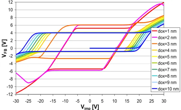
Fig. 1. presents simulated hysteresis curves as a function of oxide thickness. The hysteresis curves can be characterized with two main parameters. The horizontal width (devided by 2) indicates the avarage pulse amplitude necessary for recharging the structure at the given pulse width. The vertical width of the hysteresis is connected to the highest amount of charge that can be stored in the structure. It determines the highest width of the memory window for the given structure and pulse width.
Increasing the oxide thickness from 1 nm to 2 nm, the obtained hysteresis curve indicates increasing highest
amount of charge in the structure for a little lower charging voltages. But increasing the oxide thickness further, the amount of possible stored charge decreases fast, while the pulse amplitude necessary for recharging increases. From 4 nm up to 10 nm the highest possible amount of charge does not change further, while the pulse amplitude increases slowly. It is connected to the change of charge injection mechanism from direct to Fowler- Nordheim tunneling.
These results are in agreement with the results of our earlier calculations [16]. Studying the effect of oxide thickness on the tunnelling probability at different electric fields it was concluded that the optimal oxide thickness is 2-3 nm [16]. The simulation of hysterezis curves indicates an optimal oxide thickness about 2 nm.
The results obtained here are in agreement with our experimental results as well, which were obtained in MNOS structures with and without Si [8] or Ge nanocrystals [9,10]. MNOS structures with different oxide thicknesses were studied, and the best charging behaviour were obtained for an oxide thickness of about 2 nm.
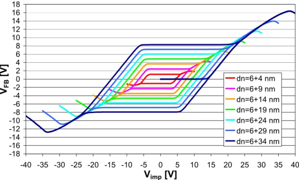
The effect of nitride thickness can be seen in Figs. 2 and 3. Fig. 2 presents the hysteresis curves obtained for the case when the charge centroid is a 1/5 part of the total nitride thickness, while hysteresis curves presented in Fig. 3 are obtained for a fixed charge centroid of 6 nm. In the first case the shape of hysteresis curves is similar, both the horizontal and vertical width decrease proportional to the decreasing nitride thickness. But in the case of a fixed depth of charge centroid the vertical width of the hysteresis decreases faster than the horizontal width. This case is closer to reality. So, in real cases the memory window shrinks faster with decreasing nitride thickness, than the charging pulse amplitude decreases. Therefore, a thin nitride layer decreases the efficiency of the injected charge. One should make a compromise between the low charging pulse amplitude and the memory window width.
The effect of the depth of charge centroid has also been studied. It was obtained that for the same voltage pulse amplitude the flat-band voltage decreases linearly with inreasing depth of charge centroid, as can be seen in Fig. 4. So, the possible memory window width decreases monotonically with increasing depth of charge centroid.
Therefore, for optimal charging behaviour the depth of injected charge centroid should be minimized. However, it is rather complicated to influence the depth of charge centroid by technology, on one hand. On the other hand, the retention time (the long of information storage) is better for deeper location of the injected charge [18]. So, if even one can influence the location of charge centroid, he has to make a compromise between the memory window width and retention time.
-18 -16 -14 -12 -101012-8-6-4-202468 1416 18
-40 -35 -30 -25 -20 -15 -10 -5 0 5 10 15 20 25 30 35 40
V
imp[V]
V
FB[V]
dn=2+8 nmdn=3+12 nm dn=4+16 nm dn=5+20 nm dn=6+24 nm dn=7+28 nm dn=8+32 nm
Figure 2. Simulated hysteresis curves as a function of nitride thickness in the range of 10-40 nm. The oxide thickness is 2 nm, the depth of charge centroid is 1/5 part of the total nitride thickness, the pulse width is 10 ms. The voltage pulse amplitude is
increased or decreased by 1 V step by step.
-12 -10 -8 -6 -4 -2 0 2 4 6 8 10 12
-30 -25 -20 -15 -10 -5 0 5 10 15 20 25 30
V
imp[V]
V
FB[V ]
dox=1 nm dox=2 nm dox=3 nm dox=4 nm dox=5 nm dox=6 nm dox=7 nm dox=8 nm dox=9 nm dox=10 nm
Figure 1. Simulated hysteresis curves as a function of oxide thickness in the range of 1-10 nm. The nitride thickness is 30 nm, the depth of charge centroid is 6 nm, the pulse width is 10 ms.The hysteresis curves are begun to be calculated from zero pulse
amplitude and zero flat-band voltage. The voltage pulse amplitude is increased or decreased by 1 V step by step.
-18-16 -14-12 -101012141618-8-6-4-202468
-40 -35 -30 -25 -20 -15 -10 -5 0 5 10 15 20 25 30 35 40
V
imp[V]
V
FB[V]
dn=5+35 nmdn=10+30 nm dn=15+25 nm dn=20+20 nm dn=25+15 nm dn=30+10 nm dn=35+5 nm
Figure 4. Simulated hysteresis curves as a function of depth of charge centroid from the oxide/nitride interface in the range of 5-35 nm. The oxide thickness is 2 nm, the nitride thickness is 30 nm, the pulse width is 10 ms. The voltage pulse amplitude is
increased or decreased by 1 V step by step.
-18 -16 -14 -12 -101012141618-8-6-4-202468
-40 -35 -30 -25 -20 -15 -10 -5 0 5 10 15 20 25 30 35 40
V
imp[V]
V
FB[V ]
dn=6+4 nm dn=6+9 nm dn=6+14 nm dn=6+19 nm dn=6+24 nm dn=6+29 nm dn=6+34 nm
Figure 3. Simulated hysteresis curves as a function of nitride thickness in the range of 10-40 nm. The oxide thickness is 2 nm, the depth of charge centroid is 6 nm, the pulse width is 10 ms. The voltage pulse amplitude is increased or decreased by 1 V
step by step.
IV. CONCLUSIONS
MNOS memory hysteresis curves have been calculated.
The effect of the oxide and nitride thickness as well as the depth of charge centroid has been studied. It has been concluded that the optimal oxide thickness is about 2 nm, in agreement with experimental results. The decrease of nitride thickness decreases the efficiency of the injected charge. Choosing the nitride thickness one makes a compromise between the low charging pulse amplitude and the memory window width. It has also been obtained that the possible highest memory window width decreases monotonically with increasing depth of charge centroid.
ACKNOWLEDGMENT
The authors gratefully acknowledge the grant provided by the project TÁMOP-4.2.2/B-10/1-2010-0020, Support of the scientific training, workshops, and establish talent management system at the Óbuda University.
REFERENCES
[1] P. Normand, E. Kapetanakis, P. Dimitrakis, D. Skarlatos, K.
Beltsios, et al. "Nanocrystals manufacturing by ultra-low-energy ion-beam synthesis for non-volatile memory applications", Nucl.
Instr. and Meth. B, 216, 228-238, 2004, and references therein.
[2] P. Dimitrakis, E. Kapetanakis, D. Tsoukalas, D. Skarlatos, C.
Bonafos, et al., "Silicon nanocrystal memory devices obtained by ultra-low-energy ion-beam synthesis", Solid-State Electron., 48, (9), 1511-1517, 2004.
[3] B. De Salvo, C. Gerardi, R. van Schaijk, S. A. Lombardo, D.
Corso, et al., "Performance and Reliability Features of Advanced Nonvolatile Memories Based on Discrete Traps (Silicon Nanocrystals, SONOS)", IEEE Trans. Dev. Mater. Reliability, 4, (3), 377-389, 2004, and references therein.
[4] B. Pődör, Zs. J. Horváth, P. Basa (Eds.), "Semiconductor Nanocrystals; Proc. First Int. Workshop on Semiconductor Nanocrystals SEMINANO2005, Sept. 10-12, 2005, Budapest, Hungary" Vols. 1 and 2.
[5] Zs. J. Horváth, "Semiconductor nanocrystals in dielectrics:
Optoelectronic and memory applications of related silicon based MIS devices", Current Appl. Phys., 6, (2), 145-148, 2006, and references therein.
[6] C.L. Heng, N.W. Teo, Vincent Ho, M.S. Tay, Y. Lei, et al.,
"Effects of rapid thermal annealing time and ambient temperature on the charge storage capability of SiO/pure Ge/rapid thermal oxide memory structure", Microel. Eng., 66, 218-223, 2003.
[7] A. Dana, I. Akca, O. Ergun, A. Aydinli, R. Turan, et al., "Charge retention in quantized energy levels of nanocrystals", Physica E, 38, (1-2), 94-98, 2007.
[8] Zs. J. Horváth, P. Basa, T. Jászi, A. E. Pap, L. Dobos, et al.,
"Electrical and memory properties of Si3N4 MIS structures with embedded Si nanocrystals", J. Nanosci. Nanotechnol., 8, 812, 2008.
[9] Zs. J. Horváth, P. Basa, "Nanocrystal non-volatile memory devices", Mater. Sci. Forum, 609, 1, 2009.
[10] Zs. J. Horváth, P. Basa, "Chapter 5: Nanocrystal memory structures" in: Nanocrystals and Quantum Dots of Group IV Semiconductors, (Eds. T. V. Torchynska, Yu. V. Vorobiev), American Scientific Publishers, 2010, 225.
[11] D. Frohman-Bentchkowsky, M. Lenzlinger, “Charge Transport and Storage in Metal-Nitride-Oxide-Silicon (MNOS) Structures,”
J. Appl. Phys. 40, (1969) 3307.
[12] K. I. Lundström, C. M. Svensson, “Properties of MNOS Structures,” IEEE Trans. El. Dev., ED-19 (1972) 826.
[13] Zs.J.Horváth, "Ocenka gisterezisa MNOP elementov pam'ati", Proc. 3rd Int. Sci. Coll. T.U. Ilmenau, Oct. 30 - Nov. 3, 1978, Ilmenau, GDR, Heft 7, 81.
[14] Zs.J.Horváth, "Memory hysteresis measurements on silicon oxynitride films", Solid-State Electron. 23, 1053-1054, 1980 [15] Zs. J. Horváth, V. Hardy, "Simulation of memory behaviour of
non-volatile structures", J. Nanosci. Nanotechnol., 8, 834–840, 2008.
[16] Zs. J. Horváth, K. Zs. Molnár, Gy. Molnár, P. Basa, T. Jászi, et al.,
“Charging behaviour of MNOS structures with embedded Ge nanocrystals,” phys. stat. sol. (c), in press, DOI:
10.1002/pssc.201100668.
[17] P. Basa, Zs. J. Horváth, T. Jászi, A. E. Pap, L. Dobos, et al.,
“Electrical and memory properties of silicon nitride structures with embedded Si nanocrystals,” Physica E, 38 (2007) 71.
[18] Zs. J. Horváth, K. Z. Molnár, "Retention behaviour of MNOS and SONOS memory structures with embedded semiconductor nanocrystals - a computer study", Progress in Applied Surface, Interface and Thin Film Science (SURFINT-SREN III), May 14- 19, 2012, Florence, Italy, in press.