Contents lists available atScienceDirect
Surface & Coatings Technology
journal homepage:www.elsevier.com/locate/surfcoat
Investigation of the ASPN process of low alloy steel by using Ni or Cr coated active screens
Dorina Kovács
a,⁎, János Dobránszky
b, Tamás Fodor
c, Viktor Takáts
c, Attila Bonyár
daBudapest University of Technology and Economics, Faculty of Mechanical Engineering, Department of Materials Science and Engineering, Műegyetem rkp. 3, 1111 Budapest, Hungary
bMTA–BME Research Group for Composite Science and Technology - ELKH, Műegyetem rkp. 3, 1111 Budapest, Hungary
cInstitute for Nuclear Research, Bem tér 18/c, 4026 Debrecen, Hungary
dBudapest University of Technology and Economics, Department of Electronics Technology, Egry József street 18, 1111 Budapest, Hungary
A R T I C L E I N F O Keywords:
Active screen plasma nitriding Coated screen
Secondary neutral mass spectrometry X-ray photoelectron spectroscopy Depth profiling
A B S T R A C T
The mechanism of active screen plasma nitriding (ASPN) and the influence of the active screen's coating material on the surface properties of the nitrided layer was investigated on low alloyed steel samples, using chromium or nickel-coated active screens. ASPN experiments were performed at 510 °C, for 5 h in a 75% N2+ 25% H2gas mixture using tempered 42CrMo4 type low alloy steel. The base material of the screens was unalloyed steel, but the screens were electroplated with chromium or nickel. Scanning electron microscopy (SEM), energy dispersive spectroscopy (EDS), X-ray diffractometry (XRD), atomic force microscopy (AFM), and secondary neutral mass spectrometry (SNMS) were used for the characterization of surface properties of the samples and the screen.
SNMS results show that the coating material of the active screen (chromium or nickel) was deposited on the surface of the samples in the form of compounds, with layer thicknesses between 160 and 200 nm (chromium) and 290–420 nm (nickel). Chemical analysis by X-ray photoelectron spectroscopy (XPS), performed at the in- terface of the steel sample and the deposited compounds reveals that iron-nitride was only formed in the case of samples that were treated with a Cr-coated active screen. Here the decomposition and oxidation of the unstable chromium-nitride provided the nitrogen atoms and the chemical drive for the formation of iron-nitride. In the case of the Ni-coated active screen, only molecular nitrogen was observed in the treated steel samples. The results prove that – contrary to widespread models on ASPN nitriding mechanisms – physically adsorbed ni- trogen plays little role in the nitriding process of iron.
1. Introduction
Tempered low alloy steels are often used for gears and shafts. These parts are usually exposed to wear and, in some cases, also to corrosion.
The effective way to improve the wear and corrosion resistance of these components is to modify the surface properties by the proper con- stitution of the diffusion layer and coating [1]. Different strategies have been utilized to improve the characteristics of the coating materials, including multilayer structures that are generated by depositing two or more alternative materials [2,3].
Active screen plasma nitriding (ASPN) is a widely used surface treatment process, which offers many advantages compared to the conventional direct current plasma nitriding, such as better layer uni- formity and the elimination of the edge effects [4,5]. In this process, the workpiece is surrounded by a conductive mesh screen (also called a
cage), which is on cathodic potential, while the furnace wall is kept on anodic potential [6,7]. In ASPN, the sample is usually either insulated from the high voltage source (and thus on a floating potential) or on a lower cathodic bias compared to the screen. Consequently, the ions of the plasma bombard and sputter the sample to a smaller extent com- pared to the screen. The sample is heated by radiation [8,9] and ne- cessarily by the plasma as well.
The surface hardening of steel specimens originates from the for- mation of a nitride compound layer on the surface and a nitrogen dif- fusion zone underneath it. The nitriding mechanisms used to describe the ASPN process differ significantly from the “sputtering of iron and re-condensation of iron-nitride” model of Köbel used for DC plasma nitriding [10]. In the first step of ASPN, according to the model offered by Zhao, the unalloyed steel surface of the active screen is covered by a thick compound layer containing Fe2e3N, Fe4N, in a mechanism similar
https://doi.org/10.1016/j.surfcoat.2020.125638
Received 15 January 2020; Received in revised form 6 March 2020; Accepted 12 March 2020
⁎Corresponding author at: Department of Materials Science and Engineering, Faculty of Mechanical Engineering, Budapest University of Technology and Economics, Műegyetem rakpart 3., Budapest 1111, Hungary.
E-mail address:dorina@eik.bme.hu(D. Kovács).
Available online 13 March 2020
0257-8972/ © 2020 The Authors. Published by Elsevier B.V. This is an open access article under the CC BY license (http://creativecommons.org/licenses/BY/4.0/).
T
to DCPN [11,12]. Consequently, iron-nitride particles will be sputtered from the screen, which passes through the plasma where they physi- cally and chemically adsorb the active nitrogen atoms before deposited on the surface of the steel sample [11,13,14]. In the model of Zhao, the formation of iron-nitride on the surface of the sample is driven by two processes. First, the physically adsorbed nitrogen atoms desorb on the surface due to the contact between the particles and the substrate surface and the high substrate temperature. The released nitrogen can either form molecular nitrogen and diffuse into the sample or form iron- nitride. Secondly, the decomposition of higher iron-nitrides, like the metastable FeN and Fe2e3N, release nitrogen, which can form further nitrides. In this modified model of “sputtering-adsorption-desorption,”
Zhao clearly considers the sputtered particles as the main nitrogen carriers in the active screen plasma nitriding process. The validity of this model can be tested by changing the material of the active screen:
regardless of the screen's material, the sputtered metal atoms and metal-nitrides carry physically and chemically absorbed nitrogen to the sample surface, which can catalyze the nitriding of iron. Thus, one of the aims of our work is to test the validity of this model and investigate the effect of the active screen's material on the ion nitriding process.
Besides, the deposited materials originating from the active screen (metals and nitrides) also modify the properties of the steel surface [15,16]. Generally – as investigated by others – the materials of both the screen and the sample influence the resulting surface properties in a complex way.
Naeem et al. [17] examined the distance between the active screen and the sample in which austenitic stainless steel screen was used to treat carbon steel samples. After the treatment, they measured in- creased chromium and nickel content on the surface of the samples.
This observation has inspired new research in which stainless steel and aluminum screens were used one after another to improve the surface properties. Aluminum nitride was found to be the main phase in sam- ples nitrided in this fashion, with and the hardness being much higher (1100 HV) than in samples treated conventionally (800 HV) [18].
Nishimoto et al. [19] used a titanium screen for nitriding high-alloyed steel. A TiN layer was formed on the surface by sputtering from the screen and by deposition of the nitrides.
In this manner, both the material of the active screen and sample can be examined. Yazdani et al. [20] nitrided aluminum sample with carbon steel screen. An iron-nitride layer was formed on the top of the sample surface. The authors stated that the nitrogen atoms diffused into the Al substrate and formed an AlN layer beneath the iron nitride coating at long coating periods, although this was not detected by XRD.
Taherkhani and Soltanieh [21] also used an iron screen on aluminum samples. The influence of nitriding time and temperature on the surface properties of coated aluminum alloy samples was investigated. A combination of AlN and Fe2e3N phases were shown to form by the ASPN process. The authors call this a composite nitride layer. If the nitriding time is long enough (≥11 h), a number of iron nitride parti- cles can be sputtered from the screen to be deposited on the surface, which will result in a desirably thicker coating with larger grain size [22].
EDS (energy dispersive spectrometry) analysis was preferably used for the determination of nitrogen content [17,23,24]. Besides this measurement, the GDOES (glow discharge optical spectrometry) is the most common depth profiling technique to analyze the chemical com- position of the layer [25–27]. Both the nitride layer of structural steel and the expanded austenite layer of the austenitic stainless steels can be characterized by this method. However, the nitrogen content of the diffusion zone cannot be analyzed by any measurement techniques.
Hosseini and Ashrafizadeh [28] were compared three types of compo- sitional depth profile analyzer techniques. Nitrogen is a light element with a relatively low concentration in a plasma nitrided layer; thus, it is difficult to be measured if only one of the conventional surface analysis techniques is employed. A 6 μm thick layer was presented in this study.
In this case, EDS provided more accurate values for the N content than
GDOES, since the latter predicted an only 4.5 μm thick layer. It should be noted that GDOES does not give direct distance information; there- fore, it needs a very precise correspondence of the sputtering time to sputtering depth. SIMS (secondary ion mass spectrometry) was used to determine the N content in the diffusion zone. Quantitative results were not presented, only the profile of the measurements, but the results were validated by N content calculation [29]. SNMS (secondary neutral mass spectrometry) was rarely used to investigate the nitrided layer [30]. Galesic and Kolbesen [31] showed the changes of V and N in the function of the sputtering time, but the depth was not calculated. In contrast, Jauberteau et al. [32] found MoO2, MoO3compounds after the nitriding, but N also could diffuse into the metal in a hundred nm, which can be seen in the SNMS profile.
Conclusively, the aim of our research is to investigate the nitriding process of steel and the chemical composition of the formed nitride layer (with SNMS and XPS), using nickel or chromium coated screens for ASPN, with relation to the widely used nitriding models.
Furthermore, the self-nitriding of the coated active screen was also investigated. Information regarding the processes on the active screen's surface during plasma nitriding cannot be found in the literature.
2. Material and methods 2.1. Sample preparation
Tempered 42CrMo4 grade steel was used as a substrate material in this study. The material was cut into disks with a 20 mm diameter and 6 mm thickness. The samples were wet ground by using silicon carbide papers of multiple grit sizes and later polished by diamond suspension, then degreased in an ultrasonic vibrated acetone bath and dried with air directly before the nitriding process.
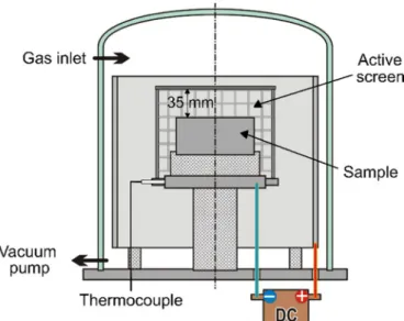
Fig. 1.Illustration of the used plasma nitriding equipment.
Table 1
Designation and details of the various ASPN treatments. One screen (either nickel or chromium coated) was used for two samples consecutively; this is referred to as the first and second ASPN in the table.
Designation Treatment
PNi1x First ASPN with the nickel coated screen
PNi2x Second ASPN with the nickel coated screen
PCr1x First ASPN with the chromium coated screen
PCr2x Second ASPN with the chromium coated screen
D. Kovács, et al. Surface & Coatings Technology 394 (2020) 125638
2.2. Plasma nitriding
The base material of the screens was made from a 1.0330 type non- alloyed quality steel. The dimensions of the screen were
∅140 × 85 × 0.8 mm. Two coating materials were electroplated in an industrial bath: nickel and chromium. For the chromium coating, chromic acid, for the nickel coating Watts-electrolyte were used ac- cording to well-known protocols [33,34].
The samples were nitrided for 5 h at 510 °C using 75% N2+ 25% H2
gas mixture. The gas pressure was kept constant at 280 Pa. The sample was placed at the center of the active screen, 35 mm from the top lid.
The temperature was monitored by using an isolated K-type thermo- couple mounted directly under the workpiece. The illustration of the equipment can be seen inFig. 1. After the nitriding, the samples were cooled down under the operating gas to 250 °C. Afterwards; they were cooled down to room temperature when the chamber was pressurized with air.
All treatments were carried out by using the same plasma nitriding parameters. One screen was used for two different specimens as an active screen. Both the diffusion of the coating material into the
substrate and the changing of the screen's surface were investigated.
Table 1 shows the experimental treatments which were used on the samples and their designation.
2.3. Characterization methods
The surfaces of the nitrided samples were analyzed by XRD with theta-2 theta vertical goniometer and Cu target. The scan parameters were: 40–80° in 2 theta, the wavelength was 1.54 nm, while the ex- posure time was set to 0.04 s/step. Surface morphology, the cross-sec- tion, and the elemental composition of the screen surface were in- vestigated by using a Zeiss EVO MA10 scanning electron microscope along with EDS. Hardness was measured by a Buehler IndentaMet 1105 type Vickers microhardness tester by using 10 g load. To measure the surface morphology, a Veeco diInnova type atomic force microscope (AFM) was used in contact-mode with an ART D160 diamond probe (spring constant: 5 N/m). The images were obtained in 10 μm × 10 μm scan sizes, with a sampling resolution of 512 × 512 and 1 Hz scan rate.
The obtained images were post-processed with the Gwyddion 2.36 software [35].
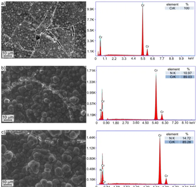
Fig. 2.SEM images of the screens' surface and corresponding EDS spectra. The screens were used a) 0 time, b) 1 time, c) 2 times with Cr-coated screen, and d) 0 time, e) 1 time, f) 2 times with Ni-coated screen.
In SNMS analysis, the sample surface was bombarded by ions, and the sputtered neutral particles were detected after ionization, i.e., the sputtering and ionization were strictly separated from each other [36].
The main characteristic feature of SNMS and its advantage is the se- paration between emission and ionization of particles, which results in a matrix-independent method. The surface bombardment and post io- nization were performed by low-pressure Electron Cyclotron Wave Resonance (ECWR) argon plasma. Due to the presence of a surface oxide layer on the samples, the SNMS was operated in a high-frequency mode, which ensured an effective charge compensation against surface charge accumulation resulting in inhomogeneous ion bombardment. A sputtering potential of 350 V at 100 kHz frequency with 80% duty cycle was applied. The investigated area was confined within a circle of 3 mm diameter by a tantalum mask. The lateral homogeneity of ion bom- bardment was checked by measuring the shape of the sputtered crater with an AMBIOS XP-1 type profilometer. The profilometer was also used to determine the sputtering rate by measuring the crater depth as a function of sputtering time, and to measure the surface roughness parameters. XPS measurements were performed at different depths of interest, depending on the treated sample. For this purpose, samples were transported under UHV conditions from the SNMS chamber to the XPS, i.e., without exposing samples to air. As XPS gives both
quantitative and qualitative information about the sample surface, elemental composition and chemical environment can be examined. An XPS equipped by Al/Mg twin anode non-monochromatized X-ray source and Phoibos 100 MCD-5 series hemispherical energy analyzer produced by Specs was used. Electron states were excited by aluminum Al Kα X-ray source (with excitation energy 1486.6 eV and line width 0.86 eV). The elemental composition was obtained from a single region spectra with 10 eV pass energy. All binding energies were referenced to the freshly sputtered Au 4f7/2 peak at 84.0 eV binding energy. The intensities were calculated from the peak areas by fitting in the CasaXPS program [37].
3. Results and discussion
3.1. Surface characterization of the coated screens
Fig. 2shows the morphology of the chromium- and nickel-coated screens. The composition of the screens was controlled by SEM-EDS area analysis before each treatment. 100% Cr or Ni appropriately was measured on the coated screens surface, which means that the substrate material of the screen was perfectly masked. It can be observed in Fig. 2a and d, that the chromium coating contained microcracks while Fig. 2. (continued)
D. Kovács, et al. Surface & Coatings Technology 394 (2020) 125638
the nickel coating was smooth. During nitriding, the surface mor- phology of both screens changed. Ions from the plasma bombarded the biased screen directly, so its surface also became nitrided. Due to bombardment with nitrogen ions, after the first nitriding, a grainy surface structure was formed, which is especially well visible inFig. 2b and e compared to the original surface. Repeating the ASPN process, the general morphological character of the surface texture did not change significantly, but the areal attributes (as defined by the ISO 25178-2 standard) changed very clearly (Fig. 2c and f).
The presence of nitrogen – which is higher in the case of the chro- mium covered screen – indicates either the formation of nitrides or embedded molecular nitrogen. It has to be noted that the formed nitride layer on top of the screen is exposed to constant sputtering by the ions, which removes and re-deposits parts of the nitride layer. Probably this mechanism caused the porous structure of the nickel screen, well
observable inFig. 2e and f. Another interesting difference between the two screens is the appearance of iron on the nickel covered screen after the ASPN cycles. This iron is supposedly sputtered and deposited here either from the sample or from uncovered parts of the equipment.
Fig. 3shows the cross-section of the active screens. The average thickness of the chromium coating is 30 μm, the nickel layer is 75 μm.
The nitrided parts of the layers cannot be distinguished based on these cross-sectional images. The progression of the cracks – which were al- ready present prior to the first process, as can be seen inFig. 2a – in the chromium layer during the subsequent ASPN steps is visible inFig. 3a, b, c. During nitriding, this layer became more brittle, which can be caused by the formation of the Cr-nitride. The porosity of the nickel layer is clearly visible inFig. 3e and f. A slight increase in the porosity can be observed as an effect of the second nitriding process.
Fig. 3.Cross-section SEM images of the a) 0 time, b) 1 time, c) 2 times used Cr-coated screen and d) 0 time, e) 1 time, f) 2 times used Ni coated screen.
3.2. Surface characterization of the samples
After nitriding, the appearance of the sample surface remained po- lished as it was at the end of the preparation. This can be considered quite unusual since the nitriding process generally causes a matte, grey discoloration on the surface [38,39]. The typical white layer [40,41]
was not formed on any of the surfaces. The original tempered micro- structure was retained after the plasma nitriding.
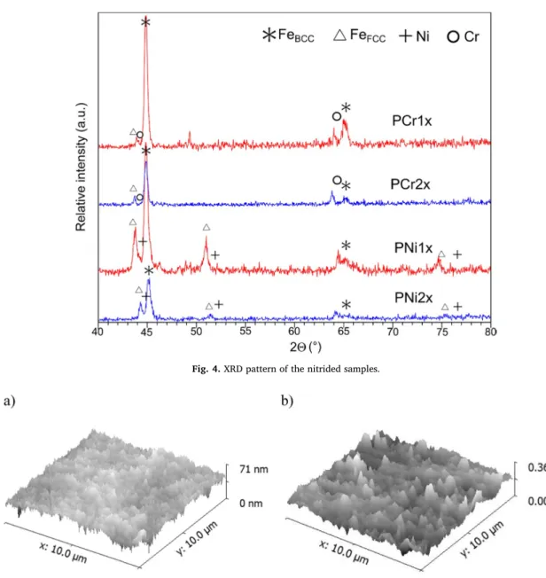
It can be seen in the XRD patterns ofFig. 4that the main phase is alpha‑iron, which has a body-centered cubic crystal structure. Besides this phase, another form of the iron was found, which has a face-cen- tered cubic structure corresponding to austenite. These phases can be observed on both samples, which were nitrided by the nickel screen.
The nitridation process did not cause the hardening of the steel. The hardness rates were within the deviation of the base material, 420 HV0.01 ± 45.
The lattice constant of the FCC phase was 3.85 Å, which decreased in PNi2x, and the peaks of Ni also appeared, as can be seen inFig. 4. In contrast, the samples which were nitrided by the chromium screen had a different reaction to the process. Only the BCC iron phase can be detected clearly in both samples, but the lattice constant of this phase was also decreased. Neither iron nitride nor chromium nitride was
formed on the surface.
SNMS depth profiling was used to analyze the elemental composi- tion in the function of the depth from the sample surface. The depth profiles characterize the distribution of the main elements originating from the base material and the screen. Nitrogen was investigated se- parately by XPS, especially at the interfaces of the layered structure, e.g., between the deposited coating element and the iron. For this purpose, the SNMS measurements were interrupted at the required stages. AFM was used to analyze the morphology of the surface before previous measurements.
Fig. 5presents of contact-mode AFM images made on the samples.
As can be seen, the maximum distance between the highest and lowest points on the sample surface increased from 71 nm to 360 nm between the first and second nitriding process. The surface roughness (Sa) in- creased from 4.7 nm to 30.6 nm. The differences were caused by the increased amount of deposited coating elements.
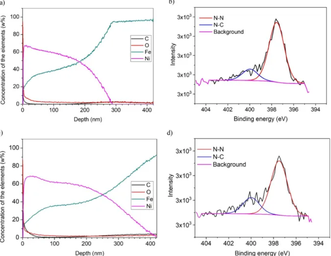
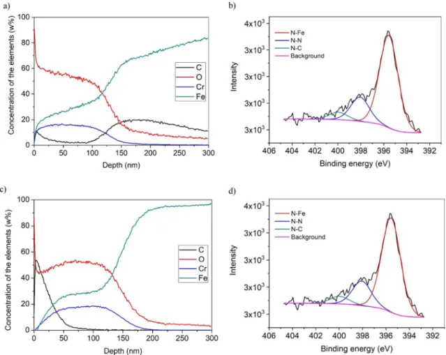
As can be seen inFig. 6a and c, Ni was deposited on the surface of both samples, which were treated by a Ni-coated screen. According to the XPS results presented inFig. 7b and d, FeeN bonds were not de- tected, which proves that iron nitride was not formed during the pro- cess. The depth of the diffused layer was 291 nm in the PNi1x and 421 nm in the PNi2x sample. Only molecular nitrogen was found in this Fig. 4.XRD pattern of the nitrided samples.
Fig. 5.3D contact-mode AFM images of a) 1 time, b) 2 times nitrided samples with Ni-coated screen.
D. Kovács, et al. Surface & Coatings Technology 394 (2020) 125638
measured depth at the interface (Fig. 6b and d). According to the porous surface morphology, the molecular nitrogen, which came from the nitriding gas, could be stuck in the pores and voids during the layer deposition.
SNMS depth profiles of the samples treated by the Cr-coated screen are shown inFig. 7a and c. As can be seen, the curves corresponding to Cr and O have a similar profile, which suggests the presence of chro- mium-oxide in the layer. The gas mixture that was used for the process is free from oxygen, and the amount of oxygen in the layer is much more than what could be expected as remaining in the chamber. This oxide layer was most probably formed during the flushing of the chamber with air after the end of the nitriding process. Although in the nitrogen plasma chromium-nitride was deposited on the surface of the sample, the formed CrN and Cr2N compounds are not stable and easily oxidize to Cr2O3in the presence of oxygen and on high temperature [42] – which conditions are true while flushing the still hot sample with air. The XPS diagrams (Fig. 7b and d) also show high FeeN content below the chromium-rich layer, although it was not detected by XRD on the surface. It means iron-nitride could be formed on the interface of iron and chromium oxide. The characteristic of the depth profile dia- grams is the same for both samples. The thickness of the chromium oxide layer in the PCr1x sample was 167 nm, in the PCr2x sample, was 198 nm. Although the scale of the XPS diagrams ends at 300 nm, the chromium profile already decreased to zero before that, which means that the chromium could not diffuse into the substrate.
Fig. 8presents SEM-EDS maps and shows the distribution of Fe, N, Cr, Ni elements in the cross-section of the samples. Since the formed layer thicknesses were similar in both cases (with both plating mate- rials), only two samples are presented inFig. 8. Copper support was
used for the grinding, to avoid damaging the deposited layers. The EDS maps confirm our previous observations: the Ni layer is thicker com- pared to the Cr. Unfortunately, the N content of the samples cannot be evaluated with this detector.
These results also shed new light on the accepted nitriding models, which place great emphasis on the sputtered particles from the screen as the main carriers of nitrogen for the nitriding of steel on the sample surface. As previously discussed, by using a pure steel active screen, the sputtered higher iron-nitride (Fe1e3N) particles carry physically and chemically adsorbed nitrogen to the steel surface [10]. In the model, the nitriding of the iron on the surface is fuelled by both the desorbed nitrogen atoms and also the decomposition of the higher metastable nitrides. The surfaces of both the Cr and Ni electroplated screens are nitrided during the ASPN process. Thus chromium- and nickel-nitrides are sputtered and subsequently deposited on the surface of the steel samples. In both cases, the sputtered nitride particles can carry the physically adsorbed nitrogen to the surface, similar to the model with iron-nitride particles. However, the desorption of adsorbed nitrogen from these particles did not lead to the direct formation of iron-nitride.
In the case of nickel, only molecular nitrogen was found without any trace of iron-nitride. In the case of chromium, iron-nitride was found on the interface, where the decomposition and oxidation of chromium- nitride provided the nitrogen and chemical drive for the nitriding of iron. The fact that physically adsorbed nitrogen is available in both cases and that iron-nitride was not observed in the case of nickel proves that the chemical decomposition was the main driving force of iron nitriding. The nickel-nitride is more stable exposed to oxygen (con- firmed by the lack of oxides based on the SNMS results) and seems to retain its chemically bound nitrogen.
Fig. 6.Characteristic of the a) PNi1x by SNMS, b) PNi1x by XPS, c) PNi2x by SNMS, d) PNi2x by XPS measurements.
Fig. 7.Characteristic of the a) PCr1x by SNMS, b) PCr1x by XPS, c) PCr2x by SNMS, d) PCr2x by XPS measurements.
Fig. 8.EDS elemental maps made on the PCr2x and PNi2x samples along their cross-section.
D. Kovács, et al. Surface & Coatings Technology 394 (2020) 125638
Our observations also offer suggestions to refine the model of the ASPN process in the classical case, when a pure steel active screen is used. After the initial deposition of iron-nitrides on the sample surface, the subsequent development of nitriding is primarily driven by the decomposition of the higher-nitrides to lower nitrides (from Fe1e3N to Fe4N), which release chemically active nitrogen atoms to the sur- rounding steel matrix. The effect of physically adsorbed and later des- orbed nitrogen is much lower since iron-nitride cannot be found on nitrided samples, where only physically released nitrogen was present (such as in the case of an active screen electroplated with nickel).
4. Conclusion
The material of the active screen is a major parameter that influ- ences the outcome of the nitriding process. In this study, nickel or chromium covered active screens were used to investigate this effect on nitrided steel samples. ASPN was performed at 510 °C for 4 h in a gas mixture containing 75% N2 and 25% H2. With these process para- meters, Ni was detected on the surface of the treated samples in a de- posited layer with several hundreds of nanometres thickness. However, iron-nitride was not formed on the surface, and only molecular nitrogen was found on the interface of nickel and iron. After the nitriding with the Cr coated screen, mostly Cr2O3was formed on the surface with an average thickness of 170 nm. At the interface, FeeN bonds were found, which indicate that low amounts of iron-nitride could be created with the own Fe content of the substrate.
The results point out that the role of physically adsorbed and sub- sequently desorbed nitrogen by the sputtered particles is overestimated in the previous ASPN models. Iron nitriding was only observed when the chemical decomposition of other nitrides provided reactive nitrogen atoms to the steel matrix, such as the interface of chromium‑iron.
CRediT authorship contribution statement
Dorina Kovács:Investigation, Methodology, Writing - original draft, Visualization.János Dobránszky:Conceptualization, Supervision.Tamás Fodor:Investigation.Viktor Takáts:
Investigation.Attila Bonyár:Investigation, Writing - review &
editing.
Declaration of competing interest
The authors declare that they have no known competing financial interests or personal relationships that could have appeared to influ- ence the work reported in this paper.
Acknowledgments
The authors are grateful to the foundation of Richter Gedeon Talentum for supporting this research. The research reported in this paper was supported by the Higher Education Excellence Program of the Ministry of Human Capacities in the frame of Nanotechnology re- search area of Budapest University of Technology and Economics (BME FIKP-NAT) and also supported by the National Research, Development, and Innovation Fund (TUDFO/51757/2019-ITM, Thematic Excellence Program).
References
[1] S. Goldež, M. Podgrajšek, B. Podgornik, Z. Ren, The influence of PVD coating on the low cycle fatigue behaviour of Cr-Mo-V steel at elevated temperatures, Surf.
Coatings Technol. 321 (2017) 358–365,https://doi.org/10.1016/j.surfcoat.2017.
05.008.
[2] R. Bayón, A. Igartua, X. Fernández, R. Martínez, R.J. Rodríguez, J.A. García, A. de Frutos, M.A. Arenas, J. de Damborenea, Corrosion-wear behaviour of PVD Cr/CrN multilayer coatings for gear applications, Trib. Int 42 (2009) 591–599,https://doi.
org/10.1016/j.triboint.2008.06.015.
[3] J.A.M. Ferreira, J.D.M. Costa, V. Lapa, Fatigue behaviour of 42CrMo4 with PVD coating, Int. J. Fatigue 19 (1997) 293–299,https://doi.org/10.1016/S0142- 1123(97)00007-8.
[4] R.R.M. de Sousa, F.O. de Araújo, J.A.P. da Costa, A. de S. Brandim, R.A. de Brito, C. Alves, Cathodic cage plasma nitriding: an innovative technique, J. Metall. 2012 (2012) 1–6,https://doi.org/10.1155/2012/385963.
[5] L. Wang, Y. Li, X. Wu, Plasma nitriding of low alloy steels at floating and cathodic potentials, Appl. Surf. Sci. 254 (2008) 6595–6600,https://doi.org/10.1016/j.
apsusc.2008.04.027.
[6] C.X. Li, Active screen plasma nitriding – an overview, Surf. Eng. 26 (2010) 135–141,https://doi.org/10.1179/174329409X439032.
[7] C.X. Li, J. Georges, X.Y. Li, Active screen plasma nitriding of austenitic stainless steel, Surf. Eng. 18 (2002) 453–457,https://doi.org/10.1179/
026708402225006240.
[8] Y. Li, Y. He, J.J. Xiu, W. Wang, Y.J. Zhu, B. Hu, Wear and corrosion properties of AISI 420 martensitic stainless steel treated by active screen plasma nitriding, Surf.
Coatings Technol. 329 (2017) 184–192,https://doi.org/10.1016/j.surfcoat.2017.
09.021.
[9] S. Ahangarani, F. Mahboubi, A.R. Sabour, Effects of various nitriding parameters on active screen plasma nitriding behavior of a low-alloy steel, Vacuum 80 (2006) 1032–1037,https://doi.org/10.1016/j.vacuum.2006.01.013.
[10] D. Pye, Practical Nitriding and Ferritic Nitrocarburizing, ASM International, Russell Township, OH, 2003.
[11] C. Zhao, C.X. Li, H. Dong, T. Bell, Study on the active screen plasma nitriding and its nitriding mechanism, Surf. Coatings Technol. 201 (2006) 2320–2325,https://doi.
org/10.1016/j.surfcoat.2006.03.045.
[12] A. Saeed, A.W. Khan, F. Jan, M. Abrar, M. Khalid, M. Zakaullah, Validity of
“sputtering and re-condensation” model in active screen cage plasma nitriding process, Appl. Surf. Sci. 273 (2013) 173–178,https://doi.org/10.1016/j.apsusc.
2013.02.008.
[13] P. Hubbard, J.G. Partridge, E.D. Doyle, D.G. McCulloch, M.B. Taylor, S.J. Dowey, Investigation of nitrogen mass transfer within an industrial plasma nitriding system I: the role of surface deposits, Surf. Coatings Technol. 204 (2010) 1145–1150, https://doi.org/10.1016/j.surfcoat.2009.08.029.
[14] P. Hubbard, S.J. Dowey, J.G. Partridge, E.D. Doyle, D.G. McCulloch, Investigation of nitrogen mass transfer within an industrial plasma nitriding system II: applica- tion of a biased screen, Surf. Coatings Technol. 204 (2010) 1151–1157,https://doi.
org/10.1016/j.surfcoat.2009.08.030.
[15] A. Nishimoto, T. Fukube, T. Tanaka, Effect of surface deposits on nitriding layer formation of active screen plasma nitriding, Mat. Trans. 57 (2016) 1811–1815, https://doi.org/10.2320/matertrans.M2016209.
[16] K. Lin, X. Li, H. Dong, P. Guo, D. Gu, Nitrogen mass transfer and surface layer formation during the active screen plasma nitriding of austenitic stainless steels, Vac 148 (2018) 224–229,https://doi.org/10.1016/j.vacuum.2017.11.022.
[17] M. Naeem, M. Sha, M. Zaka-ul-islam, A. Ashiq, J.C. Díaz-Guillén, M. Shahzad, M. Zakaullah, Enhanced surface properties of plain carbon steel using plasma ni- triding with austenitic steel cathodic cage, Mater. Des. 108 (2016) 745–753, https://doi.org/10.1016/j.matdes.2016.07.044.
[18] M. Naeem, M. Shafiq, M.I. Bashir, M. Zakaullah, Novel duplex cathodic cage plasma nitriding of non-alloyed steel using aluminum and austenite steel cathodic cages, J.
Alloys Compd. 721 (2017) 307–311,https://doi.org/10.1016/j.jallcom.2017.06.
[19] A. Nishimoto, H. Nii, R. Narita, K. Akamatsu, Simultaneous duplex process of TiN004.
coating and nitriding by active screen plasma nitriding, Surf. Coat. Technol. 228 (2012) 558–562,https://doi.org/10.1016/j.surfcoat.2012.04.021.
[20] A. Yazdani, M. Soltanieh, H. Aghajani, Active screen plasma nitriding of Al using an iron cage: characterization and evaluation, Vacuum 122 (2015) 127–134,https://
doi.org/10.1016/j.vacuum.2015.09.018.
[21] K. Taherkhani, M. Soltanieh, Investigation of nanomechanical and adhesion beha- vior for AlN coating and AlN/Fe2-3N composite coatings created by active screen plasma nitriding on Al 1050, J. Alloys Compd. 783 (2019) 113–127,https://doi.
org/10.1016/j.jallcom.2018.12.282.
[22] K. Taherkhani, M. Soltanieh, Composite coatings created by new method of active screen plasma nitriding on aluminium alloy 6061, J. Alloys Compd. 741 (2018) 1247–1257,https://doi.org/10.1016/j.jallcom.2017.12.360.
[23] Z. Keresztes, D. Pammer, P.J. Szabó, EBSD examination of argon ion bombarded ti- 6Al-4V samples produced with DMLS technology, Per. Pol. Mech. Eng. 63 (2019) 195–200,https://doi.org/10.3311/PPme.13821.
[24] J.E. Maróti, D. Károly, D.M. Kemény, Effects of additive manufacturing on the mechanical and corrosion properties of austenic stainless steel, Act. Mat. Trans. 2 (2019) 55–60,https://doi.org/10.33924/amt-2019-01-09.
[25] Z. Zhang, X. Li, H. Dong, Response of a molybdenum alloy to plasma nitriding, Int.
J. Refract. Met. Hard Mater. 72 (2018) 388–395,https://doi.org/10.1016/j.
ijrmhm.2018.01.014.
[26] E. Zdravecká, J. Slota, P. Solfronk, M. Kolnerová, Evaluation of the effect of dif- ferent plasma-nitriding parameters on the properties of low-alloy steel, J. Mater.
Eng. Perform. 26 (2017) 3588–3596,https://doi.org/10.1007/s11665-017-2787-3.
[27] S.R. Hosseini, F. Ashrafizadeh, Accurate measurement and evaluation of the ni- trogen depth profile in plasma nitrided iron, Vacuum 83 (2009) 1174–1178, https://doi.org/10.1016/j.vacuum.2009.03.006.
[28] S.R. Hosseini, F. Ashrafizadeh, Compositional depth profile investigation of plasma nitriding by multiple analyses techniques, Vaccum 85 (2011) 920–926,https://doi.
org/10.1016/j.vacuum.2011.01.011.
[29] S.R. Hosseini, F. Ashrafizadeh, A. Kermanpur, Calculation of compositional dis- tribution in nitrided iron by analytical modelling, Surf. Science and Eng. 8 (2010) 13–23.
[30] M. Godzsák, G. Lévai, K. Vad, A. Csik, J. Hakl, T. Kulcsár, G. Kaptay, Coloring hot- dip galvanization of steel samples in industrial zinc-manganese baths, Journal of Mining and Metallurgy, Section B: Metallurgy 53 (2017) 319–326,https://doi.org/
10.2298/JMMB170531028G.
[31] I. Galesic, B.O. Kolbesen, Formation of vanadium nitride by rapid thermal proces- sing, Solid Film 349 (1999) 14–18.
[32] I. Jauberteau, T. Merle-Méjean, S. Touimi, S. Weber, A. Bessaudou, A. Passelergue, J.L. Jauberteau, J. Aubreton, Expanding microwave plasma process for thin mo- lybdenum films nitriding: nitrogen diffusion and structure investigations, Surf.
Coatings Technol. 205 (2011) S271–S274,https://doi.org/10.1016/j.surfcoat.
2011.03.056.
[33] M. Soltanieh, H. Aghajani, F. Mahboubi, Kh.A. Nekouee, Surface characterization of multiple coated H11 hot work tool steel by plasma nitriding and hard chromium electroplating processes, Vac 86 (2012) 1470–1476,https://doi.org/10.1016/j.
vacuum.2012.01.003.
[34] N.A. Badarulzaman, A.A. Mohamad, S. Puwadaria, Z.A. Ahmad, The evaluation of nickel deposit obtained via Watts electrolyte at ambient temperature, J. Coat.
Technol. Res. 7 (2010) 815–820,https://doi.org/10.1007/s11998-010-9271-4.
[35] D. Nečas, P. Klapetek, Gwyddion: an open-source software for SPM data analysis, J.
Phys. 10 (2012) 181–188.
[36] K. Vad, A. Csik, G.A. Langer, Secondary neutral mass spectrometry-a powerful
technique for quantitative elemental and depth profiling analyses of nanostructures, Spectrosc. Eur. 21 (2009) 13–16.
[37] J.F. Moulder, W.F. Stickle, P.E. Sobol, K.D. Bomben, Handbook of X-Ray Photoelectron Spectroscopy: A Reference Book of Standard Spectra for Identification and Interpretation of XPS Data, Physical Electronics, Eden Prairie, MN, 1995.
[38] C. Alves, F.O. de Araújo, K.J.B. Ribeiro, J.A.P. da Costa, R.R.M. Sousa, R.S. de Sousa, Use of cathodic cage in plasma nitriding, Surf. Coatings Technol. 201 (2006) 2450–2454,https://doi.org/10.1016/j.surfcoat.2006.04.014.
[39] A. Nishimoto, A. Tokuda, K. Akamatsu, Effect of through cage on active screen plasma nitriding properties, Mater. Trans. 50 (2009) 1169–1173,https://doi.org/
10.2320/matertrans.MRA2008431.
[40] I. Hacisalihoglu, F. Yildiz, A. Alsaran, Wear performance of different nitride-based coatings on plasma nitrided AISI M2 tool steel in dry and lubricated conditions, Wear. 384–385 (2017) 159–168,https://doi.org/10.1016/j.wear.2017.01.117.
[41] L. Kenéz, N. Kutasi, E. Filep, L. Jakab-Farkas, L. Ferencz, Anodic plasma nitriding in hollow cathode (HCAPN), HTM - J. Heat Treat. Mater. 73 (2018) 96–105,https://
doi.org/10.3139/105.110344.
[42] A. Fabrizi, M. Cabibbo, R. Cecchini, S. Spigarelli, C. Paternoster, M. Haidopoulo, Ph.V. Kiryukhantsev-Korneev, Thermal stability of nanostructured coatings, Mat.
Sc. For. 653 (2010) 1–22,https://doi.org/10.4028/www.scientific.net/MSF.653.1.
D. Kovács, et al. Surface & Coatings Technology 394 (2020) 125638