1II. Institute of Physics B, JARA-FIT, RWTH Aachen University, Aachen, Germany. 2Institute for Theoretical Physics, TU Wien, Vienna, Austria. 3Centre for Energy Research, Institute of Technical Physics and Materials Science, Budapest, Hungary. 4School of Physics & Astronomy, University of Manchester, Manchester, UK. *e-mail: mmorgens@physik.rwth-aachen.de
E
lectrical control is a central requirement for exploiting the binary degrees of freedom of a single electron in a scalable way1. This has been realized for spin systems using small shifts of the elec- tron spin within the field of a micromagnet2,3. The valley degree of electrons has recently been detected in transport experiments on graphene4–8, but its control on the single-electron level has not been achieved. Alternative materials, such as Si (ref. 9), offer only very small tuning ranges of the valley splitting by less than 0.5 meV (refs 10–14).The valley degree of freedom in graphene is a consequence of the honeycomb structure with its two atoms within the unit cell16,17. Hence, breaking the equivalence of the two atoms (sublattice sym- metry breaking) is the natural avenue to breaking the valley degen- eracy as a starting point for tuning. If the time reversal symmetry is also broken by a magnetic field B, then this is a straightforward process18. The sublattice symmetry breaking can be achieved by van der Waals stacking of two-dimensional (2D) materials, exploiting the variation in stacking of the two graphene atoms on top of the supporting atoms. This stacking also varies spatially due to the different lattice constants of the adjacent materials19–21, implying a spatially varying valley splitting, which we exploit in our experiment.
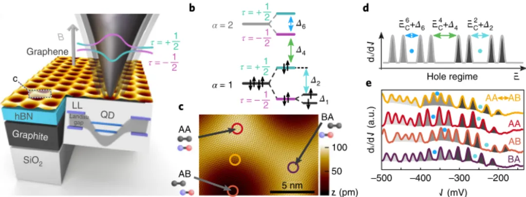
We have recently demonstrated smoothly confined Dirac fermi- ons in an edge-free graphene quantum dot (QD) by combining the electric field of the tip with a perpendicular magnetic field (Fig. 1a)22. This field quantizes the continuous spectrum of graphene in terms of Landau levels (LLs, LL spacing ≈ 100 meV at B = 7 T)18. The elec- tric field of the tip exploits the energy gaps between LLs to achieve edge-free confinement, that is, it shifts energy levels from the LLs into the gap22. We thereby overcome the well-known problem of edge localization within etched graphene QDs23. By confining with- out resorting to physical edges, these dots preserve the two-fold val- ley and spin symmetries of pristine graphene (Fig. 1b,d).
Charging of the confined levels has been directly measured by tuning the voltage of the scanning tunnelling miscroscope (STM) tip
such that the states cross the Fermi level EF. This revealed the most regularly spaced charging sequence of graphene QDs achieved so far22. The measured level separations have been reproduced with the help of tight binding (TB) calculations. Hence, the charging peaks could be assigned to LLs and to particular orbital and valley states.
Most notably, we observe quadruplets of charging peaks belonging to a single orbital quantum number of the dot and a partial splitting of single quadruplets into two doublets, indicating the lifting of the valley degeneracy (Fig. 1b,d,e). This identification of the multiplet character goes far beyond the results achieved by chemical etching of monolayer graphene QDs23 or double-sided gating of bilayer gra- phene QDs24–26.
Movable quantum dot
Here, we explore the nanoscale variation of the charging sequence in detail. We use a heterostructure comprising a SiO2/graphite support, a hexagonal boron nitride (hBN) substrate and an active graphene layer on top, which is assembled by the dry stacking method27,28 (Fig. 1a). The atomic lattices of graphene and hBN are collinearly aligned to create a hexagonal superlattice with lat- tice constant a = 13.8 nm originating from the lattice mismatch of graphene and hBN (ref. 20). Different stacking regions of the C atoms with respect to the B and N atoms (Fig. 1c) naturally lead to a spatially varying adhesion energy as well as to a spatially varying sublattice symmetry breaking of graphene due to the inequivalent binding sites. The resulting structure has been extensively discussed in the literature29–34. It is known that the most attractive interac- tion is in the AB areas (Fig. 1c) leading to stretched central regions of graphene with AB stacking and the closest contact to the hBN.
These areas are surrounded by compressed graphene ridges of different stacking with larger separation from the hBN (refs 20,30).
However, firm conclusions on the details of the superstructure are difficult to draw, because of the lack of knowledge of the specifics of the van der Waals interaction35.
Large tunable valley splitting in edge-free graphene quantum dots on boron nitride
Nils M. Freitag
1, Tobias Reisch
2, Larisa A. Chizhova
2, Péter Nemes-Incze
1,3, Christian Holl
1, Colin R. Woods
4, Roman V. Gorbachev
4, Yang Cao
4, Andre K. Geim
4, Kostya S. Novoselov
4, Joachim Burgdörfer
2, Florian Libisch
2and Markus Morgenstern
1*
Coherent manipulation of the binary degrees of freedom is at the heart of modern quantum technologies. Graphene offers two binary degrees: the electron spin and the valley. Efficient spin control has been demonstrated in many solid-state systems, whereas exploitation of the valley has only recently been started, albeit without control at the single-electron level. Here, we show that van der Waals stacking of graphene onto hexagonal boron nitride offers a natural platform for valley control. We use a graphene quantum dot induced by the tip of a scanning tunnelling microscope and demonstrate valley splitting that is tun- able from − 5 to + 10 meV (including valley inversion) by sub-10-nm displacements of the quantum dot position. This boosts the range of controlled valley splitting by about one order of magnitude. The tunable inversion of spin and valley states should enable coherent superposition of these degrees of freedom as a first step towards graphene-based qubits.
NATuRe NANoTeCHNoLoGY | VOL 13 | MAY 2018 | 392–397 | www.nature.com/naturenanotechnology 392
The tip-induced graphene QD can be moved across the graphene superstructure by moving the STM tip37. This allows us to tune the QD properties, which we probe by tracking the position of the charging peaks within the superlattice. We therefore employ spa- tially resolved dI/dV spectra (where I is the tunnelling current and V is the tip voltage). The resulting maps of charging energies can be directly compared with the corresponding topographic maps, which were recorded simultaneously (Fig. 2a). The charging peaks are fitted by Gaussians (Fig. 2b) for each QD centre position →r , ren- dering maps of the local variation of the voltage VPn( )→r of the nth peak, Pn (Fig. 2c,d). Typical variations between the centre and the boundary of the hexagonal supercell are Δ ≈VPn 40 mv. To relate this to an energy variation Δ En of a particular QD level, we employ a capacitive model yielding Δ = ΔEn e Vη Pn with the lever arm η ≃ .0 5 (Supplementary Section 4) and electron charge e. The Δ En varia- tions are primarily caused by the spatially varying adhesion energy across the supercell, which varies on the 10 meV scale according to extensive model calculations30. Figure 2c and d also show a long- range variation on the 50 nm scale (amplitude Δ ≃VPn 40 mV), which we attribute to the uncontrolled, long-range disorder potential of graphene on hBN with a strength of about 20 meV and correlation length of about 50 nm. Similar disorder potentials have been found previously38,39. Note that we carefully avoid tip forces lifting the gra- phene layer by regularly recording I(z) curves (z is the tip–sample distance) to verify that the current remains below the threshold where a slope change of ln(I(z)) indicates lifting40,41.
Tracking orbital, valley and spin splitting
The group of the first four charging peaks, P1 to P4, is associated with the quadruplet belonging to the first hole orbital of the QD. During the charging of these levels, the QD exhibits a depth of about 100 meV and a width of about 50 mn, as known from detailed Poisson calcu- lations22 (Supplementary Section 3 and 4). The confined wavefunc- tions are labeled ψα,τ,σ with orbital quantum number α = 1 for the first
four peaks, valley quantum number τ = ±12 and spin quantum num- ber σ = ±21. Analogously, the next four peaks, P5 to P8, belong to the filling of the quadruplet ψα=2,τ,σ. Subtracting the voltage of the high- est peak of the first quadruplet VP4 (Fig. 2c) from that of the lowest peak of the second, VP5 (Fig. 2d), and multiplying by η, yields the locally varying addition energy map Eadd4 ( )→ = ∣ → − → ∣r e Vη P5( )r VP4( )r (Fig. 2e). It consists of the charging energy EC4( )→r and the energy
difference → − →
− − + +
E2, ,12 12( )r E1, ,12 12( )r . The latter includes the val-
ley splitting → − →
α+ σ α− σ
E , ,12 ( )r E , ,12 ( )r and the considerably smaller Zeeman splitting Eα τ, ,+12( )→ −r Eα τ, ,−12( )→ =r g BμB ≈ .0 8 meV (where g = 2 is the gyromagnetic factor of graphene and μB is the Bohr magneton). The dominant contribution comes from the orbital
splitting → − →
τ σ τ σ
E2, , ( )r E1, , ( )r , as known from TB calculations22. As the size of the wave function does not change greatly as a function of →r (see Supplementary Video), the spatial variation of EC4( )→r cannot explain the strong spatial variation of Eadd4 ( )→r , which varies by a factor of two. Hence, Eadd4 ( )→r (Fig. 2e) mostly maps out the orbital-energy spacing between α = 1 and α = 2, as the quantum dot is moved across the graphene superstructure. Periodic depressions in the centre of the supercell reveal the influence of the superstructure on the orbital splitting, while the long-range struc- ture in Fig. 2e (50 nm scale) is again attributed to the long-range potential disorder.
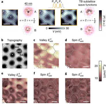
For clarity, we focus now on the second hole orbital shell α = 2 (Fig. 3); other Eaddn maps are provided in Supplementary Sections 6 and 7. The local variation of the voltage peaks belonging to the α = 2 quadruplet allows the valley and spin splittings to be mapped in detail. The voltage maps, VP6 and VP7, differ on length scales well below that of the supercell size (~10 nm), and much smaller than the size of the QD wave function (diameter ≈ 40 nm, calcu- lated by our TB approach) (Fig. 3a). The addition energy maps (Fig. 3e–g) clearly display short-range supercell-periodic variations on the length scale of 3 nm. These variations appear as dark, ring-like structures around the AB stacking region of the supercell in the
B
d a
V(mV) V
b
c
dI/dIIV
E
–300 –500 –400
e
AA AB BA AA AB
dI/dIIV (a.u.)V
Δ6
Δ4
Δ1
Δ2 Hole regime
E444C
E E+Δ4
E666C
E
E+Δ6 EEEC222+Δ2
c
α = 2
α== 1
5 nm AA
Graphene
LL QD
Landau
hBN gap
SiO2 Graphite
AB
BA BA
0 50 00 10
z ((pm) z τ = +1
2
τ = + 12
τ = – 12
τ = – 12 τ = + 12 τ = – 12
Fig. 1 | edge-free quantum dot. a, Sketch of the experiment. Coloured blocks on the left show the stacking sequence SiO2/graphite/hBN/graphene22. The STM tip (grey cone) is moved over graphene deposited on hBN with its honeycomb lattice collinearly aligned with that of the hBN (brown–yellow STM image with hBN-induced superstructure, V = 300 mV, I = 1 nA). A perpendicular B field (7 T, grey arrow) leads to Landau levels (LL, purple lines) and corresponding Landau gaps (grey area). The electric field of the tip induces band bending (curvature of Landau gap), leading to confined states (blue lines), and hence to a QD. The QD is moved by moving the STM tip above the superstructure (light grey areas around the cone). This modifies the confined state energies as the valley levels τ = 1/2 and τ = − 1/2 associated with the K and K′ points of the unperturbed band structure (cyan and magenta lines). The rectangle marked c indicates the magnified area shown in c. b, Schematic energy level diagram of the QD. The two orbital levels α = 1 and α = 2 exhibit valley splitting Eα τ,=+ ∕1 2,σ−Eα τ,=− ∕1 2,σ. The Zeeman splitting Eα τ σ, ,=+ ∕1 2−Eα τ σ, ,=− ∕1 2 is small (approximately 800 μ eV) and only shown for the lowest valley state. The resulting energy distances Δn between adjacent levels are labelled with consecutive n. Δn for odd n correspond to Zeeman splittings, which is only displayed for n = 1. c, Atomically resolved STM image of the rectangular area marked in a (V = 137 mV, I = 0.3 nA). Different stacking areas (AA, AB, BA) are indicated by arrows with stick and ball models below the labels (C, grey; B, blue; N, red). Coloured rings mark the positions of the spectra in e. d, Sketch of the expected dI/dV peak sequence for hole charging according to the level diagram in b using the same coloured arrows and the same Δn; ECn is the charging energy for filling of the nth level. Blue dots highlight valley gaps. e, dI/dV spectra recorded at the positions encircled by the same colour in c with corresponding stackings marked (AA↔ AB: between AA and AB). Quadruplets of charging peaks that belong to the same orbital are shaded the same. Blue dots mark valley transitions. Predominant quadruplet sequences (yellow spectrum), predominant doublet sequences (purple spectrum), or a mixture of both (red and orange spectra) appear, Vstab = 1 V, Istab = 700 pA, root-mean-square value Vmod = 4.2 mV, B = 7 T, temperature T = 8 K.
valley addition energy map Eadd6 . Similar but slightly narrower rings appear in the spin addition energy maps Eadd5 and Eadd7 .
Analysing the valley splitting maps
We analyse these remarkably strong nanometer-scale variations by performing TB calculations31,42. The calculations feature three major ingredients: (1) the sublattice-independent local on-site potential → V0( )r , which represents the spatially varying adhesion energy; (2) the
sublattice symmetry-breaking on-site potential Vz( )→r caused by the spatially varying stacking; and (3) a locally varying hopping ampli- tude Y( ) accounting for strain that also breaks sublattice symme-→r try18,34,41. We use an average distance between graphene and hBN of 3.3 Å, originating from density functional theory (DFT) calculations that employ the random phase approximation29. This distance is consistent with cross-sectional electron microscopy data43. To obtain locally varying TB parameters, we first employ a continuum model of graphene with known elastic constants32 subject to the potential landscape from the hBN (ref. 30). This reproduces the corrugation of 70 pm and the strain variation of 2% that are visible in the STM data (Fig. 2a)20. Based on the resulting membrane shape of the graphene layer, a molecular dynamics simulation using isotropic Lenard–
Jones potentials is employed to obtain the atomically resolved strain, the variations in the local distance between hBN and graphene, and the local stacking configuration (Supplementary Section 9).
Using these input parameters, we determine V0( )→r , Vz( )→r and Y( ) →r from our own DFT calculations (Supplementary Section 10). The potentials and hopping parameters provide, in turn, the input to our third-nearest neighbour TB calculation of the QD states22,31,42. We emphasize that no freely adjustable parameter enters our simulation.
More details are described in Supplementary Sections 9–11.
In agreement with the experiment, the calculated energies of the two valley states of the second orbital feature a pronounced varia- tion with QD position (Fig. 4a–d). To disentangle the influences of the strain and the interaction with the hBN substrate, we analyse the contributions due to V0( )→r , Vz( )→r , and Y( ) separately. Although V→r 0
(Fig. 4a) introduces local variations in the energy of the hole orbital α = 2 along the path AA↔ AB↔ BA, it does not lift the fourfold val- ley and spin degeneracy. Vz( )→r , by contrast, lifts the degeneracy between the two valley states Ψ2, ,+12σ and Ψ2, ,−12σ and even leads to an inversion of the energetic order in the AA region of the superlat- tice, that is, a change of sign for E2, ,+12σ−E2, ,−12σ (Fig. 4b). However, only when the contribution of strain is accounted for through Y( ), →r which inverts the sign of the valley splitting in the BA region (Fig. 4c), does the correct overall level ordering with level inversion in the AB region, as seen in our experiment, emerge (Fig. 4d).
The addition energies in both the TB model (Fig. 4e) and the experiment (Fig. 4f), show the same variation of about 6 meV and the same order of maxima and minima along the displacement
P4
–290 –330
dI/dV
V (mV)
V (mV) V (mV)
–250 –350
Gaussian fits
Topography
Eadd (meV) 4
10 20 Create addition energy maps
–260 –300 –280
Eadd4
0 103
z (pm)
a b
c d
e
20 nm
P5
20 nm 20 nm
20 nm
P5 P4
Fig. 2 | Addition energy maps from dI/dV spectra. a, STM image of graphene collinearly aligned to the hBN substrate (V = 400 mV, I = 300 pA, B = 7 T, T = 8 K). The overlay of grey lines marks the supercell boundary deduced from the topography. b, Sketched charging peak sequence with highlighted peaks P4 and P5 separated by addition energy Eadd4 (top) and a typical dI/dV curve (yellow line) with Gaussian fits (dashed lines) used to determine peak voltages VPn (bottom). c,d, Maps of VP4 (c) and
VP5 (d) of the area shown in a with identical grey lines overlaid, and the same parameters for measurement of the map of dI/dV curves as in Fig. 1e. The slight shift of the observed patterns with respect to the grey lines is attributed to a small lateral shift (∼ 2 nm) of the tunnelling atom with respect to the centre of the QD36. e, Eadd4 map deduced by
→ = η∣ → − →∣
Eadd4 ( )rr e VP5( )rr VP4( )rr , with the same grey lines overlaid as in a,c,d.
AB BA BA AA AA
*
α= 2 2τ= ++ 1122 αα= 2 = 2τ= = – 12
Topography
P5P6P7
*
P5 P6 P7
0 30
A A
B
B BB
A A TB sublattice wave functionsave functions
∣Ψ∣(a.u.)
ValleyEEEadd2
Valley EEEadd6
Spin EEEadd3
Spin EEEadd5 Spin EEEadd7 40 nm
a
b c d
e f g
V (mV) V
EEaddEE(meV) (meV)
100 200
Fig. 3 | Addition energy maps for spin and valley gaps. a, VPn( )→rr displayed at identical contrast for n = 5, 6, 7. The corresponding charging sequence is sketched on top. The diagonal stripes are caused by the atomic lattice of graphene via a moiré effect as outlined in Supplementary Section 8. The asterisk in P5 marks the identical position in b. Also shown are the moduli of the wavefunctions for the second hole orbital, ∣Ψα=2,τ=+ ∕1 2∣ and
Ψα= τ=− ∕
∣ 2, 1 2∣, decomposed into the two sublattice contributions, marked by A and B, calculated by our TB model. The centre of the quantum dot is in the AB stacking region. Grey honeycombs on top of the wavefunctions mark the unit cells of the graphene superstructure. Note the different length scales of
∣ ∣Ψ maps and VPn maps. b, STM image of graphene on hBN including the area shown in a. Grey lines mark supercell boundaries. Different stacking areas (AA, AB, BA) are indicated (V = 400 mV, I = 300 pA). c–g, Eaddn ( )→rr maps exhibiting identical contrast and belonging to valley and spin gaps as indicated. The same grey lines as in b are overlaid. Scale bars in a–g, 10 nm.
The same parameters are used as for the dI/dV spectra in Fig. 1e.
NATuRe NANoTeCHNoLoGY | VOL 13 | MAY 2018 | 392–397 | www.nature.com/naturenanotechnology 394
coordinate x. Hence, we attribute the periodically appearing rings that encircle the AB region (Fig. 3e), which correspond to the bump at X0 with adjacent minima in Fig. 4e, as the positions of an inver- sion of valley ordering. Remaining quantitative differences between the TB model and experiment (Fig. 4e,f) are attributed to disorder, most likely to be due to residual irregular strains caused by the non- perfect collinear alignment between graphene and hBN. The result- ing disorder is directly visible as irregularities in the unit cell of the superstructure (Figs. 2a and 3b) and also explains the irregular dis- tortions of the rings around the AB regions.
The assignment of the rings around the AB region to valley inversions is corroborated by the appearance of the small bump in the ring minimum, marked X0 in Fig. 4e–h. It is found in theory and experiment with a height of less than 1 meV. The theoretical level diagram (Fig. 4g) provides a simple explanation: the bump is the result of the additional spin splitting during the passage through the crossing of valley levels. At X0, Eadd6 consists of EC6 and the spin splitting E2, ,τ12−E2, ,τ −12 ≈800 μ eV reduced by anticrossing contri- butions. In contrast, the two spatially offset crossings of valley states with different spins (blue circles in Fig. 4g) feature only EC6, resulting in the minima around the bump. Figure 4g also explains the rings in the spin splitting maps (Fig. 3f,g), which are simply the reduced Δ5 and Δ7 at X0. The spatial alignment of the bump in Δ6 and the minima in Δ5,7 are nicely corroborated by the experiment (Fig. 4h).
Although we have focused here on the valley splitting of the sec- ond hole state, similar ring-like structures encircling the AB area are also found for the third hole orbital α = 3 with tunability of the valley crossing up to 15 meV (Supplementary Fig. 2). In contrast, the first hole orbital α = 1 (Fig. 3c,d) exhibits a valley tunability of about 7 meV without inversion of the valley ordering. On the elec- tron side, the additional charging of defects within the hBN (ref. 44) complicates the analysis45, but some ring-like structures indicat- ing valley inversion can also be spotted (Supplementary Section 6).
Data recorded with another microtip at two different B fields exhibit very similar features (Supplementary Fig. 3). Moreover, the energy range of valley tunability remains independent of B, providing sup- port for the valley tuning being caused by the interaction with the substrate and not by the B field. For example, the strength of the exchange enhancement would vary with B. In addition, it turns out to be one order of magnitude too weak to explain the experimen- tally observed valley tuning (Supplementary Section 14).
A simple estimate clarifies the resulting strength of the val- ley splitting of about 10 meV. The sublattice breaking interac- tions themselves (Vz( )→r , Y( )) spatially vary by about 100 meV as →r deduced from our DFT calculations (Supplementary Section 10).
Hence, shifting about 10% of the hole density of a state (∝∣ ∣Ψ 2) from the unfavourable AB to the favourable AA region is sufficient to account for variations of the valley splitting of about 10 meV.
Indeed, our detailed TB calculations find that the α = 2 wave func- tion covers about ten unit cells (Fig. 3a) and primarily adjusts its distribution within the central unit cell due to the changing poten- tial landscape (see Supplementary Video).
Conclusions and outlook
The revealed tunability of a valley splitting by up to 15 meV sur- passes the highest reported values of valley tuning for other poten- tially nuclear-spin-free host materials (Si/SiO2, 500 μ eV) by more than one order of magnitude. Hence, it might be exploited at temperatures up to 4 K. Most intriguingly, the crossings of valley and spin levels depicted in Fig. 4g can be used to initialize superposition states of spin and valley degrees of freedom2,46. This could be the starting point to determine the coherence47 of both types of states in graphene for the first time. The required interaction of the levels rendering the depicted crossings into anticrossings is naturally provided by the spatially vary- ing sublattice potential that couples opposite valley states (Fig. 4d).
We note in passing that the breaking of the valley degeneracy is also
e g Valley anticrossings at XXX0
10 16 14 12
0
–8 –4 4 8
x (nm) x
0
–8 –4 4 8
x (nm) x
AA AB BA
X X00 X X Calculation
Experiment
Valleypolarization
4 10
12 14
X (nm) X
n = 6 n = 5 n n = 7 n
f h
a
b
0 5
–5
V0 V V
εjε (meV)j
0 5 –5
Vz V V
0 5 –5
Strain
c
0 5 –5
V0 V
V + VVVz + straini
Δ6
d
10 16 14 12 XXXXXX00
X0 X X
x –10
– –5 5 10
–55 5 10
–10
x (nm) x
x (nm) x x x
AA AB BA
τ = + 2
τ = – 2
EaddEE (meV)6EaddEE (meV)6 εjε EaddEE (meV)n
–4 τ = –2 τ = +2
τ = +2
τ = –2
1
1
ΔΔ77
ΔΔ5
Δ6
1 1
1
1
X X0 X X
Fig. 4 | Valley crossing. a–d, TB energies (εj) of the two valley states of the second QD hole orbital (α = 2) as a function of the centre position of the QD.
Different stackings at this centre along a high-symmetry line of the superstructure are labelled at the top. The valley polarization is colour coded (see scalebar). a, TB energies, if only the sublattice-independent potential V0( )→rr is considered. b, TB energies, if only the sublattice symmetry-breaking on-site potential Vz( )→rr is considered. c, TB energies, if only the varying hopping parameter Y( ) due to strain is considered. d, The sum of all three contributions. →rr The valley splitting Δ6 determining the spatial variation in e is indicated by a double arrow in d, B = 7 T. e, Theoretical prediction for Eadd6 based on d (Supplementary Section 10). f, Experimental addition energy Eadd6 along the corresponding arrow in the inset (same Eadd6 ( )→rr map as Fig. 3d). The x axis is aligned to the stackings marked in e. X0 indicates a feature attributed to the influence of spin splitting at the valley crossing. The origin in a–f is the centre of the AB region. g, Schematic evolution of the state energies for a crossing of two valley states (τ = + 1/2: cyan, τ = − 1/2: magenta). A spatially constant spin splitting (levels marked by black spin arrows) is added. The resulting energy differences Δn are marked by double arrows. An anticrossing emerges at X0 as deduced from d. Blue circles mark spin level crossings. h, Experimental Eaddn ( )→rr along the red line in the inset of f, belonging to one preferential valley gap (red) and two spin gaps (grey). A typical error bar, resulting from the Gaussian fits of the dI/dV peaks, is shown.
the central requirement for exchange-based spin qubits, which could provide an all-electrical spin qubit operation in graphene48. A possible device set-up for these purposes could employ side gates for moving gate-based QDs and, hence, for providing the valley tuning. Edge states, belonging to each LL, can provide tunable source and drain contacts (Supplementary Section 15).
Finally, we emphasize that the approach of designed van der Waals heterostructures19–21 for a versatile tuning of electronic degrees of freedom might be extended to physical spin schemes by using an atomically varying spin–orbit interaction as present for graphene on WSe249, for example.
Methods
Methods, including statements of data availability and any asso- ciated accession codes and references, are available at https://doi.
org/10.1038/s41565-018-0080-8.
Received: 28 August 2017; Accepted: 25 January 2018;
Published online: 19 March 2018 References
1. Ladd, T. D. et al. Quantum computers. Nature 464, 45–53 (2010).
2. Pioro-Ladriere, M. et al. Electrically driven single-electron spin resonance in a slanting Zeeman field. Nat. Phys. 4, 776–779 (2008).
3. Wu, X. et al. Two-axis control of a singlet-triplet qubit with an integrated micromagnet. Proc. Natl Acad. Sci. USA 111, 11938–11942 (2014).
4. Abanin, D. A. et al. Giant nonlocality near the Dirac point in graphene.
Science 332, 328–330 (2011).
5. Shimazaki, Y. et al. Generation and detection of pure valley current by electrically induced Berry curvature in bilayer graphene. Nat. Phys. 11, 1032–1036 (2015).
6. Sui, M. et al. Gate-tunable topological valley transport in bilayer graphene.
Nat. Phys. 11, 1027–1031 (2015).
7. Ju, L. et al. Topological valley transport at bilayer graphene domain walls.
Nature 520, 650–655 (2015).
8. Wallbank, J. R. et al. Tuning the valley and chiral quantum state of Dirac electrons in van der Waals heterostructures. Science 353, 575–579 (2016).
9. Rahman, R. et al. Engineered valley-orbit splittings in quantum-confined nanostructures in silicon. Phys. Rev. B 83, 195323 (2011).
10. Yang, C. H. et al Spin-valley lifetimes in a silicon quantum dot with tunable valley splitting. Nat. Commun. 4, 2069 (2013).
11. Gokmen, T. et al. Parallel magnetic-field tuning of valley splitting in AlAs two-dimensional electrons. Phys. Rev. B 78, 233306 (2008).
12. Kobayashi, T. et al. Resonant tunneling spectroscopy of valley eigenstates on a donor-quantum dot coupled system. Appl. Phys. Lett. 108, 152102 (2016).
13. Gamble, J. K. et al. Valley splitting of single-electron Si MOS quantum dots.
Appl. Phys. Lett. 109, 253101 (2016).
15. Mi, X., Péterfalvi, C. G., Burkard, G. & Petta, J. High-resolution valley spectroscopy of Si quantum dots. Phys. Rev. Lett. 119, 176803 (2017).
16. Xiao, D., Yao, W. & Niu, Q. Valley-contrasting physics in graphene:
Magnetic moment and topological transport. Phys. Rev. Lett. 99, 236809 (2007).
17. Pesin, D. & MacDonald, A. H. Spintronics and pseudospintronics in graphene and topological insulators. Nat. Mater. 11, 409–416 (2012).
18. Castro Neto, A. H., Guinea, F., Peres, N. M. R., Novoselov, K. S. &
Geim, A. K. The electronic properties of graphene. Rev. Mod. Phys. 81, 109–162 (2009).
19. Geim, A. K. & Grigorieva, I. V. Van der Waals heterostructures. Nature 499, 419–425 (2013).
20. Woods, C. R. et al. Commensurate-incommensurate transition in graphene on hexagonal boron nitride. Nat. Phys. 10, 451–456 (2014).
21. Novoselov, K. S., Mishchenko, A., Carvalho, A. & Castro Neto, A. H.
2D materials and van der Waals heterostructures. Science 353, 461–470 (2016).
22. Freitag, N. M. et al. Electrostatically confined monolayer graphene quantum dots with orbital and valley splittings. Nano Lett. 16, 5798–5805 (2016).
23. Bischoff, D. et al. Localized charge carriers in graphene nanodevices.
Appl. Phys. Rev. 2, 031301 (2015).
24. Allen, M. T., Martin, J. & Yacoby, A. Gate-defined quantum confinement in suspended bilayer graphene. Nat. Commun. 3, 934 (2012).
25. Goossens, A. M. et al. Gate-defined confinement in bilayer graphene- hexagonal boron nitride hybrid devices. Nano Lett. 12, 4656–4660 (2012).
26. Müller, A. et al. Bilayer graphene quantum dot defined by topgates.
J. Appl. Phys. 115, 233710 (2014).
27. Mayorov, A. S. et al. Micrometer-scale ballistic transport in encapsulated graphene at room temperature. Nano Lett. 11, 2396–2399 (2011).
28. Kretinin, A. V. et al. Electronic properties of graphene encapsulated with different two-dimensional atomic crystals. Nano Lett. 14, 3270–3276 (2014).
29. Sachs, B., Wehling, T. O., Katsnelson, M. I. & Lichtenstein, A. I. Adhesion and electronic structure of graphene on hexagonal boron nitride substrates.
Phys. Rev. B 84, 195414 (2011).
30. van Wijk, M. M., Schuring, A., Katsnelson, M. I. & Fasolino, A. Moiré patterns as a probe of interplanar interactions for graphene on h-BN. Phys.
Rev. Lett. 113, 135504 (2014).
31. Chizhova, L. A., Libisch, F. & Burgdörfer, J. Graphene quantum dot on boron nitride: Dirac cone replica and Hofstadter butterfly. Phys. Rev. B 90, 165404 (2014).
32. San-Jose, P., Gutiérrez-Rubio, A., Sturla, M. & Guinea, F. Spontaneous strains and gap in graphene on boron nitride. Phys. Rev. B 90, 075428 (2014).
33. Slotman, G. J. et al. Effect of structural relaxation on the electronic structure of graphene on hexagonal boron nitride. Phys. Rev. Lett. 115, 186801 (2015).
34. Jung, J. et al. Moiré band model and band gaps of graphene on hexagonal boron nitride. Phys. Rev. B 96, 085442 (2017).
35. Ambrosetti, A., Ferri, N., DiStasio, R. A. Jr. & Tkatchenko, A. Wavelike charge density fluctuations and van der Waals interactions at the nanoscale.
Science 351, 1171–1176 (2016).
36. Morgenstern, M. et al. Origin of Landau oscillations observed in scanning tunneling spectroscopy on n-InAs(110). Phys. Rev. B 62, 7257–7263 (2000).
37. Dombrowski, R., Steinebach, C., Wittneven, C., Morgenstern, M. &
Wiesendanger, R. Tip-induced band bending by scanning tunneling spectroscopy of the states of the tip-induced quantum dot on inas(110).
Phys. Rev. B 59, 8043–8048 (1999).
38. Xue, J. M. et al. Scanning tunnelling microscopy and spectroscopy of ultra-flat graphene on hexagonal boron nitride. Nat. Mater. 10, 282–285 (2011).
39. Decker, R. et al. Local electronic properties of graphene on a BN substrate via scanning tunneling microscopy. Nano Lett. 11, 2291–2295 (2011).
40. Mashoff, T. et al. Bistability and oscillatory motion of natural
nanomembranes appearing within monolayer graphene on silicon dioxide.
Nano Lett. 10, 461–465 (2010).
41. Georgi, A. et al. Tuning the pseudospin polarization of graphene by a pseudomagnetic field. Nano Lett. 17, 2240–2245 (2017).
42. Libisch, F., Rotter, S., Güttinger, J., Stampfer, C. & Burgdörfer, J. Transition to Landau levels in graphene quantum dots. Phys. Rev. B 81,
245411 (2010).
43. Haigh, S. J. et al. Cross-sectional imaging of individual layers and buried interfaces of graphene-based heterostructures and superlattices. Nat. Mater.
11, 764–767 (2012).
44. Wong, D. et al. Characterization and manipulation of individual defects in insulating hexagonal boron nitride using scanning tunnelling microscopy.
Nat. Nanotech. 10, 949–953 (2015).
45. Morgenstern, M., Freitag, N., Nent, A., Nemes-Incze, P. & Liebmann, M.
Graphene quantum dots probed by scanning tunneling microscopy.
Ann. Phys. 529, 1700018 (2017).
46. Petta, J. et al. Coherent manipulation of coupled electron spins in semiconductor quantum dots. Science 309, 2180–2184 (2005).
47. Elzerman, J. M. et al. Single-shot read-out of an individual electron spin in a quantum dot. Nature 430, 431–435 (2004).
48. Trauzettel, B., Bulaev, D. V., Loss, D. & Burkard, G. Spin qubits in graphene quantum dots. Nat. Phys. 3, 192–196 (2007).
49. Wang, Z. et al. Origin and magnitude of ‘designer’ spin-orbit interaction in graphene on semiconducting transition metal dichalcogenides. Phys. Rev. X 6, 041020 (2016).
Acknowledgements
The authors appreciate helpful discussions with C. Stampfer, H. Bluhm, R. Bindel, M. Liebmann and K. Flöhr as well assistance during the measurements by A. Georgi.
N.M.F., P.N.-I. and M.M. acknowledge support from the European Union Seventh Framework Programme under Grant Agreement no. 696656 (Graphene Flagship) and the German Science foundation (Li 1050-2/2 through SPP-1459), L.A.C., J.B. and F.L. from the Austrian Fonds zur Förderung der wissenschaftlichen Forschung (FWF) through the SFB 041-ViCom and doctoral college Solids4Fun (W1243). TB calculations were performed on the Vienna Scientific Cluster. R.V.G., A.K.G. and K.S.N. also acknowledge support from the EPSRC (Towards Engineering Grand Challenges and Fellowship programs), the Royal Society, the US Army Research Office, the US Navy Research Office and the US Airforce Research Office. K.S.N. is also grateful to the ERC for support via Synergy grant Hetero2D.
A.K.G. was supported by Lloyd's Register Foundation. P.N.-I. acknowledges support from the Hungarian Academy of Sciences Lendület under grant no. LP2017-9/2017.
NATuRe NANoTeCHNoLoGY | VOL 13 | MAY 2018 | 392–397 | www.nature.com/naturenanotechnology 396
Author contributions
N.M.F. carried out the STM measurements with assistance of P.N.-I. and C.H. and evaluated the experimental data under supervision of P.N.-I. and M.M. P.N.-I. performed the strain calculations, while T.R., F.L., and L.A.C. contributed DFT and TB calculations.
C.R.W., Y.C., R.V.G., A.K.G. and K.S.N. provided the sample. M.M. conceived and coordinated the project together with N.M.F., P.N.-I. and F.L. The comparison between theory and experiment was conducted by N.M.F., M.M., F.L. and P.N.-I. M.M., N.M.F., P.N.-I. and F.L. wrote the manuscript with contributions from all authors.
Additional information
Supplementary information is available for this paper at https://doi.org/10.1038/
s41565-018-0080-8.
Reprints and permissions information is available at www.nature.com/reprints.
Correspondence and requests for materials should be addressed to M.M.
Publisher’s note: Springer Nature remains neutral with regard to jurisdictional claims in published maps and institutional affiliations.
Methods
The sample was prepared by exfoliating graphite flakes on a SiO2 substrate, followed by two consecutive dry transfers27,28 of 30-nm-thick hexagonal hBN and monolayer graphene, respectively. During the graphene transfer, we took care to minimize the angular misalignment between the graphene lattice and the hBN lattice. Remaining small misalignments in the 0.1° regime cannot be excluded20. Moreover, a few small bubbles between the graphene and the hBN appear after transfer (see chapter S7 of ref. 41). Both of these effects lead to mechanical stresses that perturb the graphene/hBN superlattice in period or shape50 (Figs. 2a and 3b).
The graphene flake overlaps the hBN completely. This avoids insulating areas, which would be hazardous to the STM tip, but does not allow for back-gate operation. Finally, electrical Cr/Au contacts (2 nm/100 nm) are evaporated onto the large bottom graphite flake via a shadow mask. Optical images of the device structure are available in the supplement of a previous publication22.
STM and scanning tunnelling spectroscopy measurements are performed in a home-built ultrahigh vacuum STM chamber operating at temperature T = 8 K and in magnetic fields up to B = 7 T perpendicular to the surface51. Tungsten tips are prepared by etching W wires, which are subsequently controlled with an optical microscope. The microtips are transferred into the STM within the ultrahigh vacuum chamber, where they are reshaped by controlled indentation into the Au(111) surface of a Au bead52. They thus form a Au apex of a few tens of nanometres in length as cross-checked by electron microscopy. We characterize the tips in situ by mapping the topographic and spectroscopic features of the Au(111) surface before exchanging the Au crystal for the graphene sample. STM images are recorded in constant current mode at tunnelling current I and tip voltage V.
Differential conductance curves dI/dV(V) are recorded by lock-in detection using a modulation voltage with root-mean-square value Vmod= 2–5 mV and frequency fmod = 1,223 Hz. After stabilizing the tip–sample distance at stabilization voltage Vstab and stabilization current Istab, the feedback loop is opened for the dI/dV(V)
recording. During the recording, the tip–sample distance is changed at a rate of 50 pm V−1, approaching the sample by 0.5 Å while sweeping V from 1 V to 0 V and retracting it by the same distance while continuing to − 1 V. This compensates for the changing height of the tunnelling barrier as a function of V (ref. 53). The resulting change in the tip–sample capacitance is below 2.5%22. It is therefore neglected, as it is much smaller than other capacitance uncertainties22. Additionally, we normalize the dI/dV data according to dI/dV(V))/I(Vstab) with I(Vstab) being the first detected current after opening the feedback loop. This compensates for the influence of vibrations during the stabilization process.
We focus on the first two orbital states for confined holes, originating from LL−1, as they capture the essential features (see Supplementary Section 6). On the electron side, charging of randomly distributed defects in the hBN (ref. 44) impedes an unambiguous analysis of the QD charging patterns (see Supplementary Fig. 2)45. Data availability. The data that support the plots within this paper and other findings of this study are available from the corresponding author upon reasonable request.
References
14. Scarlino, P. et al. Dressed photon-orbital states in a quantum dot: Intervalley spin resonance. Phys. Rev. B 95, 165429 (2017).
50. Jiang, Y. et al. Visualizing strain-induced pseudomagnetic fields in graphene through an hBN magnifying glass. Nano Lett. 17, 2839–2843 (2017).
51. Mashoff, T., Pratzer, M. & Morgenstern, M. A low-temperature high resolution scanning tunneling microscope with a three-dimensional magnetic vector field operating in ultrahigh vacuum. Rev. Sci. Instr. 80, 053702 (2009).
52. Voigtländer, B., Cherepanov, V., Elsaesser, C. & Linke, U. Metal bead crystals for easy heating by direct current. Rev. Sci. Instr. 79, 033911 (2008).
53. Feenstra, R. Tunneling spectroscopy of the (110)-surface of direct-gap III-V semiconductors. Phys. Rev. B 50, 4561–4570 (1994).
NATuRe NANoTeCHNoLoGY | www.nature.com/naturenanotechnology