Memory Access Optimization for Computations on Unstructured Meshes
Thesis submitted for the degree of Doctor of Philosophy
Antal Hiba M.Sc.
Supervisors:
Dr. P´ eter Szolgay, Dr. Mikl´ os Ruszink´ o
P´ azm´ any P´ eter Catholic University
Faculty of Information Technology and Bionics Roska Tam´ as Doctoral School of Sciences and Technology
Budapest, 2015
DOI:10.15774/PPKE.ITK.2016.007
Contents
1. Introduction 1
1.1. Motivation and scope . . . 1
1.2. Thesis outline . . . 3
2. Bandwidth limitations in mesh computing 5 2.1. Processors and Memory Interfaces . . . 6
2.1.1. Comparison of different processor architectures from 2013 . . . 6
2.1.2. Processor architectures from 2015 . . . 7
2.1.3. Possible Hardware Solutions to the Memory Wall . . . 10
2.2. Mesh Computing . . . 10
2.3. Dataflow Computing . . . 12
2.3.1. Dataflow computing on a mesh . . . 12
2.3.2. Memory access optimization and interprocessor communication . . . 14
2.3.3. Data Locality in Mesh Computing . . . 15
3. Dataflow Machines 17 3.1. FPGA and All Programmable System on Chip (APSoC) architectures . . . 17
3.1.1. Field Programmable Gate Array (FPGA) . . . 17
3.1.2. All Programmable System on Chip (APSoC) . . . 20
3.2. Existing hardware solutions of DMs . . . 22
3.2.1. Maxeler accelerator architecture . . . 22
3.2.2. HC1 coprocessor board . . . 23
3.2.3. Multi-Banked Local Memory with Streaming DMA . . . 24
3.2.4. Large-Scale FPGA-based Convolutional Networks . . . 25
3.2.5. Pipelined Maxeler Accelerators . . . 26 i
ii CONTENTS
3.3. Off-chip memory streaming techniques . . . 28
3.4. Special-Purpose DMs for mesh computing . . . 31
3.4.1. DM for structured meshes . . . 31
3.4.2. DM for unstructured meshes . . . 33
3.4.3. Implementation of the DM for unstructured meshes . . . 35
4. Static Mapping 39 4.1. Graph Partitioning . . . 39
4.1.1. Bipartitioning methods . . . 40
4.1.2. Generalizations of Graph Partitioning . . . 41
4.1.2.1. Hybrid Architecture: . . . 42
4.1.2.2. Heterogeneous Processes: . . . 42
4.1.2.3. Multi-Constraint Partitioning: . . . 42
4.1.2.4. Skewed Partitioning Model: . . . 42
4.1.2.5. Target Graph Representation: . . . 42
4.2. Sparse Matrix Reordering . . . 43
4.3. Data locality and interprocessor communication . . . 43
4.3.1. Description of Graph Bandwidth Minimization and related work . . 44
4.3.2. Connection between Graph Bandwidth and Mesh Structure . . . 45
5. Bandwidth-Limited Partitioning 49 5.1. Problem definition . . . 49
5.2. AM1 partitioning method . . . 50
5.2.1. AM1 reordering method . . . 50
5.2.1.1. Two data locality bounds based on graph bandwidth . . . 51
5.2.1.2. Algorithm for bandwidth reduction . . . 51
5.2.1.3. Description of AM1 . . . 52
5.2.1.4. Results and conclusions . . . 53
5.2.2. AM1 as a partitioner . . . 54
5.2.2.1. AM1 based bounded S BW method . . . 55
5.2.2.2. Results and conclusions . . . 57
5.3. Depth-Level Structure based partitioning . . . 58
5.3.1. Depth Level Structure (DLS) Based Bisection . . . 58
DOI:10.15774/PPKE.ITK.2016.007
5.3.1.1. Objective . . . 59
5.3.1.2. Basic Entities and Operations . . . 59
5.3.1.3. DLS Bisection . . . 61
5.3.2. Results . . . 63
5.3.2.1. Bounded BW partitioning . . . 66
5.3.3. Conclusions . . . 66
5.4. BLP method for structured meshes . . . 67
5.4.1. Grid-Type BLP Partitions . . . 67
5.4.2. Quality of Grid-Type BLP partitions . . . 69
5.5. BLP method for unstructured meshes . . . 70
5.5.1. METIS-AM1 hybrid method for handling BLP . . . 71
5.5.2. METIS-AM1 results on unstructured meshes . . . 71
5.6. Conclusions . . . 73
6. Applicable Partial Solution Generation for Fast-response Combinatorial Optimization 75 6.1. Variable Subset Merger . . . 77
6.1.1. Variations of subset selection . . . 78
6.1.1.1. VSM-Const . . . 79
6.1.1.2. VSM-PLoss . . . 79
6.1.1.3. VSM-CLoss . . . 79
6.1.1.4. VSM-PCLoss . . . 80
6.1.2. VSM Hybrid Methods . . . 80
6.1.2.1. With best-known not real-time solver . . . 80
6.1.2.2. With best-known real-time solver . . . 80
6.1.3. VSM models for specific optimization problems . . . 81
6.2. VSM for the Disc Scheduling Problem (DSP) . . . 81
6.2.1. VSM model for the Disc Scheduling Problem . . . 82
6.3. VSM for the Generalized Assignment Problem . . . 83
6.3.1. Generalized Assignment Problem (GAP) . . . 83
6.3.2. VSM model for GAP . . . 83
6.4. VSM for the Sequential Ordering Problem . . . 85
6.4.1. Sequential Ordering Problem (SOP) . . . 85
6.4.2. VSM-SOP . . . 85
6.4.3. Compulsory Validations . . . 86
6.5. Results . . . 87
6.5.1. Subset selection and optimality . . . 87
6.5.2. Response time . . . 90
6.5.3. Operations with optimization time complexity . . . 91
6.6. Conclusions . . . 92
7. Theses of the Dissertation 95 7.1. Methods and tools . . . 95
7.2. New scientific results . . . 96
7.3. Applicability of the results . . . 103
References 105
iv
DOI:10.15774/PPKE.ITK.2016.007
Kivonat
A gr´afok rendk´ıv¨ul hat´ekony eszk¨oznek bizonyultak a vil´ag matematikai modellez´es´eben, kezdve a k¨oz´uti h´al´ozatokt´ol eg´eszen egy emberi ´er 3D t´erbeli le´ır´as´aig. A modellekb˝ol sz´armaz´o numerikus algoritmusok gyakran sz´am´ıt´asig´enyesek, ez´ert t¨obb processz´al´o csom´opont k¨oz¨ott fel kell oszta- ni a feladatot. A feloszt´as sor´an egy gr´af particion´al´asi feladatot kell meg- oldani. A c´el a lehet˝o leggyorsabb p´arhuzamos´ıtott sz´am´ıt´as az er˝oforr´asok maxim´alis kihaszn´al´as´aval. Az egymagos lass´u kommunik´aci´os csatorn´akkal
¨
osszek¨ot¨ott processzorok idej´eben egy´ertelm˝uen a minim´alis kommunik´aci´ot eredm´enyez˝o azonos m´eret˝u r´eszgr´afokat tartalmaz´o feloszt´asokat tekint- hett¨uk optim´alisnak. Napjaink processzor-architekt´ur´ai azonban ak´ar sok ezer m˝uveletv´egz˝o egys´eget is tartalmazhatnak, ´es kommunik´aci´os csa- torn´aik s´avsz´eless´ege csak egy nagys´agrenddel marad el a saj´at k¨ozpon- ti mem´oriael´er´es¨uk s´avsz´eless´eg´et˝ol. Kutat´asom c´elja, hogy megvizsg´aljam mely feloszt´asok optim´alisak az ´uj kiloprocesszoros architekt´ur´ak sz´am´ara, ´es term´eszetesen az ilyen feloszt´asok gener´al´as´ara m´odszereket is szeretn´ek meg- adni.
A dolgozatban bemutatom korunk legjobb processzorait, ´es ezek pa- ram´eterein kereszt¨ul a mem´oria s´avsz´eless´egkorl´at ´altal´anos probl´em´aj´at. A s´avsz´eless´egkorl´at lek¨uzd´es´enek ´altalam leghat´ekonyabbnak tal´alt ir´any´at az adatfolyam alap´u architekt´ur´akat (DM) r´eszletesen is bemutatom. Ezen spe- ci´alis processzorok FPGA-n val´os´ıthat´oak meg vagy VLSI c´elhardvarek´ent.
A DM-ek legfontosabb tulajdons´aga, hogy a processz´al´o egys´egek egy ma- xim´alis s´avsz´eless´eggel be´erkez˝o adatfolyamra csatlakoznak, a r´eszeredm´enyek ugyan´ıgy haladnak tov´abb a chip-en tov´abbi procesz´al´o elemek fel´e majd a v´egeredm´eny vissza a k¨ozponti mem´ori´aba. A DM-ek maxim´alisan kihaszn´alj´ak a mem´oria ´es a processzor k¨oz¨otti s´avsz´eless´eget, viszont az adatfolyamnak csak egy nagyon kis r´esze ´erhet˝o el egy adott id˝opillanatban (on-chip cache). Az egy
m˝uvelethez tartoz´o bemeneti adatoknak k¨ozel kell lenni¨uk egym´ashoz a soros adatfolyamban, k¨ul¨onben a m˝uvelet nem lesz elv´egezhet˝o (az egyik operandus m´eg nem ´er be, amikor a m´asikat m´ar ki kell dobni a cache-b˝ol). Az ¨osszef¨ugg˝o adatok maxim´alis t´avols´ag´at a folyamban adatlokalit´asnak nevezz¨uk.
Mivel az adatlokalit´as er˝os korl´at, sz¨uks´eges egy olyan m´odszer, amely egy adatlokalit´as korl´at teljes¨ul´es´et k´epes garant´alni a l´etrej¨ov˝o r´eszgr´afokban. Az adatlokalit´as jav´ıt´asa a m´atrix s´avsz´eless´eg minimaliz´al´as feladat´ara vezethet˝o vissza. Az irodalomban tal´alt heurisztikus m´odszerek vizsg´alata ut´an, a Gibbs- Pole-Stockmeyer (GPS) m´odszert alak´ıtottam ´at olyan particion´al´asi elj´ar´ass´a (AM1), amely adott m´atrix s´avsz´eless´eg korl´at alatt soros´ıthat´o r´eszgr´afokat hoz l´etre. Az AM1 lehet˝ov´e teszi a DM-ek alkalmaz´as´at nagyobb r´eszgr´afokra is, viszont a r´eszgr´afok sz´am´at nem lehet el˝o´ırni, ´es a l´etrej¨ov˝o r´eszgr´afok m´erete szint´en nem egys´eges´ıthet˝o. Az AM1 ¨onmag´aban csak az egy DM ´altal kezelhet˝o r´eszgr´af m´eret´et n¨oveli meg szignifik´ansan egy virtu´alis particion´al´as seg´ıts´eg´evel.
Az adatlokalit´as matematikai vizsg´alata t¨obb egyszer˝u ¨osszef¨ugg´est is eredm´enyezett az adatlokalit´as szempontj´ab´ol kedvez˝o partici´okkal kapcso- latban. Ezek alapj´an bevezettem a M´elys´egi Szint Strukt´ur´at (DLS), amely a gr´af v´egpontjaib´ol (vagy hat´arhalmazb´ol) ind´ıtott sz´eless´egi keres´es hoz l´etre. Els˝ok´ent biszekci´oval foglalkoztam, ´es a legm´elyebb szinteket sz´etv´ag´o szepar´atorokat gener´al´o m´odszert dolgoztam ki. A l´etrej¨ov˝o r´eszgr´afok adat- lokalit´as szempontb´ol j´ol viselkedtek, viszont a proceszork¨ozi kommunik´aci´o megn¨oveked´ese ´es az irregul´aris r´acsok v´altozatoss´aga miatt a m´odszer nem lett eredm´enyes.
A struktur´alt 2D ´es 3D t´eglalap vizsg´alata sor´an siker¨ult egy k¨ozel op- tim´alis m´odszert kidolgozni, amelyben az adatlokalit´as ´es a processzork¨ozi kommunik´aci´o egy¨uttesen kezelhet˝ov´e v´alt. Ez alapj´an megfogalmaztam a S´avsz´eless´eg-korl´atos Particion´al´as (BLP) feladat´at. Megvizsg´altam hogyan lehetne korunk egyik legjobb particion´al´asi m´odszer´et (METIS) a BLP fel- adat megold´as´ara felhaszn´alni. T¨obb izgalmas ¨osszef¨ugg´es mellett egy hib- rid m´odszert kaptam, amely t¨obb METIS pr´oba particion´al´as eredm´eny´eb˝ol kisz´amol egy kezdeti particion´al´ast, melynek elemeit ´atadja az AM1-nek.
vi
DOI:10.15774/PPKE.ITK.2016.007
A p´arhuzamos´ıt´ast seg´ıt˝o ´uj particion´al´asi m´odszerek mellett a dolgozat m´asodik r´esz´eben mag´anak az optimaliz´aci´onak a gyors´ıt´as´at t˝uz¨om ki c´elul.
Maga a gr´af particion´al´asi feladat is felfoghat´o egy kombinatorikus optima- liz´aci´os (CO) feladatk´ent, ahol minden csom´oponthoz tartozik egy d¨ont´esi v´altoz´o, amely meghat´arozza hogy h´anyas sorsz´am´u r´eszgr´afba ker¨ul az adott csom´opont. Az ilyen feladatok megold´as´at ´ugy k´ıv´anom gyors´ıtani, hogy egy r´eszfeladatot megoldok, ´es mik¨ozben a r´eszmegold´ast m´ar felhaszn´alom, folytatom a megmarad´o d¨ont´esi v´altoz´ok optimaliz´aci´oj´at. A m´odszertant
´
altal´anosan siker¨ult kidolgozni, ´es a Soros Rendez´esi Probl´em´an (SOP) a Lemez Utemez´¨ esi Probl´em´an (DSP) ´es az ´Altal´anos Hozz´arendel´esi Probl´em´an (GAP) be is mutatom az el˝onyeit ´es gyenge pontjait. Sajnos a BLP megold´as´anak gyors´ıt´as´ara nem aj´anlhat´o a m´odszer, viszont sok m´as esetben, ahol egy r´eszmegold´as ismerete nagyobb el˝ony¨okkel j´ar (feladatok sorbarendez´ese - SOP) jelent˝os gyors´ıt´as ´erhet˝o el.
vii
DOI:10.15774/PPKE.ITK.2016.007
Abstracts
Graphs have been found an effective tool in modeling the real world from the road network to the 3D volumetric description of a human vein. Numerical algorithms that come from these models are often computationally expensive, thus these tasks have to be divided. This division is defined by the solution of the graph partitioning problem. The partitioning aims for the best possible parallelism with maximal resource utilization. In the age of slow interconnec- tions and single-core processors, the optimal solution was clearly the one with minimal communication need and identically sized parts. However, the current processor architectures have thousands of processing elements, and the band- width of their interconnections is just one order of magnitude slower than the bandwidth of their main memory. The goal of my research is to investigate the properties of optimal partitions in the case of these novel processor architec- tures and naturally, I want to also give methods to generate these partitions.
In this work, I show the best processor architectures available today and th- rough them the general problem of memory bandwidth limitation. I present in details Dataflow Machines (DM) which provides the best solution to this problem in my view. These specific processors can be realized in FPGA or custom VLSI. The most important property of DMs is streaming, that is, the processing elements connected to a maximal bandwidth data flow and the inter- mediate results propagated the same way to other processing elements on-chip and finally the result is streamed back to the main memory. DMs utilize the whole memory bandwidth, but only a small portion of the data flow can be accessed on-chip at the same time. The operands of an operation have to be close to each other in the serialized data stream, otherwise, the operation can not be executed (one of the operands has not arrived when an other operand must be thrown out from the cache). The maximal distance of connected data elements is called data locality.
Data locality has a strict bound thus a method is required which can gua- rantee the desired locality in the resulting subgraphs. Data locality minimi- zation of a stream can be traced back to the matrix bandwidth minimization problem. After the investigation of known methods, I modified the Gibbs-Pole- Stockmeyer (GPS) method into a partitioner (AM1), which creates subgraphs with the desired data locality. AM1 makes it possible to use DMs for larger subgraphs, however, the number of subgraphs can not be defined and the size of the subgraphs can not be controlled as well. AM1 itself can increase only the size of possible inputs for DMs with a virtual partitioning.
Mathematical analysis of data locality results many simple rules about the par- titions with good data locality. Based on these observations I defined the Depth Level Structure (DLS), which is created by a Breadth-First Search started from the endpoints of the graph (or boundary elements). First, I work on bisections and I created a method which cuts the deepest areas of the graph. The resulted subgraphs have good data locality, however, the interprocesor communication need increased significantly and the variability of irregular meshes makes this approach unsuccessful.
Investigations of 2D and 3D structured rectangular meshes results a specific method which nearly optimal for these graphs, furthermore data locality and interprocessor communication can be handled together. Based on this result I can formulate the problem of Bandwidth Limited Partitioning (BLP). I do examinations with one of the best-known partitioners (METIS), how it can handle the BLP. I found some interesting connections, and I created a hybrid method which creates multiple METIS trials, and based on them creates an initial partition which is further partitioned with AM1.
After the improvements of parallelization, in the second part of this work I deal with the acceleration of the optimization itself. The graph partitioning problem is a Combinatorial Optimization (CO) problem, where each node has a decision variable that describes the index of the subgraph which will contain that node. I want to accelerate this optimization by the usage of partial solu- tions, before the optimization creates a complete solution. A general solver is defined and its derivative methods are shown for the Sequential Ordering Prob-
x
DOI:10.15774/PPKE.ITK.2016.007
lem (SOP), Disc Scheduling Problem (SDP) and the Generalized Assignment Problem (GAP) to demonstrate the advantages and highlight the weak points of the approach. Unfortunately, this approach is not beneficial for the BLP, but in other cases in which a partial solution gives more advantage (ordering tasks - SOP) it provides significant speedup.
xi
DOI:10.15774/PPKE.ITK.2016.007
Abbreviations
APSG Applicable Partial Solution Generation ASIC Application-Specific Integrated Circuit
BFS Breadth-First Search
BLP Bandwidth Limited Partitioning
BW Bound Data Locality bound - Graph Bandwidth bound
C BW Central Bandwidth
CM Cuthill McKee method
CO Combinatorial Optimization
COMM Bound Computation over Communication Ratio bound
CPU Central Processor Unit
DDR Double Data Rate memory
DFE Data-Flow Engine
DLS Depth Level Structure
DM Dataflow Machine
DMA Direct Memory Access
DP Double Precision
DPSO Discrete Particle Swarm Optimization xiii
DRAM Dynamic Random-access Memory
DSP Digital Signal Processor
DSP Disc Scheduling Problem
EACS Enchanted Ant-Colony System
FIFO First In First Out container
FLOPS Floating-point Operation Per Second
FPGA Field Programmable Gate Array
G BW Graph Bandwidth
GAP Generalized Assignment Problem
GDDR Graphics Double Data Rate memory
GPS Gibbs Pole Stockmeyer method
GPU Graphics Processing Unit
GRASP Greedy Randomized Adaptive Search Procedure
MAC Multiply-Accumulate
PCI Peripheral Component Interconnect
PDE Partial Differencial Equation
PE Processing Element
S BW Serial Bandwidth
SIMD Single Instruction Multiple Data
SOP Sequential Ordering Problem
SP Single Precision
TSP Travelling Salesman Problem
VSM Variable Subset Merger
xiv
DOI:10.15774/PPKE.ITK.2016.007
1. Chapter
Introduction
1.1. Motivation and scope
Recent processor architectures consist many parallel cores. These chips with high computa- tional capacity are common and also the building blocks of current scientific and industrial supercomputers. The theoretical computational power reached 1 Tera-FLOPS/chip, but the utilization of such processors can be just 10-15% in a real-life application. The common reason is the difference between the memory bandwidth and the computational capacity of the processor. The speed of computation is not limited by the processing elements (PE), rather the memory bandwidth, which becomes a kind of wall between the processor and the memory [R1]. This effect is getting stronger because the computational capacity incre- ases faster than the memory bandwidth. Several projects aim for a solution to the memory wall [R2] from these approaches I prefer the integration of memory with the processor ar- ray with 3D chip technology [R3, R4]. The Memory interface is not only a speed limiting factor, but it also increases the power consumption thus the optimized usage of these in- terfaces becomes important for economical and green computing reasons too.
Memory access optimization means the local memory (cache) handling methods of the processor, which decreases the number of transfers from/to the slow off-chip memory, and also includes the methods, which support the utilization of available off-chip memory bandwidth. The number of data transfers can be decreased by the on-chip cache if a data element can be reused during the computation. The utilization of available off-chip me- mory bandwidth can be increased by optimized memory access patterns. For the current DRAM technology, the serial access pattern is the most appropriate thus it is beneficial to
1
2 1. INTRODUCTION
organize the input data to reach serial access patterns during the computation. The task becomes more complex when the input problem is distributed among multiple processor chips. In this case, the inter-processor communication comes into the scene, which has to be considered to reach the best possible performance.
Classical distribution approaches consider only the interprocessor communication and identical part sizes. The elementary operators inside a task define a graph, where the nodes represent elementary operators, and the edges describe data dependencies. At this point, we reach the graph partitioning problem, which aims for identically sized subgraphs with minimal edge cut (communication need). The optimization of memory access is done by a node ordering algorithm, which increases data locality after the partitioning phase.
Data locality maximization leads to the Matrix Bandwidth Minimization problem in which a matrix is transformed into a narrow banded form. Unfortunately, Graph Partitioning and Matrix Bandwidth Minimization are NP-complete [R5, R6] thus an optimal solution can not be obtained in polynomial time assuming P!=NP. Thanks to many successful re- search attempts there are several good heuristics to handle these problems. Because data locality becomes more and more important, a question arises: Should we consider data locality at the partitioning phase?
The primary goal of this dissertation is to investigate the connections between the par- titions and the reachable data locality, and based on this knowledge, construct methods which can consider data locality and inter-processor communication at the same time.
This approach can ensure better processor utilization and evade the wasting of resources.
Parallelization and better memory bandwidth utilization require the solution of complex optimization tasks. Surely we do not want to spend much time with these optimization tasks. Novel efficient heuristics are often called metaheuristics which mean these methods are not simple task-specific heuristics, there is something ’more’. The possible solutions of a CO problem define a solution space. Metaheuristics provide dimension reduction (multi- level) or scouting techniques in the solution space (gradient, variable neighborhood search, simulated annealing, genetic algorithm, etc.) which description is task-independent [R7, R8]. In the case of graph partitioning, the dimension reduction methods are the most effective [R9], while for the matrix bandwidth minimization task-specific heuristics are used [R10, R11].
The second part of this dissertation makes an attempt to find new possibilities in dimension
DOI:10.15774/PPKE.ITK.2016.007
reduction, not limited to the graph partitioning problem.
1.2. Thesis outline
The thesis is organized as follows. In chapter 2, I show the best processor architectures available in 2013 and 2015 and through them the general problem of memory bandwidth limitation. In the following chapter, I present in details Dataflow Machines (DM) which provides the best solution to this problem in my view. Chapter 4 presents the existing variants of static mapping and introduces the problem of inter-processor communication and data locality in mesh partitioning. Chapter 5 contains the main results of bandwidth- limited mesh partitioning, which supports memory access optimization in the partitioning phase. The 6th chapter introduces a metaheuristic framework for fast-response combinato- rial optimization. The last chapter summarizes the results and concludes the dissertation.
DOI:10.15774/PPKE.ITK.2016.007
2. Chapter
Bandwidth limitations in mesh computing
Nowadays many-core architectures GPUs and FPGAs have hundreds of Processing Ele- ments (PEs), which leads to high theoretical computational capacity (TeraFLOPS/chip).
However, the utilization of PEs is low in many applications, because these architectures are very sensitive to irregular memory access patterns.
First of all, there is not enough theoretical memory bandwidth to feed all PEs simulta- neously from off-chip memory. For utilizing all processing elements, loaded data must be reused several times from on-chip cache. Furthermore, the theoretical memory bandwidth can be reached only by sequential bursts (multiple data transfers together), and required data have to fit the provided access granularity (64 - 256 bit). In the case of random 32-bit reads, the real memory bandwidth can be many times lower than the theoretical maximum. Irregular memory access leads to poor memory bandwidth utilization, and high cache-miss rate, which are the sources of low PE utilization. Preoptimization of input data increases the regularity of the access pattern, but these effects still curtail PE efficiency.
This chapter gives some insight into the sources of memory bandwidth limitations and general solutions. Then, the case of mesh computing is discussed in more details. Dataflow Machines (DM) are introduced as a possible solution to the memory bandwidth limitation problem.
5
6 2. BANDWIDTH LIMITATIONS IN MESH COMPUTING
2.1. Processors and Memory Interfaces
The theoretical computational power of processor architectures and the theoretical memory bandwidth of memory interfaces are increasing. However, the trends of their growth are different, and the gap between memory bandwidth and computational power become a performance bottleneck.
2.1.1. Comparison of different processor architectures from 2013
The processing capabilities and corresponding memory interfaces of processor chips are shown in Table 2.1. CPUs, GPUs and FPGAs have different purpose thus nobody can say that one is better than an other. The goal of this comparison is to show that all of these architectures suffer from the memory wall.
Intel core i7-4770K is a desktop CPU with 4 Haswell cores, where each core can perform 2x4 double precision (DP) floating-point multiply-accumulate (MAC) operations, which means 16 DP floating-point operation (FLOP) per cycle. The theoretical peak perfor- mance of i7-4770K is 249.6 GigaFLOP per second (GFLOPS). Intel Xeon E5-2695V2 is used as server CPU, it has 12 Sandy Bridge cores, where each core provides 8 DP FLOP per cycle, and it has more than three times large on-chip memory (30 MB L3), with a better memory interface. The on-chip memory hiearchy (L1-L3) could create an on-chip memory wall, but in this work I focus on the off-chip memory interface that is the main bottleneck. IBM BlueGene/Q was the state of the art CPU architecture in 2013, which is the building block of power-efficient supercomputing systems. BlueGene/Q has 16 cores with 4 DP MAC per cycle, which results in 204 GFLOPS. E5-2695V2 has 307.2 GFLOPS peak performance at 115W while BlueGene/Q provides 204 GFLOPS at only 55W. Nvidia Tesla K20X represents the family of GPUs. Tesla K20X has 2688 cuda cores operating at 732 MHz, where cuda cores do single precision MAC operations. According to the manu- facturer, DP performance of Tesla K20X is 1310 GFLOPS.
The last important class of computing chips is the family of FPGAs. Xilinx Virtex XC7VX1140T was one of the most powerful FPGAs in the case of floating-point mul- tiplications with 3360 DSP slices. The balanced comparison of an FPGA to other pro- cessor architectures is challenging. DSP slices of Xilinx Virtex 7 FPGAs perform 25x18
DOI:10.15774/PPKE.ITK.2016.007
bit fixed-point MAC, and every FPGA design is a processor architecture, which has its own computational capability, and memory interface. The maximum operating frequency of a DSP48E1 slice is 741 MHz [R12]. Two connected DSP48E1 slices can perform a single-precision floating-point MAC at the same frequency, thus 2431 SP GFLOPS can be achieved. In the case of DP floating-point, 305 MAC units can be formed at 453 MHz that results in 269.85 DP GFLOPS.
GPUs and FPGAs have more than 1 SP TeraFLOPS theoretical computational power Table 2.1. Bandwidth limitation of different architectures (2013)
Chip (cores/threads) Bandwidth
Memory Type1 L2-L3 cache
GB/s MB
Intel i7-4770K 3.9 GHz (4/8) 25 DDR3 2x1600x64 8 Intel E5-2695V2 3.2 GHz (12/24) 58.3 DDR3 4x1866x64 30 IBM BlueGene/Q 1.6 GHz (16/64) 41.65 DDR3 4x1333x64 32 Nvidia Tesla K20X (2688 cuda cores) 250 GDDR5 6x2662x128 1.5 Xilinx XC7VX1140T (3360 DSP slices) 50 DDR3 4x1600x64 10.42
Chip (cores/threads) GFLOPS GFLOPS* Caching
Multiplier Intel i7-4770K 3.9 GHz (4/8) 249.6 3.125 79.87 Intel E5-2695V2 3.2 GHz (12/24) 307.2 7.28 42.19
IBM BlueGene/Q 1.6 GHz (16/64) 204.8 5.2 39.38
Nvidia Tesla K20X (2688 cuda cores) 1310 31.25 41.92 Xilinx XC7VX1140T (3360 DSP slices) 269.85 6.25 86.35 1 : Type (number of channels) x (Mega Transfers / s) x (bits)
GFLOPS* : if 1 MAC (2 FLOP) needs 2x8 byte input from main memory (no cache)
per chip, however, the available off-chip memory bandwidth (25-250 GB/s) can support input only for 3-30 GFLOPS. Caching Multiplier indicates the number of on-chip data reuse that necessary for feeding all PEs continuously. The difference between zero-cache GFLOPS* and the maximum theoretical GFLOPS is 42 times for the GPU and 86 times for the FPGA, and also 42-80 times for the CPUs. It means that input data have to be reused 40-90 times from on-chip memory to reach 100% utilization of PEs.
2.1.2. Processor architectures from 2015
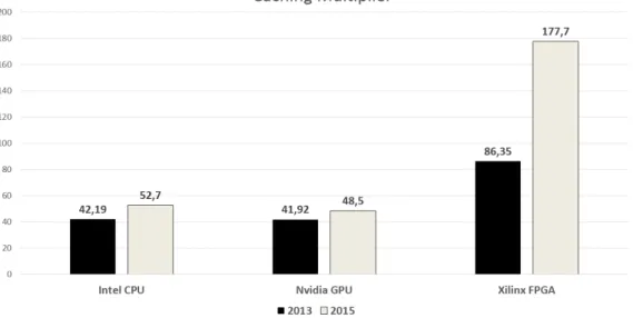
In 2013, all of the processor architectures suffer from memory bandwidth limitation. Two years later the problem is the same as can be seen in Table 2.2. Caching Multiplier can be the measure of memory bandwidth limitation because it shows the difference between computational capacity and the feeding capability of the memory interface. This mea- sure has become worse since 2013 (Fig. 2.1), especially for the FPGA. Intel, Nvidia and
8 2. BANDWIDTH LIMITATIONS IN MESH COMPUTING
Table 2.2. Bandwidth limitation of different architectures (2015) Chip (cores/threads) Bandwidth
Memory Type1 L2-L3 cache
GB/s MB
Intel i7-6700K 4.2 GHz (4/8) 34.1 DDR4 2x2133x64 8 Intel i7-5960X 3.5 GHz (8/16) 68 DDR4 4x2133x64 20 Intel E5-2699v3 3.6 GHz (18/36) 68 DDR4 4x2133x64 45 Nvidia Tesla K80 (4992 cuda cores) 480 GDDR5 12x2500x128 3.25
Xilinx VU13P (12288 DSP slices) 83.3 DDR4 4x2666x64 56.8
Chip (cores/threads) GFLOPS GFLOPS* Caching
Multiplier
Intel i7-6700K 4.2 GHz (4/8) 268,8 4.25 63.24
Intel i7-5960X 3.5 GHz (8/16) 448 8.5 52.7
Intel E5-2699v3 3.6 GHz (18/36) 504 8.5 59.29
Nvidia Tesla K80 (4992 cuda cores) 2910 60 48.5 Xilinx VU13P (12288 DSP slices) 1850 10.41 177.7 1 : Type (number of channels) x (Mega Transfers / s) x (bits)
GFLOPS* : if 1 MAC (2 FLOP) needs 2x8 byte input from main memory (no cache)
Figure 2.1. Caching Multipliers in 2013 and 2015.
Xilinx (and their competitors) reached great improvement on DP computing capability, while the memory bandwidth improvement was slighter. Nvidia seems to solve the prob- lem (doubled performance with doubled memory bandwidth), but the Tesla K80 is in fact two GK210 GPU with two instances of the GDDR5 interface of Tesla K20X. CPUs and FPGAs strengthen with the new DDR4 interface, but the bandwidth growth is less than the computational capacity growth as can be seen in Fig. (2.1). Xilinx ultrascale FPGAs can also use serial memory interface which consists 64 instances of 15 Gbps channels pro- viding 120 GB/s memory bandwidth. Xilinx improved the DP capability of the FPGAs
DOI:10.15774/PPKE.ITK.2016.007
with the new DSP48E2 slice which performs 27*18 bit multiplications at 891 Mhz thus the DP MAC units require less DSP slices. On the Xilinx VU13P chip, 1755 DP MAC units can be placed with 540 MHz maximum operating frequency. Even with the better 120 GB/s memory interface, more than 100 on-chip data reuse is necessary for the FPGA to reach the 100% utilization.
Processor architectures are bounded by the Speed (GFLOPS)—Power (Watt)—Area (die Table 2.3. Price and power efficiency of different architectures (2015)
Chip (cores/threads) Type Price Power Consumption DP Efficiency
USD Watt GFLOPS/Watt
Intel i7-6700K 4.2 GHz (4/8) CPU 350 91 2.94
Intel i7-5960X 3.5 GHz (8/16) CPU 1000 140 3.2
Intel E5-2699v3 3.6 GHz (18/36) CPU 3700 145 3.47 Nvidia Tesla K80 (4992 cuda cores) GPU 5000 2x150 9.7
Xilinx VU13P (12288 DSP slices) FPGA 20000* 40* 46.25*
*:based on approximations
mm2 or USD) triangle. Table (2.3) shows the main design aspects of different proces- sor types. High-end GPUs and CPUs utilize the maximum possible power (150 W) with market-driven chip sizes, while high-end FPGAs have 20.000 USD price and reach multiple times better theoretical power efficiency.
Current DRAM (Dynamic Random-Access Memory) technologies are DDR3-DDR4 and GDDR5. These memories are not fully random access because all of them use 8n prefetch- ing, which increases the theoretical memory bandwidth, but also increases the minimal amount of data per transmission. For DDR3, the access granularity is 8x(8-16) bit and 8x32 bit for GDDR5. In GDDR5X the 8n prefetch will be increased to 16n which results in higher theoretical bandwidth, but makes the interface more sensitive to small random memory transactions. DRAMs divide memory into banks, rows, and columns. Two con- secutive reads can take a different amount of time. The most efficient way to use a DDR memory is to read a row by burst reads, followed by reading an other row from a different bank, because banks work independently. While a bank closes a row, the other can opens one. With appropriate addressing (bank interleaving), this is a sequential memory read.
Any other memory access pattern have less utilized memory bandwidth than the theore- tical maximum.
Kilo-processor architectures are memory bandwidth limited, and heavy on-chip data reuse is necessary to provide input for PEs. Furthermore, the memory interface is sensitive to
10 2. BANDWIDTH LIMITATIONS IN MESH COMPUTING
small random accesses. Sequential memory access pattern is needed for maximum utiliza- tion of the off-chip memory bandwidth.
2.1.3. Possible Hardware Solutions to the Memory Wall
Better Memory Interface: Higher theoretical memory bandwidth is not enough, the access granularity, and latencies between random accesses are also important. With shorter transmission lines the frequency of the memory interface can be increased. Recent trends try to connect main memory and the processor through 3D via technology [R3, R4], which decreases the wire latencies and makes possible to create wide interfaces with 1024-2048 bits. While latencies drop down and theoretical memory bandwidth increases significantly, the sensitivity of the interface to random access patterns is still high.
Decreased Operating Frequency: Decreased frequency lowers GFLOPS of the pro- cessor. With the same memory interface this leads to better efficiency. Computational power linearly depends on the operating frequency, but the power consumption of a pro- cessor chip has quadratic frequency dependence. The main indicator of Green Computing GFLOPS/Watt becomes better if the frequency of the processor is decreased.
Increased On-Chip Memory: The rate of on-chip data reuse can be improved with increased on-chip memory. This approach can lead to better PE utilization, but increased on-chip memory needs more chip area, thus less PE can be placed on the same chip, which results in less GFLOPS.
Hardware manufacturers do extensive development to handle memory wall effect, but this is not enough. Software engineers have to use optimized memory access patterns.
2.2. Mesh Computing
Graphs often appear in scientific and industrial computational tasks. The spatial discre- tization of a 2D surface or a 3D volume can be represented by a graph. These graphs are called meshes and are used in numerical simulations of space-time behavior of sound, heat, elasticity, electrodynamics or fluid flow dynamics. From the design of an airplane to weather estimation, these simulations become the most frequent tasks on supercomputers.
DOI:10.15774/PPKE.ITK.2016.007
If the mesh has a uniform rule-based organization it is calledregular/structured, other- wise it is irregular/unstructured. Irregular meshes make possible the change of mesh density, which is beneficial in many cases. The same numerical precision can be achieved with an irregular mesh with much fewer elements than a regular mesh requires. However, computations on irregular meshes are more complex.
In mesh computing, the following questions arise: How to generate the mesh? (regu- lar/irregular, number of elements); How to partition a mesh for parallel computing? (opti- mization goals, partitioning method, number of parts); How to organize the corresponding data in main memory? In this work I deal with the second and third questions, further- more, I want to show that these two questions are in fact one.
In the later sections, I use the task of explicit numerical approximation of a system of
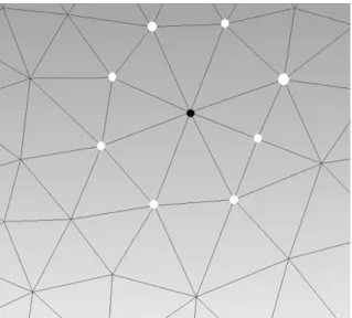
Figure 2.2. 2D vertex-centered mesh example. The black node depends on the white ne- ighboring nodes.
partial differential equations (PDE) where the spatial discretization is defined by a mesh.
The discretization is calledvertex-centered if the represented physical variable is defi- ned at the vertices. In the case of cell-centered discretization the represented physical variable is defined at the center of the primitive element (triangle, tetrahedron, etc.). The discretization stencildefines which neighboring elements and how contributes to the dy- namics of each element. The simplest discretization stencil contains the directly connected neighbors (Fig. 2.2), which has one distance from the current node in the graph.
12 2. BANDWIDTH LIMITATIONS IN MESH COMPUTING
2.3. Dataflow Computing
In dataflow computing, an operation is executed immediately if its operands are available.
In the case of classic von Neumann computing, an operation is executed when the serial control reaches the operation. The result of a dataflow operation can invoke multiple operations which can be executed in parallel. Dataflow computers are typically pipelined architectures in which a continuous data stream goes through an acyclic graph structure of operators.
Neumann machines often support SIMD (Single Instruction Multiple Data) computing to utilize multiple processing elements in parallel. Dataflow machines could provide the same extension with multiple identical pipes. This technique increases the input and output bandwidth requirements of the architecture, but gives linear speedup.
2.3.1. Dataflow computing on a mesh
As I mentioned in the previous section, in this work an explicit PDE solver is used as a test problem. In each time step, the state variables of all discrete mesh elements have to be updated. For the update, all the constants and state variables of the given node and its neighborhood are required. Mesh data have to go through the dataflow processor unit which can update a finite number of nodes at the same time. The necessary input has to be loaded on-chip for a node update, thus, all the required neighboring nodes have to be stored. The processor has finite memory resources which make a limit on the maximum distance of dependent nodes in the input stream, otherwise, the mesh data need to be loaded multiple times, and we lose most of the benefits which come from the dataflow concept.
Fig. (2.3) shows the memory transfers in the case of a dataflow machine that works on
Figure 2.3. Linearized mesh data goes through on-chip memory buffer.
mesh data. First, the mesh elements have to be ordered into a serial stream, which goes
DOI:10.15774/PPKE.ITK.2016.007
through an on-chip memory buffer, from which the dataflow arithmetic can access the required data for a node update. Ordering is a key step for dataflow computing because the ordering defines the maximum distance of dependent elements in the stream. If we see the adjacency matrix of the graph, this distance is equal to the largest distance of nonzeros in a row of the matrix. If we consider always updating the middle element of the on-chip memory buffer, this distance is two times the largest distance of a nonzero from the main diagonal, which distance is called graph or matrix bandwidth (G BW). The size of on-chip memory buffer gives an upper bound on possible graph bandwidth.
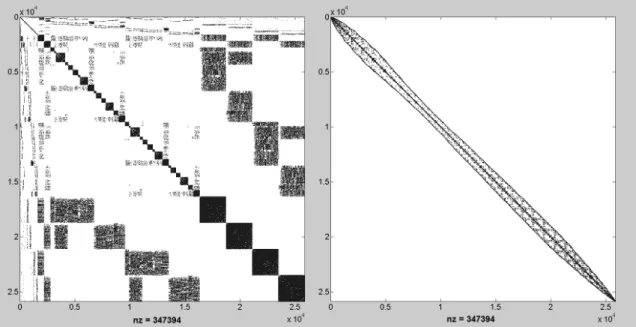
An ordering is required which results in less G BW than a bound. There are effective matrix bandwidth minimization heuristics, however, to find an optimal ordering is NP- complete. In Fig. (2.4) the adjacency matrix is shown for the same graph before and after reordering. Reordering heuristics like Cuthill-McKee or GPS are effective and fast, but it is possible that a graph can not be reordered under a given G BW bound. In later chapters, I will give some possible solution to this problem.
Figure 2.4. Nonzero elements position in the adjacency matrix of a mesh before (left) and after (right) reordering. The two matrices represent the same mesh with different node ordering, thus the number of edges (nz) remains the same. Node reordering can decrease the graph bandwidth significantly.
14 2. BANDWIDTH LIMITATIONS IN MESH COMPUTING
2.3.2. Memory access optimization and interprocessor communication
Optimized memory access is essential for high processor efficiency. Current mesh partit- ioning methods focus only on inter-processor communication, however, processor-memory communication is also critical for recent processor architectures. This contribution sug- gests considering the properties of inter-processor and processor-memory interfaces with the processor’s caching capability in mesh partitioning.
Dataflow Computing is a possible solution for memory wall effect because it requires a continuous input data stream. Streams have fully sequential memory access pattern, which means optimal memory bandwidth efficiency. Recently, Dataflow Machines are introduced for explicit PDE computations on structured [R13] and unstructured [J1] meshes, and they are proved to be much faster than any other architecture.
The benefits of these architectures can be exploited only if the input stream has optimized data locality. A segment of the input stream can be cached in the on-chip memory. Howe- ver, all data dependencies have to be inside a segment. The size of the available on-chip memory defines an upper bound (BW Bound) on the maximum distance of dependent data in the stream. This is a hard constraint. If dependent data have greater distance in the stream than the bound, DM can not handle it.
Inter-processor communication is also important for Dataflow Machines. If the processors have to wait for data from the inter-processor communication channel, the efficiency also becomes lower. To evade this effect, Eq. (2.1) must be considered, which defines a bound (COM M Bound) on the ratio of inter-processor communication.
communication [byte]
input for computation [byte] ≤ inter-processor bandwidth [byte/s]
off-chip memory bandwidth [byte/s] (2.1) COM M Bound is defined by the ratio of the inter-processor and off-chip DRAM bandwidth. In [J1] Alpha-Data ADM-XRC-6T1 cards are used which provide 12.5 GB/s theoretical off-chip memory bandwidth, and 1.25 GB/s bandwidth between the cards, thus COM M Bound= 0.1. In [R13] two custom PCI Express add-on cards are presented. The first has 9.375 GB/s off-chip memory bandwidth with 2.5 GB/s inter-processor bandwidth, which results COM M Bound = 0.26. The second configuration has 37.5 GB/s off-chip memory bandwidth with 5 GB/s inter-processor bandwidth, thusCOM M Bound= 0.13.
DOI:10.15774/PPKE.ITK.2016.007
2.3.3. Data Locality in Mesh Computing
A graphGcan be associated to each mesh, by converting each mesh element to a vertex, and each face to an edge. In the case of an explicit PDE solver, data locality is the maximum distance between adjacent nodes in the linearized stream of mesh data. This distance is proportional to Bf(G), which is is the graph bandwidth of G according to node ordering f (details in Sec. 4.3). Data dependencies in the numerical method are described by the discretization stencil. When the discretization stencil includes only the adjacent elements, its width is s = 3. With these notations, the maximum distance of dependent nodes is (s−1)·Bf(G) + 1. Multiple explicit iterations can be computed with one off-chip read if the intermediate results are also stored in an on-chip buffer, and the dataflow arithmetic units are connected in a pipeline [J1]. The relation between the graph bandwidth and the BW Boundis given in Eq. (2.2).
Iterations· {(s−1)·Bf(G) + 1} ≤BW Bound (2.2) BW Bound is determined by the maximum size of available on-chip memory. Data Locality bounds are 30-90K and 40-300K for architectures described in [J1], and [R13], respectively.
Minimization of the graph bandwidth can provide data streams with feasible data locality.
The goal of minimization is to find an ordering f, for which the graph bandwidth is minimal. The achievable minimal graph bandwidth depends on the graph. A partitioning method defines subgraphs, which affect the achievable graph bandwidth. This effect is investigated in Section 4.3.
Data locality (BW Bound) and inter-processor communication (COM M Bound) have to be considered together in mesh partitioning. In the following chapter, an overview is given on existing dataflow architectures which can utilize my results on data locality based mesh partitioning.
DOI:10.15774/PPKE.ITK.2016.007
3. Chapter
Dataflow Machines
This chapter gives an overview on existing dataflow machine architectures of different application areas. The case of mesh computing is presented in more details through two special-purpose dataflow machines.
3.1. FPGA and All Programmable System on Chip (APSoC) architectures
Dataflow machines require high hardware flexibility which can be only achieved by ASIC or FPGA chips. Before I introduce DM applications, I give a brief overview of FPGA and APSoC architectures through Xilinx products.
3.1.1. Field Programmable Gate Array (FPGA)
The evolution of FPGA chips has started from real logic gate arrays (Field Programmable Logic Array—FPLA) and has shifted towards more complex building blocks. The current FPGA technology is grounded on the LCA (Logic Cell Array) architecture which is int- roduced by Xilinx in 1985 [R14]. This minimal design has a grid of logic cells which is surrounded by Input/Output Blocks (IOB). The LCA has a programmable interconnect between all elements. Each logic cell consists a logic function generator and 1-bit stor- age (flip-flop).
Later, more complex and special building blocks appear in the Virtex architectu- re (Fig. 3.1). Logic cells evolved to Configurable Logic Blocks (CLB) that consists 4 Lok-Up Tables (LUT), 4 Carry generators and 4 flip-flops as it can be seen in Fig. 3.2. CLBs form
17
18 3. DATAFLOW MACHINES
Figure 3.1. The Virtex Architecture ([R14]).
a grid, which is surrounded by IOBs. IOBs are connected to the CLB matrix through special programmable interconnect (I/O Routing) while CLB-CLB connections are provi- ded by the General Routing Matrix (GRM). The new Delayed Locked Loop (DLL) blocks are responsible for clock handling, and dedicated memory units are also added to the dsign (Block RAMs). Each BRAM module is a 4 Kbit dual-port RAM with independent control signals and configurable data width. LUTs in CLBs are not only function genera- tors, but they can also be used as RAMs or shift registers. CLBs can perform full-adder logic and multiplexing.
The key ability of FPGAs is the programmable hardware connections. Fig. (3.3) shows
Figure 3.2. 2-Slice Virtex CLB ([R14]).
DOI:10.15774/PPKE.ITK.2016.007
the direct connections between neighboring CLBs and GRM crosses. Each programmable wire cross adds a delay to the signal path, thus long range and mid range lines are also added to the design for routing long-distance paths.
In later generations, the size of LUTs and BRAMs increased, and new blocks appeared
Figure 3.3. Local interconnects in a Virtex FPGA. ([R14]).
such as DSP slices and dedicated Ultra RAMs. Based on the most common applications, more and more functionalities got dedicated support on the chip. For instance, in ultra- csale FPGAs the BRAMs have dedicated cascade support as it can be seen in Fig. (3.4).
Because of the demand for larger on-chip memory, Xilinx added a new type of memory resource which is called Ultra RAM. Ultra RAMs have less reconfigurability than Block RAMs, but they are perfect for larger on-chip memory formation. Ultra RAM has 288 Kbit memory in a single block and dedicated cascade support as BRAMs.
The most important module in the case of High-Performance Computing (HPC) is the DSP slice because it can perform multiplications. Fig. (3.5) shows the DSP48E2 slice of the ultrascale family. As I mentioned in the previous chapter, this module performs 27*18 bit multiplications at 891 Mhz. One of the benefits of FPGAs is custom precision compu- ting, however, the need for standard double precision in real applications forces Xilinx to increase the bit width of the multiplier.
20 3. DATAFLOW MACHINES
Figure 3.4. Dedicated Block RAM Cascade in UltraScale Architecture ([R15]).
Figure 3.5. Enhanced DSP in UltraScale Architecture ([R15]).
3.1.2. All Programmable System on Chip (APSoC)
Complex applications require different types of computing functionalities. Hybrid archi- tectures are developed to handle these challenges. Here I show the Zynq 7000 APSoC chip (Fig. 3.6) which consists a dual-core ARM Cortex-A9 processor (Processing System—
PS) and a 7th series Xilinx FPGA part (Programmable Logic—PL).
DOI:10.15774/PPKE.ITK.2016.007
Figure 3.6. Zynq-7000 All Programmable SoC Overview ([R16]).
The PS side of the chip can replace the host CPU and can communicate with the FPGA part on-chip. The PS side can be programmed in C, and the Vivado toolchain generates the necessary drivers for the custom logic on the FPGA side which makes the APSoC easy to use. The benefits of custom FPGA cores and a standard ARM CPU are joined. 32/64 bit AXI4 interfaces to connect the different types of custom PL modules and the PS. As shown in Figure (3.7), these interfaces connect the PL to the memory interconnect via a FIFO controller. Two of the three output ports go to the DDR memory controller, and the third goes to the dual-ported on-chip memory (OCM).
The PS side runs at maximum 1 GHz while the FPGA part maximum frequency is based on the application (250 MHz for Zynq PS AXI interface). If the application can utilize the parallel computing capabilities of the PL side the result is a power-efficient high-performance design.
22 3. DATAFLOW MACHINES
Figure 3.7. PL Interface to PS Memory Subsystem ([R16]).
3.2. Existing hardware solutions of DMs
The following examples represent the common application areas and hardware solutions of dataflow machines. Except the NeuFlow ASIC implementation, all of these architectures are realized on FPGA chips.
3.2.1. Maxeler accelerator architecture
This architecture could be the general framework example. The DM is placed on an FPGA-based accelerator board which is connected to a general purpose CPU host through PCI Express.
The application kernel is transformed automatically from a dataflow graph into a pipelined FPGA architecture, which can utilize a large amount of the parallel computing resources on the FPGA chip. The host application manages the interaction with the FPGA accelerators while the kernels implement the arithmetic and logic computations in the algorithm. The manager orchestrates data flow on the FPGA between kernels and to/from external interfaces such as PCI Express. In [R17] this architecture is used for resonance-based imaging in a geoscientific application which searches for new oilfields.
The implementation involves 4 MAX3 FPGA accelerator cards. Each card has a lar- ge Xilinx Virtex-6 FPGA and is connected to the other FPGAs via a MaxRing connection.
DOI:10.15774/PPKE.ITK.2016.007
Figure 3.8. Maxeler accelerator architecture ([R17]).
3.2.2. HC1 coprocessor board
In paper [R18], the authors present an accelerator board which is made for the investiga- tion of evolutionary relations of different species. The computational problem includes a maximum likelihood-based phylogenetic interface with the Felsenstein cut method. BE- AGLE is a programming library which contains phylogenetic algorithm implementations for many architectures. This library is also extended to FPGA platforms which name is Convey HC-1.
The corresponding hardware solution is based on a Xeon server CPU host with 24 GB memory. The accelerator includes 4 Virtex-5 FPGAs, which can access 16 GB on-board memory through a full crossbar network (Fig. 3.9). The FPGAs have a ring topology inter-FPGA communication network. When the input problem is distributed among the FPGAs, the topology has to be considered, because the communication between neighbors is multiple times cheaper than the communication of 2 FPGA-s which are not adjacent.
The large on-board memory makes possible to ignore the relatively slow PCI Express interface during the computation.
24 3. DATAFLOW MACHINES
Figure 3.9. The HC1 coprocessor board. Four application engines connect to eight memory controllers through a full crossbar ([R18]).
3.2.3. Multi-Banked Local Memory with Streaming DMA
In the project that is shown in [R19] a special on-chip memory organization is used. The multi-way parallel access memory is a perfect solution to feed the dataflow arithmetic.
The on-chip memory is filled by a streaming DMA which reads the off-chip memory con- tinuously. This DMA strategy utilizes the whole off-chip DRAM bandwidth which is the limiting factor in many applications.
Figure (3.10) shows the organization and connections of an Application-Specific Vector Processor (ASVP). Each ASVP has a simple scalar processor (sCPU) for scheduling the vector instructions (α), for programming the streaming DMA engine (γ) and for optional synchronization with other ASVPs through Communications Backplane (δ). The vector instructions are performed by the Vector processing Unit (VPU) which can access the BRAM-based Local Storage banks in parallel (β). The maximal operating frequencies of the VPU are 166MHz, 200MHz, and 125MHz, for Virtex 5 (XC5VLX110T-1), Vir- tex 6 (XC6VLX240T-1), and Spartan 6 (XC6SLX45T-3) FPGAs, respectively.
Multiple ASVPs can be connected to the streaming memory interface, if there is enough resource on the FPGA and there is enough off-chip memory bandwidth. For different app-
DOI:10.15774/PPKE.ITK.2016.007
lications, only the Vector Processing Unit has to be changed, most of the architecture can be unchanged which saves development cost.
Figure 3.10. A system-level organization of an Application-Specific Vector Processor core ([R19]).
3.2.4. Large-Scale FPGA-based Convolutional Networks
An important application area is the 2D or higher dimensional convolutions. These comp- utational tasks appear in almost all image or video processing applications, and they are computationally expensive. In Fig. (3.11) the architecture of [R21, R20] is shown when it is configured for a complex image processing task. The processor is formed by a 2D matrix of processor blocks. Each block has 6 predefined computing module with independent in/out interfaces which can be connected optionally through a connection matrix. In the given example, the 3 upper blocks perform a 3x3 convolution while the middle 3 block perform another 3x3 convolution. The two results are added by the left down block, and then the down center block computes a function.
In Fig. (3.12) can be seen the manufactured chip layout. It is interesting that the streaming part is as large as the computing part on the chip. The flow CPU is used for programming
26 3. DATAFLOW MACHINES
Figure 3.11. NeuFlow application example ([R20]).
the other parts and makes possible fast reconfigurations during the computation.
Figure 3.12. Chip layout in a 2.5×5mm2 die area ([R20]).
3.2.5. Pipelined Maxeler Accelerators
This architecture is based on the one mentioned in [R17]. Fig. (3.13) show the Maxeler MPC-C architecture and the corresponding design flow. The usage of dataflow machines becomes much easier with the projects like Maxeler, which provides frameworks which requires only C-like programming skills, and generates the hardware description codes automatically. In the paper [R22] this architecture is used for electromagnetic field simu-
DOI:10.15774/PPKE.ITK.2016.007
Figure 3.13. MPC-C platform architecture and Maxeler design flow ([R22]).
lations. The host consists general purpose CPUs (two Intel Xeon X5650 2.7GHz 6-core CPUs), which communicate with FPGA-based boards (four MAX3 DFE cards) through PCI Express. The FPGAs has their DRAM, and they are connected in a ring topology.
Here I want to show the possibility of deep pipelining. In the case of an iterative method, the operations of one iteration can be copied after each other or with timesharing and data back feeding multiple iterations can be computed without off-chip memory transfers.
The Figure (3.14) shows the possible pipelining depths. The electric (E) and magnetic (H) fields can be computed in two steps on the same processor unit (a). E and H can be computed in a pipeline which means two times speedup with two processor units (b), and if there are enough resources, more iterations can be performed at once with deep pipelining (c).
28 3. DATAFLOW MACHINES
Figure 3.14. Possible pipelined approaches. (a) no pileline (b) single iteration (c) multiple iterations ([R22]).
3.3. Off-chip memory streaming techniques
This section gives an overview of the three most common streaming techniques between main memory and the dataflow processor unit. In [R23] the authors did experiments based on the Himeno benchmark which is frequently used in performance evaluation. The met- hod is named after Dr. Ryutaro Himeno and includes the Jacobi iteration based solution of the Poisson equation which is part of the Navier-Stokes equations.
For the investigations, the MAX3 acceleration card was used which has a Virtex-6 SX475T
Figure 3.15. Direct feed from host main memory through PCI-Express ([R23]).
DOI:10.15774/PPKE.ITK.2016.007
FPGA, 24GB DDR3 memory and PCI express gen2 x8 interface. On the FPGA multiple dataflow solver units (pipe) can be implemented. The number of pipes is limited by the logic resources of the FPGA, however, these pipes require high memory bandwidth.
In the benchmark problemNpdenotes the number of sample points in the 3D spatial doma- in, where the pressure (p) must be determined in each iteration. The number of iterations is nnthusNp×nndata elements must be communicated during the computation. The tests are done for 3 different sized problems: S 65x65x129 (2.1 MB), M 129x129x257 (16.3 MB) and L 257x257x513 (129.3 MB). The clock speed of FPGA designs is set to 100 MHz.
The first possible way of streaming is the direct feed from the main memory of the host through the PCI-Express bus as we can see in Fig. (3.15). In this case, only 8 pipes can be supplied because the PCI Express memory bandwidth limits the performance at 8.33 GFLOPS.
The other extreme case when the whole problem is placed in an on-chip memory buffer.
Figure 3.16. Input loaded to on-chip local memory and processors feeded from on-chip memory ([R23]).
It is viable only for small problems (S data set) because the on-chip memory need is re- lative to the size of the problem, but this case shows the maximal performance available.
Figure. (3.16) shows the block diagram and figure (3.17) the measurement results, which indicates 145 GFLOPS at only 100 Mhz with 48 parallel pipes. The design with 48 pipes could run at maximum 110 MHz which results in 155 GFLOPS peak performance.
30 3. DATAFLOW MACHINES
Figure 3.17. Results of on-chip buffer feeding ([R23]).
The on-board 24 GB DDR memory can handle relative large problems and can also exc-
Figure 3.18. Input loaded to on-board DRAM and processors feeded from on-board me- mory through off-chip memory interface ([R23]).
lude the slow PCI Express bus (Fig. (3.18)). In the beginning, the input data is loaded to the on-board DDR and after the whole computation, the final result is sent back to the host. In this case, the FPGA has to include memory address generators which consume resources thus only 32 pipes can be implemented. The peak performance is 97,6 GFLOPS (Fig. (3.19)), however, this approach is applicable for large problems as well. In high- performance computing, this technique is the most common to feed dataflow processors.
DOI:10.15774/PPKE.ITK.2016.007
Figure 3.19. Results of the on-board memory feeding ([R23]).
In the following section, two special-purpose mesh computing dataflow machines are int- roduced, and both of them use the on-board DDR memory streaming.
3.4. Special-Purpose DMs for mesh computing
The following two architectures are specialized for mesh computing. Both of them have found to be the best architectures in the case of explicit PDE computing, because of the total off-chip memory bandwidth utilization [R13, J1]. The previous chapter has given an introduction to these special DMs.
3.4.1. DM for structured meshes
The Maxeler framework has been mentioned multiple times in this chapter. Here I show the application of [R13] and focus on the case of distributed mesh computation on mul- tiple DMs. The corresponding hardware solution includes 4-16 FPGA-based accelerators which are connected to the host through PCI Express and has a ring topology intercon- nection network. Each FPGA (Dataflow chip) has its on-board memory as can be seen in Fig. (3.20).
The input is a 3D structured discretization of a rectangular space domain. Fig. (3.21) shows the distribution of the domain among the DMs. The domain has been cut according to one dimension into equal sized pieces. This distribution is ideal for the ring topology, furthermore, if the DMs are synchronized, they can share the boundary cell information
32 3. DATAFLOW MACHINES
Figure 3.20. Architecture of a compute node. Each of the Data-Flow Engines (DFE) is con- nected to the CPUs via PCI Express and has a high bandwidth MaxRing interconnection to its neighbors ([R13]).
Figure 3.21. One-dimmensional decomposition of the problem domain to parallelize across multiple DFEs linked with MaxRing ([R13]).
with each other without extra off-chip memory transfers. This architecture also has a data locality limit which comes from the available memory resources on the FPGA chip, as it has been mentioned in Sec. (2.3).
DOI:10.15774/PPKE.ITK.2016.007
3.4.2. DM for unstructured meshes
Figure 3.22. Block diagramm of the proposed dataflow processor unit ([J1]).
The main difference between structured and unstructured mesh computing is the additional knowledge of neighbors in the structured case. For unstructured meshes connectivity is not a trivial rule, it has to be stored and transferred to the processor unit. In Fig. (3.22) the dataflow processor unit of [J1] is shown with its input and output channels. During the explicit PDE computation, the corresponding state variables have to be updated at each mesh element at every timestep. Connectivity descriptors are also transferred through off-chip memory interface to a local address generator module which addresses the processor’s Memory Unit which is a large FIFO that is filled continuously with mesh data.
Multiple dataflow processor units can be placed in a chain if there are enough resources on the FPGA chip. Fig. (3.23) presents the complete architecture with multiple pipelined processors on the same FPGA. The deeper levels need their memory units thus the increased number of these modules makes harder the limit on data locality. If data locality can be optimized better, it allows the usage of deeper pipelining on the same FPGA.
The arithmetic is pipelined according to the dataflow graph of the numerical algorithm.
In the presented 2D cell-centered problem, each cell (triangle) has three interfaces, and the state variables are updated based on a flux function computed at the three interfaces.
(For mathematical formulation, see [J1]) This arithmetic is optimized to reach the highest
34 3. DATAFLOW MACHINES
Figure 3.23. Outline of the proposed architecture. The processors are connected to each other in a chain to provide linear speedup without increasing memory bandwidth requi- rements. The number of processors is only limited by the available resources of the given FPGA ([J1]).
Figure 3.24. A partitioned data-flow graph generated from an explicit PDE solver numeri- cal method and partitioned with the algorithm described in [R24]. Each part has its own local control ([C1]).
possible operating frequency. The dataflow structure is partitioned as can be seen in Fig. (3.24) where each part has its local control.
DOI:10.15774/PPKE.ITK.2016.007
3.4.3. Implementation of the DM for unstructured meshes
In the project of [J1] I was responsible for the memory bandwidth optimization part, which was performed by a special mesh node reordering and virtual partitioning method.
In this section, I present our implementation results on an AlphaData ADM-XRC-6T1 reconfigurable development system equipped with a Xilinx Virtex-6 XC6VSX475T FPGA and 2 Gbyte on-board DRAM. This FPGA architecture was introduced in 2010, thus its performance is compared to the CPU and GPU architectures from 2010. I also investigate the effect of increased data locality on CPU and GPU performance.
The architecture was implemented using Xilinx and AlphaData IP cores at double pre- cision. The optimized arithmetic unit for dissipation-free, inviscid, compressible fluid dy- namics computation (cell-centered 2D) had 325 MHz maximum clock frequency. The AU performs a cell update in 3 clock cycles. Computation of each new state value requires loading and storing of one state variable vector (2x32 byte), loading of the area of the tri- angle (8 byte), and loading of three connectivity descriptors (3x26 byte) that are 150 byte altogether. Therefore, a 16.3 Gbyte/s memory bandwidth is required to feed the processor with valid data in every third clock cycle. However, our four 32-bit wide memory banks running on 800 MHz providing 12.8 Gbyte/s peak theoretical bandwidth. This limitation can be removed by slightly modifying the architecture shown in Figure (3.23) and con- necting two Memory Units to one AU creating two virtual processors. One Memory unit is enabled in even clock cycles, whereas the other is enabled in odd clock cycles. In this case, one physical AU computes 2 time iterations, thus the necessary input bandwidth decreases to 8.2 Gbyte/s. This technique requires more on-chip memory resources for each physical AU, thus the data locality requirement of the dataflow architecture increases. It means that the mesh elements have to be reordered to provide lower graph bandwidth.
Table (3.1) summarizes the resource needs of the architecture that is shown in Fig. (3.22).
Table 3.1. Area requirements of the architecture.
DSP LUT FF
Number of elements 525 43754 61936 XC6VSX475T utilization 26% 14.7% 10.4%
The most limiting factor is the number of DSP slices which enables 3 physical AUs on the Virtex-6 XC6VSX475T FPGA. In case of three processors, maximum bandwidth of
![Figure 3.1. The Virtex Architecture ([R14]).](https://thumb-eu.123doks.com/thumbv2/9dokorg/1303826.104899/34.892.274.579.155.459/figure-the-virtex-architecture-r.webp)
![Figure 3.5. Enhanced DSP in UltraScale Architecture ([R15]).](https://thumb-eu.123doks.com/thumbv2/9dokorg/1303826.104899/36.892.118.714.604.855/figure-enhanced-dsp-in-ultrascale-architecture-r.webp)
![Figure 3.6. Zynq-7000 All Programmable SoC Overview ([R16]).](https://thumb-eu.123doks.com/thumbv2/9dokorg/1303826.104899/37.892.159.783.135.643/figure-zynq-all-programmable-soc-overview-r.webp)
![Figure 3.8. Maxeler accelerator architecture ([R17]).](https://thumb-eu.123doks.com/thumbv2/9dokorg/1303826.104899/39.892.213.725.180.593/figure-maxeler-accelerator-architecture-r.webp)
![Figure 3.9. The HC1 coprocessor board. Four application engines connect to eight memory controllers through a full crossbar ([R18]).](https://thumb-eu.123doks.com/thumbv2/9dokorg/1303826.104899/40.892.139.713.147.534/figure-coprocessor-application-engines-connect-memory-controllers-crossbar.webp)
![Figure 3.10. A system-level organization of an Application-Specific Vector Processor core ([R19]).](https://thumb-eu.123doks.com/thumbv2/9dokorg/1303826.104899/41.892.261.658.241.624/figure-level-organization-application-specific-vector-processor-core.webp)
![Figure 3.11. NeuFlow application example ([R20]).](https://thumb-eu.123doks.com/thumbv2/9dokorg/1303826.104899/42.892.178.667.152.548/figure-neuflow-application-example-r.webp)
