A Hardware Platform for Frequency Domain Spectroscopy and Frequency Response Analysis
Jan Tomlain, Ondrej Teren, Radek Sedlacek, Josef Vedral
Department of Measurement, Faculty of Electrical Engineering, Czech Technical University in Prague, Technicka 2, 166 27 Prague 6, Czech Republic
tomlajan@fel.cvut.cz, terenond@fel.cvut.cz, sedlacr@fel.cvut.cz, vedral@fel.cvut.cz
Abstract: This paper describes a development of a hardware platform suitable for the frequency domain spectroscopy (FDS) and frequency response analysis (FRA) applied for high-voltage machine diagnostics. The principle of the FDS and FRA methods widely used by maintenance technicians are briefly reviewed. Important technical requirements for the instruments utilizing these methods are stated. A design of a hardware platform with parameters fitting both of the method and engagement of the latest electronics components is discussed. In order for verification of the design platform, a basic implementation of a vector voltmeter is described. Long-term stability, phase shift sensitivity, and accuracy of the platform are evaluated.
Keywords: high-voltage machine diagnostics; dielectric spectroscopy; dielectric response analysis; frequency response analysis; non-invasive diagnostic; machine insulation; lock- in amplifier
1 Introduction
In the field of energetics, there are a number of high-voltage (HV) machines. As an example, power transformers and generators directly used in the production and the transmission of electricity, should be mentioned. The lifetime of the machines are expected to be decades. To achieve the expected lifetime it is necessary to plan the regular diagnostic examinations of these machines. Thus, the machine operator avoids an unexpected shutdown of the machine or the entire system [1]. In many cases, the power transformer can work in relatively good conditions even if they exceeded their operational lifetime [2]. Therefore, it is not economically effective to replace such machines solely because of exceeding their expected lifetime. This fact is another reason to develop a non-invasive assessment method of the machines.
HV machines windings and their insulation systems are constantly exposed to a combination of heat, electric and mechanical stresses [3], [4]. All of these factors have an influence on the state of the machines winding insulation. The state of winding insulation is one of the studied parameters that can detect an upcoming failure. There are few measurement methods used in winding insulation state assessment, such as: electric resistance measurement using DC current [5], partial discharge measurement [6], [7], dielectric response measurement [8], capacitance, and dissipation factor measurement measured at power grid frequencies, dielectric spectroscopy [9] and frequency response analysis (FRA) [10]. The stresses mentioned above and also aging and moisture generation induced by these stresses have an influence on the conduction and the polarization processes inside the insulation material.
This paper further deals with FDS and FRA diagnostic methods. Common hardware requirements for both methods are found, such as: (parameters of excitation signals of a device under test and sampling frequencies of the measurement of device response). Baseed on these requirements, a design of a hardware platform intended for the mentioned methods is described. The primary goal of this work is development of an instrument fully suitable for practical measurements utilizing the FDS and FRA methods. Another objective of this work, is also an effort to increase the accuracy of the measurement and improvement of parameters (frequency range, excitation voltage level, resolution, linearity, etc.) in comparison with other instruments available in the market.
2 Frequency Domain Spectroscopy
Frequency domain spectroscopy (FDS) is one of the methods suitable for studying polarization phenomena. Every kind of insulation material consists, at an atomic level, of negative and positive charges. The charges are balancing each other, and on the macroscopic level, they produce a neutral charge. When applying an external electrical field E the charges become oriented thus, formate dipoles. The positive charges are attracted to the negative pole and vice versa. This phenomenon is called the polarization.
FDS is a method that utilized an AC current excitation of studied material (transformer insulation). The capacitance and the dissipation factor are measured as a function of frequency of the excitation signal [11], that can be expressed using an equation
( ) U ( )
I j C
(1)where I(ω) is the measuring current, C(ω) is the capacitance of the measured material sample U(ω) is the excitation voltage. The frequency range is usually between 1 mHz and 1 kHz, and a voltage level of hundreds of volts is needed [12].
A base block diagram of an FDS analyzer with a typical connection to a device under test (DUT) is shown in Fig. 1.
Figure 1
The block diagram of the dual channel FDS analyzer
The DUT is represented by a transformer with a primary winding H and two secondary windings A and B. There are also shown parasitic capacitances CHA, CHB and CHG that can be measured using the FDS analyzer. The FDS analyzer consists of a frequency sweep generator (FSG), a high-voltage amplifier and two ammeters. The FSG generates a sinus waveform with an adjustable frequency.
This signal is amplified using the high-voltage amplifier to an amplitude of hundreds of volts. A studied parasitic capacitance of the DUT is excited by the amplified signal. A current flowing through the studied capacitance is measured by the ammeters. In order to perform the computation of capacitance and dissipation factor, it is necessary to measure both the current amplitude and the current phase with respect to the generating signal. The measured parameters are calculated using the equation (1). A typical dissipation factor course measured using the FDS method is shown in Fig. 2.
Figure 2
The typical FDS measurement result and factors affecting the dissipation factor, similar picture in [12]
3 Frequency Response Analysis
The motivation for the FRA measurements is very similar to the methods mentioned above. Many dielectric and mechanical failures in power devices like transformers are caused by mechanical changes in the winding structure. These defects, or displacements in the winding structure, may be the result of transportation damage occurring between the manufacturer and the installation location. Moreover, also powered devices by this particular transformer could cause defects. For instance, low impedance fault on these devices could be harmful [10]. Common problems are also natural effects of the insulation aging.
Early detection of these displacements of a dielectric failure can reduce unplanned maintenance costs and provide the possibility of improving system reliability by preventing these failures. In addition, when the damage is discovered, repairs may be targeted to a specific place.
3.1 Theory
The main idea behind the FRA process is to measure the transfer function of the inspected subsystem in some frequency span. Inputs and outputs of the particular transfer function can be freely chosen to obtain various data.
Diagnostic result for the high voltage machinery FRA, is typically a relation between the impedance of the DUT as a function of the excitation frequency. The typical frequency range according to [10] is from 10 Hz up to 5 MHz. It has been verified that even minor displacements in the geometric structure of the large power transformer windings or changes in the dielectric parameters of the insulation system will lead to the relevant changes in the FRA fingerprint. This fact supports the results from simulations in [10] and [13]. To understand even better the relationship between the transfer function estimation and the transformer physical changes [13] provides a simplified equivalent schematic of the transformer with explanation of what value is changed, by what defect. A useful overview of these changes is documented in [14].
3.2 Swept Frequency Method
The first method, known as the swept frequency response analysis (SFRA) method, uses the fact that the impedance (or admittance) of a transformer winding varies with the frequency. A basic connection is shown in Fig. 3. The FRA analyzer could be substituted with a network analyzer for simplicity. DUT is excited with AC voltage with amplitude in a range of tens of volts, acc. to [10].
There is another voltage probe to measure actual voltage present on the DUT terminal. This connection eliminates any mistakes caused by testing voltage cable wiring. Current flown from neutral terminal of the DUT is the output measured
value. The input impedance of the network analyzer could be used to convert resulting current from the neutral terminal to the voltage as shown in Fig. 3.
Despite the simple data analysis, there are several disadvantages of this method.
At very low frequencies (in the range of some hundreds of Hz up to low kHz), these instruments tend to lack sufficient power to appreciably excite a large power transformer, due to the heavy inductive load presented by the steel core. This problem is described more deeply in [10]. The fixed sensing impedance of 50 Ω could be insufficient to convert the current signal in the whole frequency range properly. However, main advantages are simple hardware connection, easy data analysis processes and possible usage of instruments like network analyzers. On the other hand, disadvantages are in sensing impedance selection, cable length and connections, together with repeatability issue. A significant performance obstacle is an insufficient power to gain proper excitation of HV machines in the whole frequency range. SFRA method testing together with results is described in [15]
and [16].
Figure 3
Typical test connection for a low voltage SFRA
3.2.1 Measuring Principle
The FRA instrument that is using the classical SFRA must measure two voltage signals, in which one corresponds to the voltage on the input phase terminal and the second one on the sensing impedance, which corresponds to the current-flown through DUT. The simplified electrical schematic is shown in Fig. 4.
Figure 4
Measurement principle of DUT impedance
Impedance is then given by:
sense sense in
sense DUT
U U R U
I
Z U
(2)3.3 Traditional Impulse Method
In contrast with, the previous method, the impulse method tries to compensate several imperfections of the swept mode. The basic principle is described in [10]
and especially in [14]. Measurement is done in a frequency domain with single impulse transition response analysis. A test connection for the impulse measurement is shown in Fig. 5. A network analyzer is altered by the impulse generator with a high-speed digitalization unit. The main idea behind this measurement is to produce a single low voltage impulse to one terminal of the DUT and measure particular response to this impulse on the neutral terminal.
Similarly, the current on the neutral terminal should be properly converted to the voltage. There is a possibility to use another value of the sensing impedance in contrast with internal one in the network analyzer. Once the time domain record of the voltage (input) and current (output) are recorded, the transfer function is calculated as the Fast Fourier Transform (FFT) of the output divided by the FFT of the input. Unfortunately, this method has also its limitation. There are several practical problems which cause difficulties with the repeatable results together with the accuracy aspect. Present noise in the signal has a negative effect on the final FFT result. Easiest elimination is to apply averaging of more than one result.
This is one of the recommendations in [10]. A good level of repeatability is limited by another two factors. Test impulse should be the same for each single measurement of the averaged set. The second, is the quality and performance of the digitalization unit. The Impulse FRA method testing together with results is described in [17] and [18].
Figure 5
Typical test connection for a low voltage SFRA
4 Designed HW Platform
The FDS and FRA methods described in Chapters 2 and 3 do have some common attributes. Both of the methods require a generation of an excitation signal and a measurement of the DUT response. The measurement is based on sampling the response signal, but the signal processing itself is different for both methods.
However, there is a possibility to integrate both methods and implements of them into one platform.
Hardware for the whole diagnostic process consists of three main parts, see Fig. 6.
A core part of the digital signal analysis is an FPGA board, a data conversion and acquisition is done on an analog daughterboard. A coupling front-end board provides a power front-end to amplify signals generated by the daughter board.
The coupling front-end is designed to operate with excitation signal with a voltage of 30 Vpp and fulfills requirements of the excitation signal in case of FRA method. Thus, then a chain of FPGA board, daughter board and coupling board forms whole FRA instrument. In the case of the FDS method, an external HV amplifier is needed that is not discussed in this paper.
Figure 6
The block diagram of the platform
The designed system will use frequency swept method, which is described in 3.2.
According to this method, designed HW should fulfill the possibility to work in frequency spectrum from tens of Hz up to tens of MHz. In addition, communication and interfacing the instrument must be robust with a usage of modern communication interfaces like Ethernet.
4.1 FPGA Board
Core parts of the digital subsystems are placed in the field-programmable gate array (FPGA) board. To obtain an easy implementation of real-time parallel tasks and large scalability the FPGA architecture was chosen. Altera Arria V GX device in FBGA672 case provides a reasonable ratio between requested functionality and price. Two memory interface for DDR3, a large amount of internal RAM and high-speed GPIO interfaces are the essential parts. In addition, the user is able to implement a high-speed System-on-the-chip (SoC) systems using Nios 2 Gen2 soft processor core, in this device family. Control between the FPGA board and host/slaves systems is ensured via several types of communication standards.
Ethernet 10/100 Mbit/s interface is provided by an external TCP hard-wired stack manufactured by Wiznet company. The W5500 chip provides up to 8 parallel full- featured TCP/UDP stacks. The internal MAC possibility of the Altera device is not used because of licensing policies. This solution provides comparable data throughput and much fewer computation requirements to the host SoC system inside FPGA. The full-duplex RS485 interface is implemented for an industrial standard communication via twisted-pair buses. This interface is also isolated. For convenient PC to HW communication the FPGA board is equipped with USB interface. Internal RAM of 8 Mbits could be expanded with two DDR3 chips each 64 MB. High Speed Mezzanine Card (HSMC) 160 pin connector is designed on the edge of the board for connection with the daughterboard. This interface consists of 19 differential gigabit links, 32 LVDS differential connections, 20 LVTTL single GPIO and the power supply network. Character LCD display and JTAG connector could be used for debugging or simple results visualization.
Power circuits consist of complex power supply solution for whole FPGA systems with the proper voltage ramping and powering sequence. The simplified block diagram is in Fig. 7.
Figure 7
The block diagram of the motherboard
4.2 Daughter Board
A board equipped with an analog to digital (ADC) and a digital to analog (DAC) converters was designed. The board is mainly intended for the measurement method described in Chapter 2. A block diagram of the board is shown in Fig. 8.
Figure 8
The block diagram of the designed analog front-end board
The board consists of one dual channel DAC type DAC3282 (16-bit, 625 Msps).
Its output is led to an SMA connector. The board is also equipped with two dual channel ADC. The first ADC is type ADS42LB69 with 16-bit resolution and 250 Msps sampling rate. An input signal led from SMA connector is coupled both AC
(transformers) and DC (operational amplifier) ways. This topology allows using the ADC in a wide frequency range of the input signals. The second ADC used was, type dual channel ADS1263 with a 32-bit resolution, maximum sampling rate 38 ksps and a sigma-delta architecture. In comparison with the first ADC, it provides better resolution and accuracy in the range of low frequencies. Clock impulses for DAC and ADC are generated using a circuit Si5338. The Si5338 is a programmable any-output any-frequency quad clock generator. The board also contains all necessary power supply circuits. The power supply circuits provide all voltage levels for: ADC, DAC and signal preconditioning for analog circuits. An REFTTL signal led into a high-speed mezzanine connector HSMC is proposed to a sensing of a square wave reference signal. This can be used for internal phase- locked loop synchronization.
4.3 Coupling Front-end Board
One of the important instrument parts is an analog interface board between the analog daughterboard described in Chapter 4.2 and the particular DUT. The proposed structure of this board is shown in Fig. 9.
Figure 9
Proposed design of excitation FRA board
As the output buffer, the THS3062 from Texas Instruments will be used. Its frequency range in the gain range of about 1 is up to 300 MHz, which is fully capable of the proposed design. It can supply up to ± 145 mA per channel.
Interconnection of eight parallel channels will produce more than 1.1 A to the load in the form of the DUT. The power output capability is not used continuously because of the relationship between the DUT impedance and the particular frequency.
Figure 10
Photograph of the designed platform consisted of all three designed board
Input signals should be low-pass filtered to eliminate high-frequency noise and amplitude of the signal will be adapted to the low-voltage signal for ADC inputs on the daughterboard. A photograph of the whole assembled platform is shown in Fig. 10.
5 Design of FPGA Software Core
Both of the methods described in Chapters 2 and 3 require measurement of amplitude and phase of harmonic signals. Thus, a basic vector voltmeter implementation was designed to prove a suitability of the designed platform for the method described in Chapter 4. The implementation is running on the FPGA board described in Chapter 4.1. A principle of used algorithm is shown in Fig. 11 and it is also well-known as a lock-in amplifier (LIA). The LIA is one the commonly used techniques used to evaluate amplitude and phase of the harmonic signals. The algorithm consists of two multipliers, two low-pass filters, and a phase shifter. US is an input sinus wave signal and UR is a reference sinus wave signal.
Then the output signals UX and UY can be expressed as
] )
cos[(
2 ] 1 )
cos[(
2 1
R s R s R S R
s r s R S
x U U t U U t
U (3)
] )
cos[(
2 ] 1 )
cos[(
2 1
R S R S R S R s r s R S
x U U t U U t
U (4)
that indicates that the output signal UX is proportional to a real part of the input signal and the output signal UY is proportional to an imaginary part of the input signal.
Figure 11
The principle of the lock-in amplifier
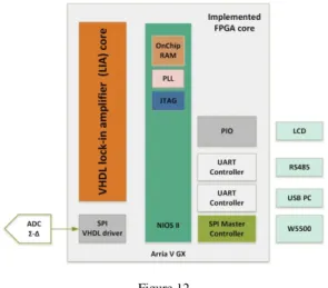
A complete overview of the designed FPGA core is in Fig. 12. The parallel tasks connected with ADC readout together with mathematical computations are implemented in the VHDL. While the data representation and communication interface is implemented inside NIOS II processor.
Figure 12 Block diagram of FPGA core
A block diagram of a LIA VHDL implementation suitable for the FPGA board is shown in Fig. 13. An ADS1263 VHDL driver serves an interface between ADC and FPGA circuit. The driver provides continuous a reading of the samples, and it also determines the sampling frequency. Sampled data are continuously provided in the bus data. The sampled data are multiplied in multiplier MUL32. The second input of the multiplier is fed by an all digital phase-locked loop PLL. The PLL generates a sine wave and a cosine wave digital waveform with a phase shift respected to the REF signal. The filtration of the frequency ωS + ωR is provided by a PERAVG and an MOVAVG filter. The PERAVG is designed as an average of one period of the input signal, and MOVAVG is designed as a moving average
filter. The filtered signal is led into a NIOS processor block that provides a necessary computation logic.
Figure 13
The VHDL implementation of the LIA
6 HW Platform Verification
A few experiments were made to verify the designed platform. For both methods (FDS and FRA) the key result depends on the precise measurement of amplitude and phase of two input signals with reference to excitation signal. Therefore, the most important part of the whole FDS and FRA analyser consists in quality of LIA implementation. The first experiment, was focused on the long-term stability of used ADC, the second experiment was focused on the sensitivity of a phase shift measurement, and the third experiment was focused on the accuracy of the phase shift measurement. The block diagram of the first and the second experiment is shown in Fig. 14.
Figure 14
The block diagram of the stability and phase sensitivity experiment
In Fig. 15 is plotted data measured by the LIA algorithm (described in Chapter 5) with a stable sinus waveform, with a frequency of 50 Hz led into the input of the front-end board. During the two hours test, no drift was observed. The root mean square error was evaluated as 1.5 µVRMS.
Figure 15
The results of the phase sensitivity experiment
The second experiment was designed to prove the phase shift sensitivity close to 0.001˚ that leads to the tangent delta of 1.75•10-5. The tested signal was generated using an arbitrary waveform generator Agilent 33522A. A minimal phase shift that can be generated using this generator in the arbitrary mode at the frequency of 50 Hz is of 0.00108˚. The sensitivity of the phase shift change of 0.00108˚ is visible from the measured data shown in Fig. 16. It is evident that the designed measuring system is able to detect at least the phase shift changes of 0.00108˚.
Figure 16
The results of the phase sensitivity experiment
The third experiment’s goal to prove the accuracy of the measurement of the phase shift. A block diagram of the experiment is shown in Fig. 17. The front-end was excited by sin waveform with the frequency of 50 Hz, and internal phase
shifter was set at different angles. Measured results are stated in Table 1, where UIN is an RMS value of input voltage, φ is a phase shift set into the internal PLL phase shifter, θ is phase computed from output values of the implemented LIA algorithm and ε is an absolute error with respect to the set internal phase shift.
Figure 17
The measurement of phase shift accuracy
Table 1
The results of the angle measurement accuracy
UIN[V] φ [rad] θ [rad] ε [rad]
0.17966 0 Π -2.55 • 10-5 2.55 • 10-5
0.17966 1/8 Π 0.39267 2.91 • 10-5
0.17966 1/4 Π 0.78537 2.82 • 10-5
0.17966 3/8 Π 1.17807 2.72 • 10-5
0.17966 1/2 Π 1.57077 2.63 • 10-5
0.35934 0 Π 1.6 • 10-5 1.6 • 10-5
0.35934 1/8 Π 0.39272 2.09 • 10-5
0.35934 1/4 Π 0.78540 1.84 • 10-5
0.35934 3/8 Π 1.17811 1.28 • 10-5
0.35934 1/2 Π 1.57078 1.63 • 10-5
Conclusions
This paper describes a design of an HW platform intended for the frequency response analysis and the frequency domain spectroscopy applied for HV machines diagnostics. Briefly mentioned is the principle of the used diagnostic methods and the requirements for an instrument implementing both methods are pointed out. The motherboard provides necessary computation to implement an algorithm of the FDS and FRA methods. To verify a functionality of the platform a basic lock-in amplifier implementation was designed. It was observed that the daughter board provides time stable results and the instrument is able to use the measurement of the dissipation factor with a resolution of 1.75•10-5 at the frequency of 50 Hz necessary for the FDS method. It was also proved an accuracy of 3•10-5 rad in measured angle, although without any sophisticated calibration.
To complete the FDS analyzer it is necessary to solve the output high-voltage amplifier (see Chapter 2). The next work will be oriented toward the testing of a commercially available amplifier. After verification of the amplifier in a practical
FDS measurement, the integration of the amplifier into FDS analyzer will be considered. Also, a calibration method of the analyzer is supposed to be developed.
Acknowledgement
This work was supported by the Grant Agency of the Czech Technical University in Prague, grant No. SGS15/213/OHK3/3T/13.
References
[1] J. S. Simons, “Diagnostic testing of high-voltage machine insulation. a review of ten years’ experience in the field,” IEE Proceedings B - Electric Power Applications, Vol. 127, No. 3, pp. 139-154, May 1980
[2] G. K. Supramaniam, Z. F. Hussien, and M. A. T, “Application of frequency domain spectroscopy (fds) in assessing dryness and ageing state of transformer insulation systems,” in Power and Energy Conference, 2008.
PECon 2008. IEEE 2nd International, Dec 2008, pp. 55-61
[3] J. P. van Bolhuis, E. Gulski, and J. J. Smit, “Monitoring and diagnostic of transformer solid insulation,” IEEE Transactions on Power Delivery, Vol.
17, No. 2, pp. 528-536, Apr 2002
[4] T. K. Saha, M. Darveniza, D. J. T. Hill, and T. T. Le, “Electrical and chemical diagnostics of transformers insulation. b. accelerated aged insulation samples,” IEEE Transactions on Power Delivery, Vol. 12, No. 4, pp. 1555-1561, Oct 1997
[5] M. S. Naidu, V. Kamaraju, and M. S. Naidu, High Voltage Engineering.
McGraw-Hill Professional Publishing, 1995
[6] M. Farahani, E. Gockenbach, H. Borsi, and M. Kaufhold, “A method for the evaluation of insulation systems for high voltage rotating machines,” in Properties and Applications of Dielectric Materials, 2003. Proceedings of the 7th International Conference on, Vol. 3, June 2003, pp. 1108-1111 [7] R. Schwarz and M. Muhr, “Diagnostic methods for transformers,” in
Condition Monitoring and Diagnosis, 2008. CMD 2008. International Conference on, April 2008, pp. 974-977
[8] B. H. Ward, “A survey of new techniques in insulation monitoring of power transformers,” IEEE Electrical Insulation Magazine, Vol. 17, No. 3, pp. 16-23, May 2001
[9] M. Farahani, H. Borsi, and E. Gockenbach, “Dielectric spectroscopy in time and frequency domain on insulation system of high voltage rotating machines,” in Solid Dielectrics, 2004. ICSD 2004. Proceedings of the 2004 IEEE International Conference on, Vol. 1, July 2004, pp. 60-63
[10] J. Britton. (2004) Transformer maintenance and diagnostics using frequency response analysis. [Online]. Available:
http://www.electricenergyonline.com
[11] J. Abhishek and P. Aaradhi, “Dielectric diagnosis of ehv current transformer using frequency domain spectroscopy (fds) & polarization and depolarization current (pdc),” International Journal of Scientific &
Engineering Research, Nov 2012
[12] OMICRON. (2016) Dielectric response analysis and moisture in oil-paper
dielectric. [Online]. Available:
https://www.omicronenergy.com/fileadmin/user upload/pdf/literature/DIRANA-Brochure-ENU.pdf
[13] A. Abu-siada, N. Hashemnia, S. Islam, and M. S. A. Masoum, “Impact of transformer model parameters variation on fra signature,” in Universities Power Engineering Conference (AUPEC), 2012 22nd Australasian, Sept 2012, pp. 1-5
[14] Z. Wang, J. Li, and D. M. Sofian, “Interpretation of transformer FRA responses 2014; part i: Influence of winding structure,” IEEE Transactions on Power Delivery, Vol. 24, No. 2, pp. 703-710, April 2009
[15] U. Sharma, S. Chatterjee, and K. Bhuyan, “Development of reference SFRA plot of transformer at design stage using high frequency modelling,”
in Power and Energy in NERIST (ICPEN), 2012 1st International Conference on, Dec 2012, pp. 1-4
[16] S. S. Patil and S. E. Chaudhari, “An attempt to investigate the transformer failure by using DGA and SFRA analysis,” in Properties and Applications of Dielectric Materials (ICPADM), 2012 IEEE 10th International Conference on the, July 2012, pp. 1-4
[17] P. T. M. Vaessen and E. Hanique, “A new frequency response analysis method for power transformers,” IEEE Transactions on Power Delivery, Vol. 7, No. 1, pp. 384-391, Jan 1992
[18] L. Coffeen, J. Britton, and J. Rickmann, “A new technique to detect winding displacements in power transformers using frequency response analysis,” in Power Tech Conference Proceedings, 2003 IEEE Bologna, Vol. 2, June 2003, p. 7